Achieving ultra-high power factor in Sb2Te2Se via valence band convergence
Abstract
An efficient approach to improve the thermoelectric performance of materials is to converge their electronic bands, which is known as band engineering. In this regard, lots of effort have been made to further improve the thermoelectric efficiency of bulk and exfoliated monolayers of Bi2Te3 and Sb2Te3. However, ultra-high band degeneracy and thus significant improvement of power factor have not been yet realized in these materials. Using first-principles methods, we demonstrate that the valley degeneracy of Bi2Te3 and Sb2Te3 can be largely improved upon substitution of the middle layer Te atoms with the more electronegative S or Se atoms. Our detailed analysis reveals that in this family of materials two out of four possible valence band valleys merely depend on the electronegativity of the middle layer chalcogen atoms, which makes the independent modulation of the valleys’ position feasible. As such, band alignment of Bi2Te3 and Sb2Te3 largely improves upon substitution of the middle layer Te atoms with more electronegative, yet chemically similar, S and Se ones. A superior valence band alignment is attained in Sb2Te2Se monolayers where the three out of four possible valleys are well-aligned, resulting in a giant band degeneracy of 18 that holds the record among all thermoelectric materials.
pacs:
xxxxxIntroduction
The electro-thermal energy conversion is an environmentally friendly solution to the global energy crisis, yet the efficiency of energy conversion should be significantly improved for practical applications of thermoelectric (TE) devices Goldsmid (2010). The efficiency of TE materials is determined by the thermoelectric figure of merit , where is the electrical conductivity, is the Seebeck coefficient or thermopower, is the absolute temperature, and are electronic and lattice contributions to the thermal conductivity, respectively. Achieving an optimal value is highly nontrivial, which requires dealing with conflicting parameters, since and are inversely related, and is proportional to as implied by the Wiedemann-Franz law ().
To improve TE performance, various strategies have been proposed, which can be majorly categorized into either i) Phonon engineering Tang et al. (2010); Majumdar (2004); Poudel et al. (2008); Dresselhaus et al. (1999) or ii) Band engineering Liu et al. (2012); Tang et al. (2015); Zhang et al. (2012); Witkoske et al. (2017); Pei et al. (2011, 2012); He et al. (2017, 2019). Thanks to the relatively decoupled nature of lattice thermal transport from the electronic properties, phonon engineering has been frequently utilized to suppress through creating nanostructures, resulting in a direct boost in . On the other hand, band engineering can be typically realized via converging separate energy pockets near the Fermi level (valley degeneracy), thus enhancing the power factor (), which is defined as . It should be noted that, increasing only, for example, through increasing the electron effective mass (), may not ultimately lead to enhancement, because it is also detrimental to . Therefore, a better scenario is a combination of multiple conducting channels composed of degenerate valleys where every single valley provides a low and thus high electron mobility Goldsmid (2013); Pei et al. (2011). Since the overall density-of-states effective mass is proportional to the orbital degeneracy, =, increasing the number of degenerate valleys simultaneously enhances the Seebeck coefficient, another advantage to attain high .
Accordingly, TE materials with intrinsically high and low have long been under intensive study, such as PbTe, Bi2Te3, Sb2Te3, Zintl to name a few. Particularly, Bismuth Telluride and its alloys have attracted considerable amount of attention Wright (1958); Goldsmid (2013); Kim et al. (2017); Yan et al. (2010) as a practical realization of TE devices. Their excellent TE performance stems from (i) the six-fold degeneracy of the valence-band maximum in the bulk Bi2Te3 Shi et al. (2015) and (ii) the intrinsically low lattice thermal conductivity of about 1.5 Goldsmid (1956), resulting in an excellent 1 at T Tritt and Subramanian (2006). In addition, it has been demonstrated by Dresselhaus et. al. Dresselhaus et al. (1999) that the emergence of quantum confinement effect by reducing the dimensionality could further improve . This strategy has been successfully applied to Bi2Te3 nanowires, where a 13% enhancement in has been achieved compared to the -type Bi2Te2.7Se0.3 bulk counterpart Zhang et al. (2011). Theoretically, exfoliated monolayers of Bi2Te3 has been predicted to attain an ultrahigh of 2.7 at Sharma and Schwingenschlögl (2016).
The present work aims to improve TE efficiency of Bi2Te3 and Sb2Te3 monolayers, and to suggest design strategies for high-performance TE materials. We show that substitution of the middle layer Te atoms with S and Se improves the valence band alignment in both Bi2Te2S and Bi2Te2Se monolayers. Particularly we attain an outstanding valence band alignment with of 18 in Sb2Te3Se monolayers, which is one of the highest reported values to the best of our knowledge. Meanwhile, all the studied materials largely benefit from their intrinsically low due to the strong anharmonicity and heavy average atomic masses Slack (1973); Lindsay et al. (2013); Naghavi et al. (2018); Peng et al. (2016a). Both of these two factors lead to a significant improvement in . Therefore, we suggest that solid solutions of Sb2Te3-xSex, Bi2Te3-xSx and Bi2Te3-xSex with =1, are more advantageous than their parent compounds for TE applications. It is also worth noting that all the studied compounds in the present work are thermodynamically stable in their bulk phase Ceder and Persson (2010); Ong et al. (2008); Jain et al. (2011) and have been predicted to be exfoliable with dynamically stable monolayers Mounet et al. (2018). The bulk Sb2Te2Se, Bi2Te2S and Bi2Te2Se have been experimentally synthesized Kanagaraj et al. (2019).
Computational Methods
In this study, we performed theoretical calculations using the Density Functional Theory (DFT) as implemented in the Vienna ab-initio Simulation Package (VASP) Kresse and Hafner (1993); Kresse and Furthmüller (1996). The projector augmented wave (PAW) pseudo-potentials Blöchl (1994); Kresse and Joubert (1999), plane wave basis set, and Perdew-Burke-Ernzerhof (PBE) exchange-correlation functionals were used Perdew et al. (1996) throughout the calculations. The cut-off energy was set to 500 eV and a -mesh sampling was used to ensure tight energy convergence. All structures were fully relaxed with respect to lattices and positions until the forces on each atom become less than 0.1 meVÅ-1. Due to the importance of Spin Orbit Coupling (SOC), we also considered this correction when calculating the electronic structure. Electronic transport properties, namely , and , were calculated by solving the Boltzmann Transport Equation (BTE) within the constant relaxation time approximation as implemented in BoltzTraP Madsen and Singh (2006). Therein, the Brillouin zone (BZ) was sampled using a dense -grid of 48481 to ensure accurate interpolation of the Kohn-Sham eigenvalues for BoltzTraP. To obtain the second order Inter-atomic Force Constants (IFCs), we used the finite displacement method as implemented in Phonopy Togo et al. (2008) code using a supercell with a -mesh of . Third order IFCs were calculated by the ShengBTE code Li et al. (2014) using supercells, with the corresponding interaction cut-off being set to the third nearest neighboring shell and -mesh sampling of the Brillouin zone.
Results and Discussion
Crystal Structure.
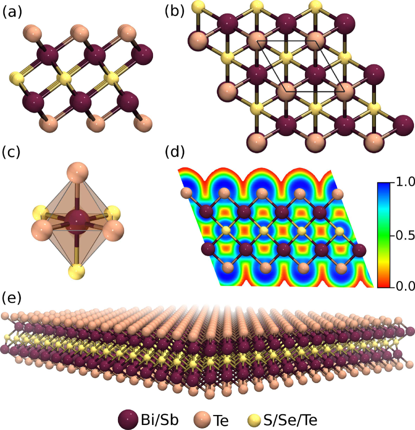
Sb2Te3 and Bi2Te3 have the space group with a rhombohedral crystal structure that belongs to the hexagonal crystal family. The bulk structure consists of quintuple layers, held together by the weak van der Waals (vdW) interaction Luo et al. (2012); Björkman et al. (2012). According to existing experiments Mounet et al. (2018); Ambrosi and Pumera (2018), monolayers of Bi2Te3 and Sb2Te3 can be exfoliated from their bulk phase at an energetic cost of 25 meV/Å2, which is comparable to the cost of peeling off a single layer of graphene from graphite. Therefore both compounds can be categorized as experimentally exfoliable materials Mounet et al. (2018).
A closer look over the crystal structure of Bi2Te3 (likewise Sb2Te3) reveals that there are two unique kinds of Te atoms in each monolayer, and thus can be labeled as Bi2[Te(1)]2[Te(2)]. In the Bi2Te3 monolayers, the number of valance electrons responsible for bonding reaches twenty-four per unit-cell, with four from each of the outer layer Te atoms (referred to as Te(1) hereafter), five from each of the Bi atoms and six from the middle layer Te atoms (Te(2)). Whereas Bi-Te(1) bond is fairly ionic in its nature, Bi-Te(2) bond is more covalent and weaker Greenaway and Harbeke (1965). It is thus expected that when one substitutes Te with a more electronegative Se or S atoms, the more weakly bound Te(2) site is energetically preferred, as shown in Fig.1. To get a deeper insight into the electronic structure of the studied monolayers, we use the electron localization function (ELF)Becke and Edgecombe (1990), which is known to be a potent tool to identify the localization of electrons and the relative orientation of lone electron pairs. The calculated ELF in Figure 1(d) reveals the mushroom shape around the outer layer Te(1) atoms, which evidence the presence of a stereochemically active anionic lone pair with its relative orientation. Our finding is consistent with the previous studies on Bi2Te3 Walsh et al. (2011); Witting et al. (2019); Lee and Elliott (2017) which shows that the anionic lone pair Walsh et al. (2011); Da Silva et al. (2008) with the -state character Lee and Elliott (2017) forms on Te(1) atoms, while lone pair Bi- states are stereochemically inactive Walsh et al. (2011); Witting et al. (2019).
Phonon Transport Properties. Principles to find materials with intrinsically low lattice thermal conductivity, which was originally proposed by Slack Slack (1973); Lindsay et al. (2013); Naghavi et al. (2018); Peng et al. (2016a), include, (i) having high average atomic mass, (ii) weak inter-atomic bonding, (iii) complex crystal structure, and (iv) strong anharmonicity, measured by Grüneisen parameter.
In many materials including monolayers, a high average mass () leads to a relatively low Debye temperature () and consequently low acoustic phonon velocities Lindsay et al. (2013). According to this insight, a lower lattice thermal conductivity in Bi2Te3 is expected compared to that of Sb2Te3, majorly because of the heavier atomic mass of Bi compared to Sb. On the other hand, the bond strength also plays an important role in determining the lattice thermal conductivity, e.g., for monolayers of Mo and W dichalcogenides Huang and Zeng (2015); Peng et al. (2016a), wherein increasing (decreasing) cation (anion) nucleon number leads to stronger (weaker) bonding and higher (lower) thermal conductivity. In this regard, the projected Crystal Orbital Overlap Population (pCOOP) and projected Crystal Orbital Hamilton Population (pCOHP) are potent tools for analyzing chemical bonds in solid Deringer et al. (2011); Dronskowski and Bloechl (1993); Hoffmann (1987). The calculated pCOOP and pCOHP are shown in Fig. S8 of SI. The integrated values with respect to energy up to for both IpCOOP and IpCOHP can be used to analyze the bond strength Maintz et al. (2016, 2013): the more overlap the orbitals have, the stronger the associated bonds are. The calculated value for Sb–Te bond in Sb2Te2Se is about 14% higher than that of Bi–Te bond in Bi2Te2Se monolayers. Therefore according to Slack’s theory Slack (1973), the lower thermal conductivity of Bi2Te2Se monolayers may be partially due to both weaker interatomic bonds and the heavier atomic mass of Bi compared to Sb.
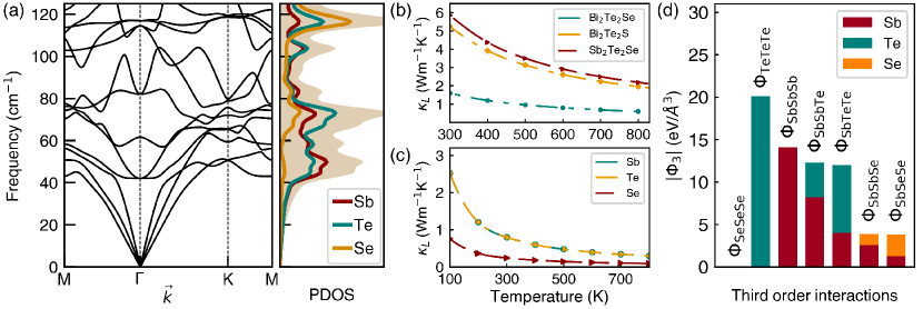
Figure 2(a) shows that Sb2Te2Se monolayer is dynamically stable with no imaginary modes through the whole BZ. The corresponding atom-decomposed phonon density of states (DOS) shows that in frequencies ranging from 0 to just below 60 cm-1—the range which contributes the most to lattice heat transport—the contribution of Sb and Te atoms to DOS are similar. The quantitative description of for the studied monolayers is shown in Figure 2(b). The of Sb2Te2Se is 6 Wm-1K-1 at 300 K, much lower than the well-studied TE monolayers such as MoS2 and WSe2, with the of 140 and 42 Wm-1K-1, respectively Kumar and Schwingenschlogl (2015). The calculated atom-decomposed lattice thermal conductivity shows that Sb and Te atoms are equally contributing to (see Figure 2(c)), consistent with our earlier analysis of the DOS. Moreover, branch decomposed thermal conductivity (Fig. S5, SI) demonstrates that the optical branches contribute poorly to , hardly reaching 18% at high temperatures. The largest contributions belong respectively to transverse acoustic (TA), longitudinal acoustic (LA), and out-of-plane acoustic (ZA) branches. The analysis of the mean free path cumulative lattice thermal conductivity (Fig. S7, SI) reveals that the can be further suppressed by decreasing the grain size of the polycrystals; for example, at the size of 100 nm the reduces by 50%.
Grüneisen parameter () measures the anharmonicity of crystalline systems and based on Slack’s theory Slack (1973) it is inversely ( related to the lattice thermal conductivity, . The larger the the stronger the anharmonicity and thus the lower the . The Grüneisen parameters of Sb2Te2Se and MoS2 are shown in Fig. S6(d) and for the transition metal dichalcogenides (TMDs) are reported in Ref.Peng et al. (2016b). The calculated Grüneisen parameters of acoustic and low-lying optical modes of Sb2Te2Se (i.e.,, heat-carrying phonons) evidence not only much higher mode values than MoS2 and other TMDs but also stronger -dependence, rendering an intrinsic and large anharmonicity in Sb2Te2Se. As expected, the of Sb2Te2Se at 300 K ( 6 Wm-1K-1) is more than 7 times lower than that of WSe2 ( 42 Wm-1K-1 Gandi and Schwingenschlögl (2016)) while the atomic mass of W (183.84 amu) is larger than Sb (121.76 amu) and Te (127.6 amu). As discussed in the following paragraph, the origin of anharmonicity in Sb2Te3 is traced back to anionic lone pair of Te atoms.
To find out the fundamental origin of the anharmonicity in Sb2Te2Se, we calculate the norm of the third-order interatomic force constants (IFCs), which is defined as = ( and are the total energy and atom displacement for different atom species , , and ). Since (i) a large absolute value of suggests strong anharmonicity and (i) the phonon scattering rates are roughly proportional to , it can be seen in Figure 2(d) that the strongest anharmonicity is associated with the , namely, the outer layer Te atoms where the lone pair electrons are stereochemically active. Consistent with previous studies Dutta et al. (2019); Nielsen et al. (2013), the presence of lone pair electrons, localized on Te atoms, could enforce anharmonicity and subsequently lower the lattice thermal conductivity of a crystal.
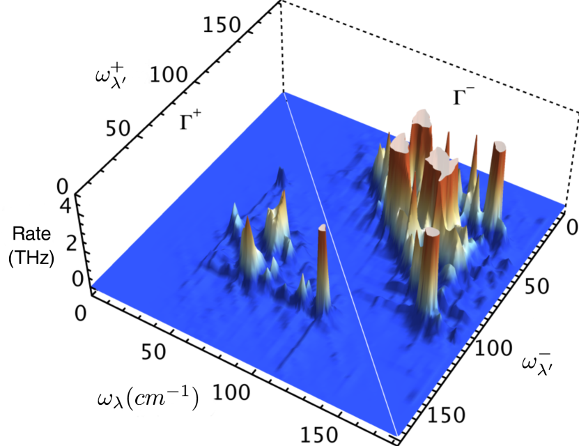
To further shed light on how phonons are scattered in Sb2Te2Se, we show in Figure 3 the frequency-dependent scattering rates arising from the three-phonon interactions, namely, the absorption (: + ) and emission (: + ) processes. The peaks in the scattering rates plot depict the scattering magnitude of the first phonon mode () induced by the second phonon mode (), satisfying both energy and crystal momentum conservation. It can be seen that the low-frequency phonon modes ( 50 cm-1) are only weakly scattered, which majorly originates from the absorption process, consistent with their long lifetimes as shown in Fig.S6(c). In contrast, the optical phonon modes are strongly scattered during various emission processes, resulting in small contributions to lattice heat conduction.
Electron Transport Properties. Considering the similarity in the electronic structure of the studied materials, we take Sb2Te2Se as an example here. As shown in Figure 4, Sb2Te2Se is a semiconductor with an indirect band-gap of 0.44 eV (including spin orbit coupling). Figure 4(c) (see Fig. S3, SI, for all family members) show nearly significant contributions of chalcogen and pnictide atoms in both valence and conduction bands, which is consistent with the covalent nature of bonding in this family of semiconductors Witting et al. (2019); Lee and Elliott (2017); Deringer et al. (2015). Note that the per atom contributions from Se and Te in the calculated total DOS are similar, however, there are two times more Te atoms than Se in the unit cell, and thus a larger contribution from Te atoms in the valence band is expected.
What turns this family into outstanding and the most studied TE materials Hung et al. (2019); Sharma and Schwingenschlögl (2016); Lee et al. (2018); Zhou and Wang (2015); Xu et al. (2018), beside low lattice thermal conductivity, is their excellent electronic transport properties and relatively high compared to other single layer TE candidates. The feature in the band structure of these monolayers that enhances their is the high band degeneracy , which is usually observed when several valleys with the same energies occur near the Fermi level or when the valley is located at a low symmetry point of the Brillouin zone of a high symmetry lattice (valley degeneracy). For the symmetry, valley degeneracy between both and is 6 and thus the is just six times the number of energetically degenerate valence band maximum (VBM) at different points in the Brillouin zone. The degeneracy that could occur among VBMs is indeed numerical, also called accidental Garrity (2016) or band convergence Tang et al. (2015). Therefore, the energy differences between four potential extrema (see Fig. 4(c) for VB1,VB2,VB3,VB4) with respect to VBM is listed in Table S1, SI. As discussed in previous studies T. Hung et al. (2019); Hung et al. (2019), has an exponential dependent on , , reaching its maximum value at . As seen in Table S1 the energy difference () between VBM (here VB1) and the next highest VB (here VB4) of Bi2Te3 and Sb2Te3 are 16 and 42 meV respectively, leaving one VBM at Fermi level, and leading to . Although the other three valleys are just slightly lower in energy, larger than 12 is not reachable by strain engineering. That is because when strain is induced, different valleys in the band structure counteract and raising one results in lowering the others, making further tuning of the valence band insurmountable. For instance, defining as a measure of change in lattice constant, our calculations for the case of Bi2Te3 demonstrated that only 4% strain doubled from 6 to 12 and increased the by one-tenth (see Fig. S1, SI), but this would be an upper limit to .
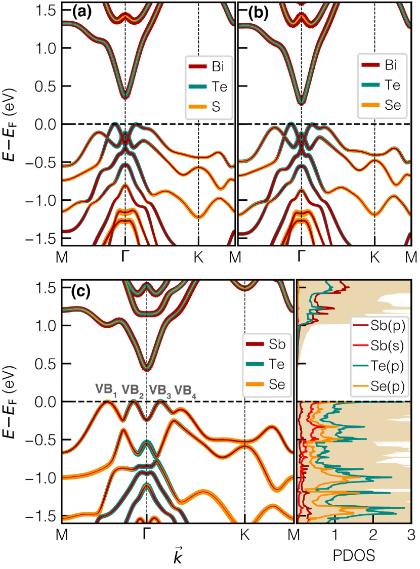
Substitution of Te(2) atoms with S and Se adequately improves band convergence of Bi2Te3 and Sb2Te3 monolayers by lowering the to meV which can be considered as almost degenerate extrema approaching . The giant band degeneracy of 18 occurs in Sb2Te2Se monolayers in which the two band extrema in – direction and the one in – direction are well-aligned (with numerical differences meV). To further understand how atom substitution leads to band alignment, we resort to atom resolved band structure calculations.
The atom decomposed band structure reveals that beside Sb/Bi atoms, the outer layer chalcogen atoms (mainly their -state as shown in DOS of Figure 4(c)) are significantly contributing to VB2 and VB3: that is to say, these extrema mainly inherit the character of the Te(1) atoms (bold green line). On the contrary, in the VB1 and VB4, the middle layer chalcogen atoms (i.e., Te(2) have the dominant contribution (bold orange line). Therefore, one can independently tune the height of VB1,4 with respect to VB2,3 by changing the middle layer atoms. As seen in Fig.S2, SI, substitution of the middle layer Te(2) atoms with the more electronegative Se ones in Sb2Te3 lowers the height of VB1,4 with respect to the VB2,3 , which leads to the alignment of VB1,2,3, and to in Sb2Te2Se as highlighted in Figure 4(c). The same observation holds for S substituted monolayers, however, due to higher electronegativity of S compared to Se the VB1 and VB4 extrema decrease a lot that leave only the two central extrema aligned, leading to in Sb2Te2S.
Using a Constant Relaxation Time Approximation (CRTA), we calculated electronic transport coefficients for Bi2Te2S, Bi2Te2Se and Sb2Te2Se monolayers at varying temperatures by solving the Boltzmann transport equation. To estimate electronic transport properties of materials the choice of electron relaxation time is critical. From comparison with experimental data at 300 K, N. F. Hinsche et al. Hinsche et al. (2011) determined the in-plane = s and s for the Sb2Te3 and Bi2Te3, respectively. Also, fitted values such as s Scheidemantel et al. (2003); Zhou and Wang (2015) and Lee et al. (2018) were suggested for Bi2Te3 at 300 K. Likewise, for Bi2Te2S the in-plane relaxation time of s was used Joo et al. (2019). N. T. Hung et al., Hung et al. (2019) calculated the relaxation time in Bi2{S, Se, Te}3 monolayers and found it to be s, much lower than their 3D counterparts. They claimed that shorter for 2D materials is due to quantum confinement effect Hicks and Dresselhaus (1993) which increases the density of electronic states in 2D systems. Here we use s and s, as suggested by Ref. Hinsche et al. (2011) and Ref. Hung et al. (2019) to estimate the of the studied materials. However, because of possible uncertainties in the estimation of and to make the comparison to previous work easier, we also report the and for different (color bar) within a range from 0.2 to 4.4 s in Fig. S9 of SI, covering all the previously reported .
Assuming s, the calculated of Sb2Te2Se at three different temperatures are compared to other studied compounds. Note that the increase in at higher temperatures is due to a constant relaxation time adopted in all three temperatures, while in reality the relaxation time decreases with increasing temperature (roughly by for Bi2Te3 Zhou and Wang (2015)). As seen in Figure 5(a), using s at K our calculated for Bi2Te3 is about 4 that agrees well with the reported in the previous study Zhou and Wang (2015). This increases to 7 by substitution of Te with Se atom as in Bi2Te2Se. Likewise, the of Sb2Te3 increases by a factor of two upon Se substitution, achieving a giant in Sb2Te2Se at 300 K as seen in Figure 5(b). Using the same and temperature, the maximum for MoS2, MoSe2, TiS3, Pd2Se3 are respectively 1.8 Babaei et al. (2014) (n-type), 0.8 Kumar and Schwingenschlogl (2015) (n-type) and 1.8 Zhang et al. (2017) (n-type) and 1.6 Naghavi et al. (2018) (p-type). Due to the much larger and much smaller compared to these materials (e.g., of Sb2Te2Se at 300 K is 6 Wm-1K-1 and MoS2 131 Wm-1K-1 Gandi and Schwingenschlögl (2016)) we expect a high figure of merit in Sb2Te2Se, thus enabling high thermoelectric efficiency.
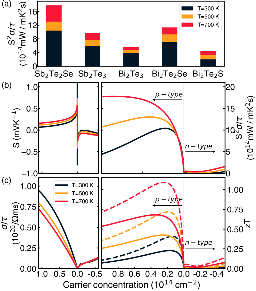
Thermoelectric Figure of Merit. Figure 5(c) shows the calculated for the Sb2Te2Se at three different relaxation times and temperatures. Even assuming as small as s we could reach the of 0.7 and 0.22 at 700 and 300 K, respectively. Considering the same relaxation time, the calculated values are much larger than other proposed monolayers such as WSe2 Kumar and Schwingenschlogl (2015) and TiS3 Zhang et al. (2017) and SnSe Wang et al. (2015). For example, using the same the calculated at 700 K for Sb2Te2Se is 30% larger than SnSe monolayers Wang et al. (2015), which has the highest record in the bulk phase Zhao et al. (2014).
It is worth nothing that the estimated in this work could be considered as a lower limit, because the used electron relaxation time is quite small and the calculated tends to be larger than the experimental one. For example, the calculated for MoS2 monolayers is 131 Wm-1K-1 Gandi and Schwingenschlögl (2016) while experimental value of 34.5 Wm-1K-1 was measured Yan et al. (2014), which could be due to point defects, dislocations, and finite size effect. Therefore, the real could be larger than our estimation.
Conclusions
We investigated electronic structure, phonon and electron transport properties of Te (M=Bi, Sb; X=S, Se, Te) monolayers by the means of first-principles calculations and Boltzmann transport theory. Our detailed analysis reveal that four reachable valence band extrema exist in this family of materials and that two of them merely depends on the electronegativity of the middle layer chalcogen atoms, which makes the independent modulation of the vallyes’ position doable. As such we substitute the middle layer Te with isoelectronic equivalents S, and Se atoms and found that the band alignment significantly improves transport properties of both Bi2Te3 and Sb2Te3. The superior valence band alignment occurs in Sb2Te2Se monolayers where the trhee out of four possible valleys are well-aligned resulting in the giant band degeneracy of 18 that the hold a record among all thermoelectric materials. Our results demonstrate that in this family of monolayers, is comparable to, and can be better than many well-known thermoelectric compounds. It should also be noted that the reported values for in these materials are only lower limits, since nanostructuring can significantly deteriorate lattice thermal conductivity by almost 50 percent. Our finding could advance the thermoelectric materials design, where the convergence of electronic band is achieved by tuning the composition.
References
- Goldsmid (2010) H. J. Goldsmid, Introduction to thermoelectricity, Vol. 121 (Springer, 2010).
- Tang et al. (2010) J. Tang, H.-T. Wang, D. H. Lee, M. Fardy, Z. Huo, T. P. Russell, and P. Yang, Nano letters 10, 4279 (2010).
- Majumdar (2004) A. Majumdar, Science 303, 777 (2004).
- Poudel et al. (2008) B. Poudel, Q. Hao, Y. Ma, Y. Lan, A. Minnich, B. Yu, X. Yan, D. Wang, A. Muto, D. Vashaee, et al., Science 320, 634 (2008).
- Dresselhaus et al. (1999) M. Dresselhaus, G. Dresselhaus, X. Sun, Z. Zhang, S. Cronin, and T. Koga, Physics of the Solid State 41, 679 (1999).
- Liu et al. (2012) W. Liu, X. Tan, K. Yin, H. Liu, X. Tang, J. Shi, Q. Zhang, and C. Uher, Physical Review Letters 108, 166601 (2012).
- Tang et al. (2015) Y. Tang, Z. M. Gibbs, L. A. Agapito, G. Li, H.-S. Kim, M. B. Nardelli, S. Curtarolo, and G. J. Snyder, Nature materials 14, 1223 (2015).
- Zhang et al. (2012) Q. Zhang, F. Cao, W. Liu, K. Lukas, B. Yu, S. Chen, C. Opeil, D. Broido, G. Chen, and Z. Ren, Journal of the American chemical society 134, 10031 (2012).
- Witkoske et al. (2017) E. Witkoske, X. Wang, M. Lundstrom, V. Askarpour, and J. Maassen, Journal of Applied Physics 122, 175102 (2017).
- Pei et al. (2011) Y. Pei, X. Shi, A. LaLonde, H. Wang, L. Chen, and G. J. Snyder, Nature 473, 66 (2011).
- Pei et al. (2012) Y. Pei, H. Wang, and G. J. Snyder, Advanced materials 24, 6125 (2012).
- He et al. (2017) J. He, S. Hao, Y. Xia, S. S. Naghavi, V. Ozolins, and C. Wolverton, Chemistry of Materials 29, 2529 (2017).
- He et al. (2019) J. He, Y. Xia, S. S. Naghavi, V. Ozoliņš, and C. Wolverton, Nature communications 10, 719 (2019).
- Goldsmid (2013) H. Goldsmid, Thermoelectric refrigeration (Springer, 2013).
- Wright (1958) D. Wright, Nature 181, 834 (1958).
- Kim et al. (2017) H.-S. Kim, N. A. Heinz, Z. M. Gibbs, Y. Tang, S. D. Kang, and G. J. Snyder, Materials Today 20, 452 (2017).
- Yan et al. (2010) X. Yan, B. Poudel, Y. Ma, W. Liu, G. Joshi, H. Wang, Y. Lan, D. Wang, G. Chen, and Z. Ren, Nano letters 10, 3373 (2010).
- Shi et al. (2015) H. Shi, D. Parker, M.-H. Du, and D. J. Singh, Physical Review Applied 3, 014004 (2015).
- Goldsmid (1956) H. Goldsmid, Proceedings of the Physical Society. Section B 69, 203 (1956).
- Tritt and Subramanian (2006) T. M. Tritt and M. Subramanian, MRS bulletin 31, 188 (2006).
- Zhang et al. (2011) G. Zhang, B. Kirk, L. A. Jauregui, H. Yang, X. Xu, Y. P. Chen, and Y. Wu, Nano letters 12, 56 (2011).
- Sharma and Schwingenschlögl (2016) S. Sharma and U. Schwingenschlögl, ACS Energy Lett. 1, 875 (2016).
- Slack (1973) G. A. Slack, Journal of Physics and Chemistry of Solids 34, 321 (1973).
- Lindsay et al. (2013) L. Lindsay, D. Broido, and T. Reinecke, Physical review letters 111, 025901 (2013).
- Naghavi et al. (2018) S. S. Naghavi, J. He, Y. Xia, and C. Wolverton, Chemistry of Materials 30, 5639 (2018).
- Peng et al. (2016a) B. Peng, H. Zhang, H. Shao, Y. Xu, R. Zhang, H. Lu, D. W. Zhang, and H. Zhu, ACS applied materials & interfaces 8, 20977 (2016a).
- Ceder and Persson (2010) G. Ceder and K. Persson, “The materials project: A materials genome approach,” (2010).
- Ong et al. (2008) S. P. Ong, L. Wang, B. Kang, and G. Ceder, Chemistry of Materials 20, 1798 (2008).
- Jain et al. (2011) A. Jain, G. Hautier, S. P. Ong, C. J. Moore, C. C. Fischer, K. A. Persson, and G. Ceder, Physical Review B 84, 045115 (2011).
- Mounet et al. (2018) N. Mounet, M. Gibertini, P. Schwaller, D. Campi, A. Merkys, A. Marrazzo, T. Sohier, I. E. Castelli, A. Cepellotti, G. Pizzi, et al., Nature nanotechnology 13, 246 (2018).
- Kanagaraj et al. (2019) M. Kanagaraj, A. Pawbake, S. C. Sarma, V. Rajaji, C. Narayana, M.-A. Measson, and S. C. Peter, Journal of Alloys and Compounds 794, 195 (2019).
- Kresse and Hafner (1993) G. Kresse and J. Hafner, Physical Review B 48, 13115 (1993).
- Kresse and Furthmüller (1996) G. Kresse and J. Furthmüller, Computational materials science 6, 15 (1996).
- Blöchl (1994) P. E. Blöchl, Physical review B 50, 17953 (1994).
- Kresse and Joubert (1999) G. Kresse and D. Joubert, Physical review b 59, 1758 (1999).
- Perdew et al. (1996) J. P. Perdew, K. Burke, and M. Ernzerhof, Physical review letters 77, 3865 (1996).
- Madsen and Singh (2006) G. K. Madsen and D. J. Singh, Computer Physics Communications 175, 67 (2006).
- Togo et al. (2008) A. Togo, F. Oba, and I. Tanaka, Physical Review B 78, 134106 (2008).
- Li et al. (2014) W. Li, J. Carrete, N. A. Katcho, and N. Mingo, Computer Physics Communications 185, 1747 (2014).
- Luo et al. (2012) X. Luo, M. B. Sullivan, and S. Y. Quek, Physical Review B 86, 184111 (2012).
- Björkman et al. (2012) T. Björkman, A. Gulans, A. V. Krasheninnikov, and R. M. Nieminen, Physical review letters 108, 235502 (2012).
- Ambrosi and Pumera (2018) A. Ambrosi and M. Pumera, Chemical Society Reviews 47, 7213 (2018).
- Greenaway and Harbeke (1965) D. L. Greenaway and G. Harbeke, Journal of Physics and Chemistry of Solids 26, 1585 (1965).
- Becke and Edgecombe (1990) A. D. Becke and K. E. Edgecombe, The Journal of chemical physics 92, 5397 (1990).
- Walsh et al. (2011) A. Walsh, D. J. Payne, R. G. Egdell, and G. W. Watson, Chemical Society Reviews 40, 4455 (2011).
- Witting et al. (2019) I. T. Witting, T. C. Chasapis, F. Ricci, M. Peters, N. A. Heinz, G. Hautier, and G. J. Snyder, Advanced Electronic Materials , 1800904 (2019).
- Lee and Elliott (2017) T. H. Lee and S. R. Elliott, Advanced Materials 29, 1700814 (2017).
- Da Silva et al. (2008) J. L. Da Silva, A. Walsh, and H. Lee, Physical Review B 78, 224111 (2008).
- Huang and Zeng (2015) L.-F. Huang and Z. Zeng, The Journal of Physical Chemistry C 119, 18779 (2015).
- Deringer et al. (2011) V. L. Deringer, A. L. Tchougreeff, and R. Dronskowski, J. Phys. Chem. A 115, 5461 (2011).
- Dronskowski and Bloechl (1993) R. Dronskowski and P. E. Bloechl, J. Phys. Chem. 97, 8617 (1993).
- Hoffmann (1987) R. Hoffmann, Angew. Chem. Int. Ed. Engl. 26, 846 (1987).
- Maintz et al. (2016) S. Maintz, V. L. Deringer, A. L. Tchougréeff, and R. Dronskowski, Journal of computational chemistry 37, 1030 (2016).
- Maintz et al. (2013) S. Maintz, V. L. Deringer, A. L. Tchougréeff, and R. Dronskowski, Journal of computational chemistry 34, 2557 (2013).
- Kumar and Schwingenschlogl (2015) S. Kumar and U. Schwingenschlogl, Chemistry of Materials 27, 1278 (2015).
- Peng et al. (2016b) B. Peng, H. Zhang, H. Shao, Y. Xu, X. Zhang, and H. Zhu, RSC Adv. 6, 5767 (2016b).
- Gandi and Schwingenschlögl (2016) A. N. Gandi and U. Schwingenschlögl, EPL (Europhysics Lett. 113, 36002 (2016).
- Dutta et al. (2019) M. Dutta, K. Pal, U. V. Waghmare, and K. Biswas, Chemical science 10, 4905 (2019).
- Nielsen et al. (2013) M. D. Nielsen, V. Ozolins, and J. P. Heremans, Energy & Environmental Science 6, 570 (2013).
- Deringer et al. (2015) V. L. Deringer, R. P. Stoffel, M. Wuttig, and R. Dronskowski, Chemical Science 6, 5255 (2015).
- Hung et al. (2019) N. T. Hung, A. R. Nugraha, and R. Saito, Nano Energy 58, 743 (2019).
- Lee et al. (2018) C. Lee, J. N. Kim, J.-Y. Tak, H. K. Cho, J. H. Shim, Y. S. Lim, and M.-H. Whangbo, AIP Adv. 8, 115213 (2018).
- Zhou and Wang (2015) G. Zhou and D. Wang, Sci. Rep. 5 (2015).
- Xu et al. (2018) B. Xu, J. Zhang, G. Yu, S. Ma, Y. Wang, and Y. Wang, J. Appl. Phys. 124, 165104 (2018).
- Garrity (2016) K. F. Garrity, Physical Review B 94, 045122 (2016).
- T. Hung et al. (2019) N. T. Hung, A. R. Nugraha, T. Yang, Z. Zhang, and R. Saito, Journal of Applied Physics 125, 082502 (2019).
- Hinsche et al. (2011) N. Hinsche, B. Y. Yavorsky, I. Mertig, and P. Zahn, Physical Review B 84, 165214 (2011).
- Scheidemantel et al. (2003) T. J. Scheidemantel, C. Ambrosch-Draxl, T. Thonhauser, J. V. Badding, and J. O. Sofo, Phys. Rev. B 68, 125210 (2003).
- Joo et al. (2019) S.-J. Joo, B. Ryu, J.-H. Son, J. E. Lee, B.-K. Min, and B.-S. Kim, Journal of Alloys and Compounds 783, 448 (2019).
- Hicks and Dresselhaus (1993) L. Hicks and M. S. Dresselhaus, Physical Review B 47, 12727 (1993).
- Babaei et al. (2014) H. Babaei, J. Khodadadi, and S. Sinha, Applied Physics Letters 105, 193901 (2014).
- Zhang et al. (2017) J. Zhang, X. Liu, Y. Wen, L. Shi, R. Chen, H. Liu, and B. Shan, ACS Appl. Mater. Interfaces 9, 2509 (2017).
- Wang et al. (2015) F. Q. Wang, S. Zhang, J. Yu, and Q. Wang, Nanoscale 7, 15962 (2015).
- Zhao et al. (2014) L.-D. Zhao, S.-H. Lo, Y. Zhang, H. Sun, G. Tan, C. Uher, C. Wolverton, V. P. Dravid, and M. G. Kanatzidis, Nature 508, 373 (2014).
- Yan et al. (2014) R. Yan, J. R. Simpson, S. Bertolazzi, J. Brivio, M. Watson, X. Wu, A. Kis, T. Luo, A. R. Hight Walker, and H. G. Xing, ACS Nano 8, 986 (2014).