Theory of valley-resolved spectroscopy of a Si triple quantum dot coupled to a microwave resonator
Abstract
We theoretically study a silicon triple quantum dot (TQD) system coupled to a superconducting microwave resonator. The response signal of an injected probe signal can be used to extract information about the level structure by measuring the transmission and phase shift of the output field. This information can further be used to gain knowledge about the valley splittings and valley phases in the individual dots. Since relevant valley states are typically split by several , a finite temperature or an applied external bias voltage is required to populate energetically excited states. The theoretical methods in this paper include a capacitor model to fit experimental charging energies, an extended Hubbard model to describe the tunneling dynamics, a rate equation model to find the occupation probabilities, and an input-output model to determine the response signal of the resonator.
Semiconductors with abundant nuclear spin-free isotopes are increasingly being investigated as host material for spin qubits, e.g. silicon [1], germanium[2], and graphene [3, 4]. It turns out that most of these materials comprise an electron valley degree of freedom [5] in the conduction band of the bulk material. In many nanostructures based on these semiconductor materials, the resulting valley splitting is still not fully understood and therefore represents in practice an unpredictable system parameter. It is known that the valley degree of freedom can be described as a pseudo-spin in a two dimensional electron gas (2DEG) whose attributes, i.e., valley-splitting and valley-phase, drastically depend on the interface of the heterostructure [6, 7, 8, 9, 10, 11, 12, 13]. A single atomic step can change the quantization axis of the pseudo-spin and the complex phase of the valley-orbit coupling of an electron can be modified by as much as [11, 12, 13]. This has a large impact on silicon quantum computation [1] for most qubit implementations, which use the spin degree of freedom to encode quantum information [14]. For multi-qubit quantum processors [15, 16, 17, 18] and multi-spin qubit implementations [19, 20, 21, 22], the presence of the valley leads to several non-computational states into which the information can “leak”. Since the number of leakage states exponentially increases with the number of electrons, the resulting complex energy diagram with a high density of states makes it difficult to find the optimal parameter regimes for encoding and operating such qubits. Therefore, a precise knowledge of the valley structure is required for high-fidelity qubit implementations and operations. A lower bound to the valley splitting can be obtained using ground-state magnetospectroscopy [23, 24, 25, 26, 27]. Recent advances in the coupling of electrons to superconducting microwave resonators [28, 29, 30, 31, 32, 33, 34, 35] allow for precise read-out of the valley splittings in double quantum dots [36, 32]. In this theoretical paper, the technique is extended and adapted to extract the valley splitting and valley phases in a silicon triple quantum dot (TQD) system using such superconducting microwave resonator.
This paper is organized as follows. Firstly, we introduce a general theoretical model of the TQD system in Section 1. For this we use a classical capacitor model to find the electrostatic energies of the electrons and substitute them into an extended Hubbard model to account for hopping of the electrons between the dots (see subsection 1.1). Subsequently in subsection 1.2, we use a master equation to find the steady state solution of the electron dynamics in the presence of dissipative processes. This allows us to find the corresponding occupation probabilities. Finite temperature effects and an externally applied bias are included in our model. In subsection 1.3, we consider the response of a superconducting microwave cavity dispersively coupled to the TQD system and use input-output theory to derive analytical expressions for the response signal. Subsequently, in Section 2, we show how one can extract relevant system parameters from the cavity response signal. We explicitly demonstrate the case of a single electron in a triple quantum dot in subsection 2.1 and the case of three electrons in subsection 2.2.
1 Theoretical description
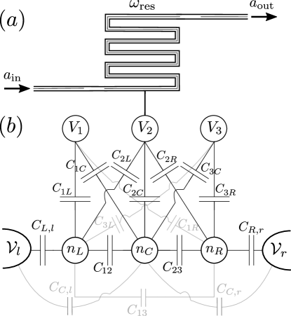
We consider a triple quantum dot (TQD) connected to two leads and a superconducting transmission line resonator via the center gate (see Fig. 1). In order to describe the TQD theoretically, we first construct the bare electron Hamiltonian of the system and introduce the interaction to the leads and the microwave resonator later. We consider a basis with 0, 1, 2 or 3 electrons with spin and two-fold valley degeneracy in each dot. For a fixed number of electrons , there are possible basis states with being the product of the number of dots , the spin degeneracy , and the valley degeneracy . Therefore, we have basis states in total. Here, we restrict our analysis to the two energetically lowest laying orbital levels. Silicon quantum dots typically have relatively large orbital energies = [37, 38], thus, the impact of higher orbital levels can be neglected for temperatures and applied voltage biases where is the electron charge and is the norm of the lever arm matrix [39].
1.1 Hamiltonian
In order to obtain a good agreement of our theoretical studies with experiments we rely on a description with the extended Hubbard model. The electrostatic energies are given by a capacitor model of the TQD, schematically shown in Fig. 1. The free energy of the triple dot system reads [40]
| (1) |
where denotes the transposition and
| (2) |
quantifies the total effective charge on the quantum dots composed of the electron occupation number and the applied gate voltages . Here denotes the electron charge and the applied bias voltages between the left and right leads. The dot capacitance matrix reads
| (6) |
which contains the self capacitances and the mutual capacitances , and . The capacitances between the gates and the dots reads
| (10) |
and
| (14) |
contains the capacitances between the dots and the left and right lead. For later convenience we also define the chemical potential in each dot
| (15) | ||||
| (16) | ||||
| (17) |
The total Hamiltonian of the hybrid TQD-resonator system is given by
| (18) |
where the individual contributions are introduced below.
The electrostatic interaction is described by the Hamiltonian
| (19) | ||||
| (20) |
with and the free energy defined in Eq. (1). Here () creates (annihilates) an electron in dot , with spin , and occupying the valley state.
An externally applied magnetic field breaks the spin-degeneracy. Considering a homogeneous magnetic field , the Zeeman splitting is described by
| (21) |
with . The Zeeman energy is where is the electron g-factor in silicon. To be precise, the electron g-factor depends on the valley and orbital level and is slightly anisotropic giving rise to small effective magnetic field gradients [41]. Here, this small anisotropy is neglected.
For a silicon heterostructure the two minima in the conduction band [1] give rise to the valley degree of freedom. The valley splitting can be expressed locally in QD as [6]
| (24) |
with the complex quantity consisting of the valley splitting and valley phase in dot . Because of atomistic defects at the silicon interface the valley pseudo-vector can have a different phase in each dot [36, 11, 42, 22]. The valley Hamiltonian in the valley eigenbasis of each dot can be written as
| (25) |
with . In this particular choice of representation the valley phase is transferred to the coupling matrix elements between the quantum dots. The single-qubit inter-dot matrix elements in the valley eigenbasis can be expressed as [36]
| (26) |
with , , and . The real-valued quantities can be visually interpreted as the angle between the direction of the valley pseudo-spin in dot and dot .
Off-diagonal elements of allow for coherent hopping of electrons between neighboring quantum dots. In our model hopping is only allowed between basis states with the same total electron number, the same total spin, and conserves the valley. Because of Eq. (26), the tunneling Hamiltonian reads as
| (27) |
with . We define
| (28) | ||||
| (29) | ||||
| (30) | ||||
| (31) | ||||
| (32) | ||||
| (33) |
The tunnel barriers are assumed to be adjusted such that the hopping matrix elements between the ground states are equal in strength, i.e., . Note that, to warrant a unique stationary solution (see below), we chose the valley phases and with integer . Because of the linear alinement of the TQD direct hopping between the left and the right dot becomes negligible, thus, we set . As a consequence the valley phase becomes undetectable.
1.2 Occupation probabilities
In order to calculate the occupation probabilities of the dots in the stationary state, we assume that incoherent transitions can occur between the eigenstates of , both internally and via electron hopping between the TQD and the leads. These incoherent interactions with the environment can be taken into account with the Lindblad master equation
| (34) |
where is the reduced Planck constant and is the density matrix. The dissipative part consists of the following terms
| (35) |
Here is the usual Lindbald super operator, is the transition rate from the lead to the dot , and the operators , and create and annihilate an electron in dot and valley with spin , respectively. The first and second terms of (35) correspond to the flow of electrons from lead into dot and in the opposite direction, out of the dot to the lead. The third term in (35) describes excitations within the TQD, i.e. incoherent interactions with a bosonic bath, such as phonons, that can induce transitions from one eigenstate of to the other with the same total number of electrons in the dots with the same total spin. The operator takes the system from an initial state to a final state with a transition rate .
We assume that the level broadenings, caused by the interaction with the leads and the bosonic bath, are smaller than the level splittings between the eigenstates of which we ensure by an external magnetic field . This is the so-called secular approximation [43], which results in a steady-state density matrix diagonal in the eigenbasis of . This significantly simplifies the Lindblad equation (34), where the commutator vanishes and after taking the matrix representation of the remaining dissipative term in the eigenbasis of , we obtain Redfield equations for the diagonal elements of the steady-state solution
| (36) |
where runs over all diagonal elements of . The terms in (36) are approximations of their respective counterparts in (35). Here is the -th diagonal element of the density matrix , and , which can be finite only if there is one more electron in state than in .
We can extend this description toward finite temperatures in the leads with the following replacement rules in Eq. (36)
| (37a) | |||||
| (37b) | |||||
where , and are the eigenenergies, and the number of electrons in the given eigenstates of , and
| (38) |
is the Fermi-Dirac distribution of the electrons in the lead , with and being the Boltzmann constant and the electron temperature.
To include finite temperature effects in Eq. (36) the transition rates in (36) are redefined as with the temperature dependent prefactor
| (39) |
which accounts for the Bose-Einstein statistics of the environmental thermal bath, that is assumed to be in thermal equilibrium with the electronic system and having an approximately constant density of states in the relevant energy window of the transitions. Moreover, denotes the Heaviside step function.
We use the following phenomenological model to describe incoherent decay from with rate
| (40) |
where denotes the eigenstate of the unperturbed system given in Eq. (18) with eigenenergy . In our model denotes the absolute-valued eigenvector obtained by taking the absolute value of each entry in in the eigenbasis of and the matrix elements of the effective decay rate read
| (41a) | ||||
| (41b) | ||||
| (41c) | ||||
with , , , and () being the flipped valley (spin). Here, denotes the pure charge relaxation rate and describes the relaxation rate involving a valley flip. We neglect any spin-related decays, due to the long spin-flip time on the order of milliseconds. Because of a decay channel, where both the charge and the valley changes, is always limited by the smaller decay rate and the valley decay serves as a bottleneck of the process. The matrix elements are between eigenstates of .
Eq. (36) can cast into a more concise form, which also reflects the temperature dependence
| (42) |
where the total decay rate of the state to state with one electron hopping on or off the TQD is given by
| (43) |
Note that depending on the direction of the hopping, either or will be zero. This set of classical rate equations can also be formulated as a matrix equation , where is a vector of the diagonal elements of the density matrix . The steady-state solution in the secular approximation is thus provided by the nullspace of the matrix , as a normalized vector of the probabilities for finding the system in its th eigenstate. If the calculation of the nullspace of does not return the expected, physically meaningful result because of numerical inaccuracies, then the direct integration of Eq. (42) with the initial condition of a thermal distribution can deliver the correct solution.
1.3 Input-ouput theory
For read-out of the energies in the system, one can directly connect the oscillating voltage generated inside the microwave resonator to one of the gate potentials [see Fig. 1 (a)]. The response of the system to a microwave probe field due to this electric dipole coupling can be determined using cavity input-output theory [44]. We assume that the microwave field can induce transitions between all energy levels of the TQD, whereby transitions between neighboring energy levels are more likely for low temperatures and bias voltages. Following the calculation given in Refs. [45, 36, 46, 47] the transmission coefficient of the output signal for the TQD is
| (44) |
The electric susceptibility of the TQD is given by
| (45) |
Here is the dipole matrix element pertaining to the transition, is the relaxation rate [see Eq. (40)], and describes pure dephasing with rate due to charge noise [20]. The total cavity decay rate is , where and are the photon decay rates through the input and output ports and is the intrinsic photon decay rate. The probe frequency and the cavity resonance frequency are denoted by and , and (also commonly known as ) is the electric dipole coupling strength. The charge noise is coupled through the electrodes to the electrons via the lever arm matrix . The summation in Eq. (44) runs over all the possible transitions within the -electron states, and the eigenstates are indexed with increasing eigenenergies . The dipole matrix can be calculated easily in the basis of , by taking the derivative
| (46) |
with gate connected to the resonator [see Fig. 1 (a)]. The dipole matrix elements are then accordingly defined as
| (47) |
2 Results
Our goal is to extract information about the energetic structure, in particular the valley splitting and valley phase, of the triple quantum dot system from a measurement of the output signal of the microwave resonator. We expect, in analogy to Ref. [36], that the finite dipole moment at avoided crossings in the triple quantum dot system yields measurable features in the output signal. Ideally, the location of these features as a function of detuning parameters allows us to reconstruct the energy spectrum of the triple dot. In order to limit the number of anti-crossings we first analyze the case of a single electron in the triple dot. Afterwards, we use the collected information to interpret the case of three electrons which has broad interest due to the realization as an exchange-only qubit [20].
We further consider a homogeneous magnetic field with Zeeman spin splitting (corresponding to in silicon) larger than typical valley splittings for in SiGe quantum dots. The presence of a magnetic field allows us to ignore the spin degree of freedom and focus solely on valley physics. The remaining simulation parameters are listed in appendix C.
2.1 One electron in a triple quantum dot
Considering a single electron in the TQD the total Hamiltonian reads
| (48) |
which can be obtained from Hamiltonian (18) using . The charge Hamiltonian (here in the basis )
| (49) |
contains the electrostatic interactions from the capacitor model. The two detuning parameters are defined as
| (50) | ||||
| (51) |
where is the chemical potentials of quantum dot given in Eqs. (15)-(17) with . The average energy in the TQD is then given by
| (52) |
Through a variation of the total amount of electrons inside the TQD can be adjusted. Furthermore, we introduce two additional detuning parameters
| (53) | ||||
| (54) |
These two detuning parameters have two implications. Firstly, and allow for a simple investigation of the (1,0,0)-(0,1,0) and (0,0,1)-(0,1,0) charge transitions. At these transitions the TQD behaves like a DQD with one charge state highly separated in energy. This effectively reduces the system to a conventional charge qubit. Secondly, unlike the set, , , and , the set , , and does not form an orthogonal set. Therefore, it is impossible to sweep through the left charge qubit along while keeping the average energy and the right-center detuning constant. Respective cuts along and seem to be non-orthogonal to the respective charge transition in space [see Fig. 2 (a)].
2.1.1 Zero bias
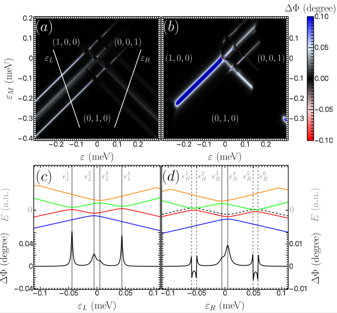
The valley degeneracy effectively creates two copies of the charge states which are coupled by the valley non-conserving tunnel amplitudes. Therefore, instead of a single anti-crossing between charge states we expect to see four anti-crossings [36]. In Fig. 2 (a) the phase shift of the cavity signal for the single electron is shown as a function of the two detuning parameters . At the (1,0,0)-(0,1,0) and the (0,0,1)-(0,1,0) charge transitions we see the splitting of a single line into three and five distinct lines. A cut along the left-center detuning shows in comparison to the level diagram that the phase responses directly match the corresponding valley splittings [see Fig. 2 (c)]. We observe a phase response (peak) at , , , and .
A cut along the right-center detuning shows a very similar phase response [see Fig. 2 (d)]. We observe a phase response (peak) at and . However, there is no phase response at but instead two phase responses (each a sharp dip followed by a sharp peak) at , and , (simulation parameters are listed in appendix C). This splitting into two signals appears if the energy splitting at the avoided crossing is smaller than the resonator frequency, . The microwave resonator becomes resonant with the ground-state excited-state transition at exactly two points [see crossing between dashed and solid lines in Fig. 2 (d)]. For small tunnel couplings the left anti-crossing between the first and second excited state in Fig. 2 (d) can be approximated by an isolated two-level system with energy splitting
| (55) |
where is the position in detuning space. From the equation above it follows that . Similarly, we find the position of the right anti-crossing between the first and second excited state at .
In total we extract the valley splittings , , and which are roughly smaller than the input settings , , and . We attribute this small systematic error to a deformation of the energy levels due to the mixing of the different levels via tunneling. To mitigate these kind of errors the cuts along and can be performed further away from the triple point, where all three charge configurations intersect. Note that we assumed an electron temperature to occupy the excited states and see features of the excited valley states in Fig. 2 (a). The phase response of the cold simulation with but applied bias between the two leads shows similar features [see Fig. 2 (b)] in the vicinity of the triple point. However, there is only a small energy window in which a finite charge current is possible [40] and higher lying valley states have a finite occupation probability. At the relevant (1,0,0)-(0,1,0) and the (0,0,1)-(0,1,0) charge transitions the charge current is blocked suppressing any probe signal from higher states (see appendix B). An alternative measurement scheme for small temperature is discussed in the next subsection.
The extraction of the valley phase is a more challenging task. Following the procedure in Ref. [32] the valley phase can be estimated by fitting the amplitudes of the phase response for the avoided crossings at , , , and in Fig. 2 (c) to the tunnel couplings and . Unfortunately, the fitting includes two more unknown parameters (taking into account charge noise) making the fits hard and unstable. Furthermore, this method requires large tunnel couplings with to gain a single response signal which for our parameter setting is not fulfilled for the (0,1,0)-(0,0,1) charge transition. Then the tunnel coupling strength and can be extracted by fitting to the energy gap. For small tunnel amplitudes Eq. (58) provides a sufficient approximation. Alternatively, for a frequency tunable resonator [35] the tunnel couplings can be extracted using spectroscopy by observing the splitting of the signal into two signals mentioned above. Using Eqs. (28)-(31) the two valley phases are given by and .
The methods introduced here do not provide a way to measure the valley angle between the left and right valley pseudo-spin . In our simplified picture for the tunneling between the dots, a direct tunnel matrix element between the left and right dot is set to zero which is close to the real scenario for a linear array. For a triangular geometry of the triple dot all tunnel matrix elements are finite and the remaining valley phase difference can be directly measured by performing the same type of measurement to extract and at the (1,0,0)-(0,0,1) charge transition. This requires the comparison of the tunnel couplings and . Furthermore, we note that in the presence of a triangular geometry a closed path can give rise to a non-vanishing geometric phase. This can in principle also be used to probe the valley in a complementary way.
| max | |||
| max | |||
| max | |||
| max |
2.1.2 Finite bias at low temperature
Instead of the two-step measurement to extract the energy spectrum from cuts through the (1,0,0)-(0,1,0) and (0,1,0)-(0,0,1) charge configurations discussed above, an investigation of the charge intersection point (1,0,0)-(0,1,0)-(0,0,1) yields the same information about the valley splitting. This is especially interesting for measurements at low temperatures since the fine-structure of cuts through (1,0,0)-(0,1,0) and (0,1,0)-(0,0,1) charge transitions is invisible in the spectroscopic data due to the blocked charge current while current flow near the triple intersection points populates the necessary excited valley states (see appendix B). Considering the same setup as above there are copies of the triple intersection point (1,0,0)-(0,1,0)-(0,0,1) due to the presence of the valley degree of freedom. The location of the intersection points in detuning space are shown in Table 1 together with an approximate energy necessary to populate the corresponding states. Each triple intersection point can be approximated for by the three-level system with eigenenergies
| (56) | ||||
| (57) | ||||
| (58) |
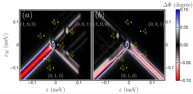
where and depending on the intersection point. Close to these points the three-level system forms a coupled two-level system between the states and with the third state lying in the middle, where denotes the eigenstate with eigenenergy . The three-level system posses a large electric quadrupole between the eigenstates and [48, 49]; all dipole moments are suppressed due to symmetry. Therefore, a symmetric architecture of the TQD resonator system, i.e, connecting the resonator via the center gate, is advantageous for probing these triple points. The probe frequency is ideally set to .
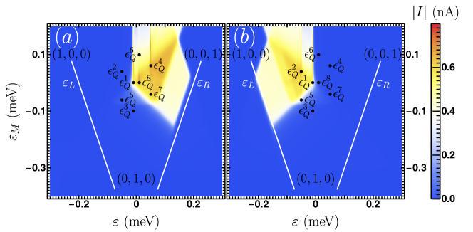
Fig. 3 shows the phase response of the probe signal in the vicinity of triple points for (a) and (b) . For an extraction of all three valley splittings a minimum of three triple points are necessary. If not enough features are visible in the phase response reversing the direction of the charge current helps to locate the position of missing triple intersection points. We see clearly a response in the phase at , , , and . In total we extract with this method the valley splittings , , and which are roughly larger than the input settings , , and . We again attribute this error to a deformation of the energy levels due to the mixing of the different levels via tunneling and the broadening of the response signal.
2.2 Three electrons in a triple quantum dot
In practice studying the three-electron case is more interesting since it allows one to measure the valley splitting and valley phase in the same charge configuration regime spin qubits can be implemented, i.e., three spin- qubits or a exchange-only qubit are implemented in the (1,1,1) charge regime. The total Hamiltonian of the three-electron case is given by
| (59) |
which can be obtained from the Hamiltonian (18) with . Focusing only on the (2,0,1), (1,1,1), and (1,0,2) charge configuration regime where the resonant exchange (RX) qubit is typically realized, the charge Hamiltonian can be simplified to
| (60) |
containing the electrostatic interactions from the capacitor model. The detuning parameters and are (up to a constant energy shift) identical to Eqs. (50) and (51). We choose the average detuning such that the TQD is occupied by three electrons. The left-center and right-center detuning parameters, and , then allow us to investigate the (2,0,1)-(1,1,1) and (1,0,2)-(1,1,1) charge transitions. Analogously to the single-electron case, the dynamics is effectively reduced to an DQD filled with two electrons.
2.2.1 Extracting the valley splitting and phase
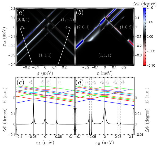
The valley degeneracy effectively creates eight copies of the charge states, two from the valley DOF in each dot for the (1,1,1) configuration and two copies for the (2,0,1) and (1,0,2) configuration neglecting the spin. These states are coupled by the valley non-conserving tunnel matrix elements. Therefore, instead of a single anti-crossing between charge states we expect to see (in the ideal case) 16 anti-crossings between the (2,0,1)-(1,1,1) and (1,0,2)-(1,1,1) charge states. Of course, to observe all crossings requires a temperature or bias such that the excited states are populated. In Fig. 4 (a) and (b) the phase shift of the cavity signal for three electrons is shown as a function of the two detuning parameters . At the (2,0,1)-(1,1,1) and the (1,0,2)-(1,1,1) charge transitions we could potentially see the splitting of a single line into multiple lines. The asymmetry in brightness between the (2,0,1)-(1,1,1) and the (1,0,2)-(1,1,1) charge transitions is due to different energy detunings for the left and right charge transitions.
A cut along the left-center detuning provides information about the level splittings [see Fig. 4 (c)]. The ground state in the (1,1,1) regime is a polarized valley state, where all electrons occupy the lower valley state, and in the (2,0,1) charge regime the two electrons form a valley-singlet state and the remaining electron in the right dot occupies the ground state. The respective energy level crossing occurs at . From Fig. 4 (c) we find , , and which are all consistent with the extracted valley splitting in the single electron case.
A cut along the right-center detuning between (1,0,2) and (1,1,1) charge states shows similar features [see Fig. 4 (d)]. The respective energy crossing occurs at and we find again two surrounding peaks at and . From Fig. 4 (d) we find , , and . This matches with the results in the single electron case.
Unfortunately, further energy crossings are hardly visible for our choice of simulation parameters in the case of three electrons, thus, we refrain from a further analysis.
3 Conclusion
In this paper we have theoretically investigated the response signal of a probed microwave resonator coupled to a linearly arranged triple quantum dot via the center dot gate electrode. A realistic model of the TQD is used in our analysis which includes electrostatic cross-talk between the dots and gates via a capacitor model, valley and spin effects, and the solution of a Redfield master equation to find the occupation probabilities. We show that a setup consisting of a TQD filled with a single electron can be used to extract important information from the TQD system such as the valley splitting and the valley phase. The accuracy of the extracted valley splitting and phase becomes higher and the interpretation simpler if the TQD is detuned such that one chemical potential is significantly increased which reduces the triple dot system to an effective double dot. A setup consisting of three electrons in a triple quantum dot is in principle capable to deliver the same information but the larger number of energy levels makes the population of the relevant excited valley states and the corresponding interpretation of the signal more difficult.
Appendix A Secular approximation
In order to compute the occupation of the energy levels we relied on the secular approximation. However, since we have no all-to-all coupling there are energy levels which do not form an anti-crossing. At these points the energy splitting goes to zero, , thus, violating the secular approximation. The validity of our calculation, however, is unaffected since the ratio between the number of valid points and detected violations is small for large sample sizes , . In all simulation we have used sample points.
Appendix B Charge current
As discussed in Ref. [36], excited energy states required for read-out of all relevant system parameters can be populated either by increasing the temperature in the system or by applying a dc bias voltage. While precise control over the temperature is experimentally challenging, biasing the left and right leads is not. The charge current from left to right can be given in two equivalent forms due to continuity
| (61a) | |||||
| (61b) | |||||
where summations run for all and . The expressions for a charge current from right to left is similar. Fig. 5 shows the charge current for . A finite current is only possible at charge quadruple points [40] where four charge configurations intersect which in our case is in the vicinity of the triple intersection points .
Appendix C Simulation parameters
For the simulation in the main text we use the following parameters from experiments in undoped Si/SiGe performed in a triple quantum dot using the gate layout described in Ref. [50]. The extracted capacitance matrix consisting of the electrostatic capacitances between the dots reads
| (65) |
and the extracted capacitance matrix consisting of the electrostatic capacitances between the dots and the gates reads
| (69) |
The capacitance matrix consisting of the electrostatic capacitances between the dots and the leads is set to
| (73) |
All capacitances are given in units of (aF) attofarad.
The remaining parameters for the simulation are the tunneling couplings, and , between the dots, the valley-orbit parameters in each dot , the incoherent decay rates and , and the charge dephasing rate . The tunneling parameters used in all simulations in the main text are chosen to be and . For the valleys splittings we use , , and . The relative valley phases , , and , where the last phase is undetectable in a linear aligned triple quantum dot. The decay and dephasing rates are set to , , and .
References
- [1] Zwanenburg F A, Dzurak A S, Morello A, Simmons M Y, Hollenberg L C L, Klimeck G, Rogge S, Coppersmith S N and Eriksson M A 2013 Rev. Mod. Phys. 85(3) 961
- [2] Watzinger H, Kukučka J, Vukušić L, Gao F, Wang T, Schäffler F, Zhang J J and Katsaros G 2018 Nature Communications 9 3902
- [3] Eich M, Pisoni R, Pally A, Overweg H, Kurzmann A, Lee Y, Rickhaus P, Watanabe K, Taniguchi T, Ensslin K and Ihn T 2018 Nano Letters 18 5042–5048 URL https://doi.org/10.1021/acs.nanolett.8b01859
- [4] Overweg H, Knothe A, Fabian T, Linhart L, Rickhaus P, Wernli L, Watanabe K, Taniguchi T, Sánchez D, Burgdörfer J, Libisch F, Fal’ko V I, Ensslin K and Ihn T 2018 Phys. Rev. Lett. 121(25) 257702 URL https://link.aps.org/doi/10.1103/PhysRevLett.121.257702
- [5] Joyce B A 1993 Handbook on semiconductors, volume 1: Basic properties of semiconductors, 2nd ed. vol 5 URL https://onlinelibrary.wiley.com/doi/abs/10.1002/adma.19930051122
- [6] Friesen M, Chutia S, Tahan C and Coppersmith S N 2007 Phys. Rev. B 75(11) 115318
- [7] Culcer D, Cywiński L, Li Q, Hu X and Das Sarma S 2009 Phys. Rev. B 80(20) 205302
- [8] Culcer D, Cywiński L, Li Q, Hu X and Das Sarma S 2010 Phys. Rev. B 82(15) 155312
- [9] Veldhorst M, Ruskov R, Yang C H, Hwang J C C, Hudson F E, Flatté M E, Tahan C, Itoh K M, Morello A and Dzurak A S 2015 Phys. Rev. B 92(20) 201401
- [10] Boross P, Széchenyi G, Culcer D and Pályi A 2016 Phys. Rev. B 94(3) 035438
- [11] Zimmerman N M, Huang P and Culcer D 2017 Nano Lett. 17 4461–4465
- [12] Gamble J K, Harvey-Collard P, Jacobson N T, Baczewski A D, Nielsen E, Maurer L, Montaño I, Rudolph M, Carroll M S, Yang C H, Rossi A, Dzurak A S and Muller R P 2016 Applied Physics Letters 109 253101
- [13] Tariq B and Hu X arXiv:1904.11944 URL https://arxiv.org/abs/1904.11944
- [14] Loss D and DiVincenzo D P 1998 Phys. Rev. A 57(1) 120
- [15] Veldhorst M, Yang C H, Hwang J C C, Huang W, Dehollain J P, Muhonen J T, Simmons S, Laucht A, Hudson F E, Itoh K M, Morello A and Dzurak A S 2015 Nature (London) 526 410–414
- [16] Zajac D M, Sigillito A J, Russ M, Borjans F, Taylor J M, Burkard G and Petta J R 2018 Science 359 439–442 ISSN 0036-8075 URL http://science.sciencemag.org/content/359/6374/439
- [17] Watson T F, Philips S G J, Kawakami E, Ward D R, Scarlino P, Veldhorst M, Savage D E, Lagally M G, Friesen M, Coppersmith S N, Eriksson M A and Vandersypen L M K 2018 Nature (London) 555 633
- [18] Yang C H, Leon R C C, Hwang J C C, Saraiva A, Tanttu T, Huang W, Camirand Lemyre J, Chan K W, Tan K Y, Hudson F E, Itoh K M, Morello A, Pioro-Ladrière M, Laucht A and Dzurak A S arXiv:1902.09126 URL https://ui.adsabs.harvard.edu/#abs/2019arXiv190209126Y
- [19] Taylor J M, Srinivasa V and Medford J 2013 Phys. Rev. Lett. 111(5) 050502
- [20] Russ M and Burkard G 2017 J. Phys. Condens. Matter 29 393001
- [21] Sala A and Danon J 2018 Phys. Rev. B 98(24) 245409 URL https://link.aps.org/doi/10.1103/PhysRevB.98.245409
- [22] Russ M, Petta J R and Burkard G 2018 Phys. Rev. Lett. 121 177701 URL https://link.aps.org/doi/10.1103/PhysRevLett.121.177701
- [23] Hada Y and Eto M 2003 Phys. Rev. B 68(15) 155322 URL https://link.aps.org/doi/10.1103/PhysRevB.68.155322
- [24] Lim W H, Zwanenburg F A, Huebl H, Möttönen M, Chan K W, Morello A and Dzurak A S 2009 Applied Physics Letters 95 242102 URL https://doi.org/10.1063/1.3272858
- [25] Xiao M, House M G and Jiang H W 2010 Applied Physics Letters 97 032103 URL https://doi.org/10.1063/1.3464324
- [26] Lim W H, Yang C H, Zwanenburg F A and Dzurak A S 2011 Nanotechnology 22 335704 URL http://stacks.iop.org/0957-4484/22/i=33/a=335704
- [27] Borselli M G, Ross R S, Kiselev A A, Croke E T, Holabird K S, Deelman P W, Warren L D, Alvarado-Rodriguez I, Milosavljevic I, Ku F C, Wong W S, Schmitz A E, Sokolich M, Gyure M F and Hunter A T 2011 Applied Physics Letters 98 123118 URL http://scitation.aip.org/content/aip/journal/apl/98/12/10.1063/1.3569717
- [28] Mi X, Cady J V, Zajac D M, Stehlik J, Edge L F and Petta J R 2017 Applied Physics Letters 110 043502
- [29] Bruhat L E, Cubaynes T, Viennot J J, Dartiailh M C, Desjardins M M, Cottet A and Kontos T 2018 Phys. Rev. B 98(15) 155313 URL https://link.aps.org/doi/10.1103/PhysRevB.98.155313
- [30] Samkharadze N, Bruno A, Scarlino P, Zheng G, DiVincenzo D P, DiCarlo L and Vandersypen L M K 2016 Phys. Rev. Applied 5(4) 044004
- [31] Stockklauser A, Scarlino P, Koski J V, Gasparinetti S, Andersen C K, Reichl C, Wegscheider W, Ihn T, Ensslin K and Wallraff A 2017 Phys. Rev. X 7(1) 011030
- [32] Mi X, Péterfalvi C G, Burkard G and Petta J R 2017 Phys. Rev. Lett. 119(17) 176803
- [33] Mi X, Benito M, Putz S, Zajac D M, Taylor J M, Burkard G and Petta J R 2018 Nature (London) 555 599 URL http://dx.doi.org/10.1038/nature25769
- [34] Samkharadze N, Zheng G, Kalhor N, Brousse D, Sammak A, Mendes U C, Blais A, Scappucci G and Vandersypen L M K 2018 Science 359 1123 URL http://science.sciencemag.org/content/359/6380/1123.abstract
- [35] Landig A J, Koski J V, Scarlino P, Mendes U C, Blais A, Reichl C, Wegscheider W, Wallraff A, Ensslin K and Ihn T 2018 Nature 560 179 URL https://doi.org/10.1038/s41586-018-0365-y
- [36] Burkard G and Petta J R 2016 Phys. Rev. B 94(19) 195305
- [37] Yang C H, Lim W H, Lai N S, Rossi A, Morello A and Dzurak A S 2012 Phys. Rev. B 86 115319 URL https://doi.org/10.1103/PhysRevB.86.115319
- [38] Zajac D M, Hazard T M, Mi X, Nielsen E and Petta J R 2016 Phys. Rev. Applied 6(5) 054013
- [39] van der Wiel W G, De Franceschi S, Elzerman J M, Fujisawa T, Tarucha S and Kouwenhoven L P 2002 Rev. Mod. Phys. 75(1) 1–22
- [40] Schröer D, Greentree A D, Gaudreau L, Eberl K, Hollenberg L C L, Kotthaus J P and Ludwig S 2007 Phys. Rev. B 76(7) 075306 URL http://link.aps.org/doi/10.1103/PhysRevB.76.075306
- [41] Ruskov R, Veldhorst M, Dzurak A S and Tahan C 2018 Phys. Rev. B 98(24) 245424 URL https://link.aps.org/doi/10.1103/PhysRevB.98.245424
- [42] Tagliaferri M L V, Bavdaz P L, Huang W, Dzurak A S, Culcer D and Veldhorst M 2018 Phys. Rev. B 97(24) 245412 URL https://link.aps.org/doi/10.1103/PhysRevB.97.245412
- [43] Breuer H P and Petruccione F 2007 The Theory of Open Quantum Systems (OUP Oxford) ISBN 978-0-19-921390-0
- [44] Collett M J and Gardiner C W 1984 Phys. Rev. A 30 1386–1391
- [45] Kulkarni M, Cotlet O and Türeci H E 2014 Phys. Rev. B 90(12) 125402 URL https://link.aps.org/doi/10.1103/PhysRevB.90.125402
- [46] Benito M, Mi X, Taylor J M, Petta J R and Burkard G 2017 Phys. Rev. B 96(23) 235434
- [47] Kohler S 2018 Phys. Rev. A 98(2) 023849 URL https://link.aps.org/doi/10.1103/PhysRevA.98.023849
- [48] Friesen M, Ghosh J, Eriksson M A and Coppersmith S N 2017 Nat. Commun. 8 15923
- [49] Koski J V, Landig A J, Russ M, Abadillo-Uriel J C, Scarlino P, Kratochwil B, Reichl C, Wegscheider W, Burkard G, Friesen M, Coppersmith S N, Wallraff A, Ensslin K and Ihn T arXiv:1905.00846 URL https://ui.adsabs.harvard.edu/abs/2019arXiv190500846K
- [50] Zajac D M, Hazard T M, Mi X, Wang K and Petta J R 2015 Applied Physics Letters 106 223507