Negative Fermi-level Pinning Effect of Metal/n-GaAs(001) Junction with Graphene Interlayer
Abstract
It is demonstrated that the electric dipole layer due to the overlapping of electron wavefunctions at metal/graphene contact results in negative Fermi-level pinning effect on the region of GaAs surface with low interface-trap density in metal/graphene/n-GaAs(001) junction. The graphene interlayer takes a role of diffusion barrier preventing the atomic intermixing at interface and preserving the low interface-trap density region. The negative Fermi-level pinning effect is supported by the Schottky barrier decreasing as metal work-function increasing. Our work shows that the graphene interlayer can invert the effective work-function of metal between and , making it possible to form both Schottky and Ohmic-like contacts with identical (particularly work-function) metal electrodes on a semiconductor substrate possessing low surface-state density.
I I. INTRODUCTION
The interfacial physics and chemistry are key elements in understanding the electrostatic environment and the associated carrier transport at metal/graphene interface. The change of electrostatic potential across metal/graphene interface is determined by not only the electron transfer between metal and graphene caused by the difference in work-function but also the formation of an electric dipole layer originating from the off-centric distribution of interacting electrons at the interface DopingGraphene1 ; DopingGraphene2 ; DopingGraphene3 . The electrical properties of metal/graphene and graphene/semiconductor contacts have been studied actively as separate physical systems GrapheneContacts1 ; GrapheneContacts2 . However, the charge carrier transport across metal/graphene/semiconductor junction as a whole, particularly taking into account the interaction dipole charges at metal/graphene contact, has not received proper attention. The interests in metal/graphene/semiconductor junction stem mainly from the possibility of modulating the electron energy barrier at interface with the graphene interlayer InterfaceGraphene1 ; InterfaceGraphene2 ; InterfaceGraphene3 ; InterfaceGraphene4 ; InterfaceGraphene5 . Recently, it has been reported that the atomically-impermeable and electronically-transparent properties of graphene inserted at metal/n-Si(001) junctions can be used to form an intact Schottky contact and investigate the interface Fermi-level pinning effect InterfaceGraphene1 . The graphene interlayer prevents the interface intermixing of metal and semiconductor atoms which occurs on the region of Si surface with very thin or no native oxide layers and leads to the formation of small-area patches with low local Schottky barriers. In this study, the graphene layer inserted at metal/n-GaAs(001) junction is found to bring about a different phenomenon although it still plays a role of diffusion barrier. It is known that the reconstructed surface of III-V compound semiconductor contains generally a low density of surface states within its band gap unless the surface structure gets compromised by some extrinsic factors including defects, oxidation, and atomic intermixing with other materials SurfacesInterfacesofElectronicMaterials . Accordingly, the regions on the surface of our GaAs(001) substrate with very thin or no native oxide layer is considered also to possess a relatively low density of surface states. However, the material intermixing on those low-surface-state regions, occurring during metal deposition, can induce a substantial amount of interface-trap states similarly to the region of GaAs surface with normal native oxides. Then, the entire region of metal/n-GaAs(001) junction will be under relatively strong interface Fermi-level pinning effect. On the other hand, if a graphene layer is inserted at metal/n-GaAs(001) interface, the material intermixing on the regions with very thin or no native oxide layer no longer occurs and thus those regions can stay with a small density of interface-trap states, bearing pretty weak Fermi-level pinning LowDit1 ; LowDit2 ; LowDit3 ; LowDit4 ; LowDit5 ; LowDit6 . From the growth mechanism of native oxide, the regions with low interface-trap density will be small in size and randomly scattered on the GaAs surface. Due to the strong Fermi-level pinning on the prevailing surrounding area, the metal-dependent variation of current-voltage (I-V) characteristics of metal/graphene/GaAs junction is expected to originate from the small patches of low interface-trap density TungPaper ; PC .
II II. EXPERIMENTAL SECTION
II.1 A. Device Fabrication
The metal/GaAs and metal/graphene/GaAs junctions were prepared as follows. The Si-doped n-type ( 5 cm-3) GaAs wafer grown by the vertical gradient freeze (VGF) method was purchased from the MTI Corporation. The GaAs substrate was first etched in a 1:1 NH4OH:H2O solution for 1 min followed by DI water rinsing Wet . After that, Ti/Pt/Au (50/200/5000 Å) ohmic contacts were formed near the edge of GaAs substrate by using e-beam evaporation and rapid thermal annealing at 400 ∘C for 300 sec Ohmic . The sample was treated in a 1:1 NH4OH:H2O etching solution for 3 min followed by DI water rinsing again right before the graphene transfer. The monolayer graphene synthesized on a Cu foil with chemical vapor deposition (CVD) was purchased from the Graphene Supermarket. In order to minimize the trapping of water molecules between graphene and GaAs surface and the residues during the transfer process Semi-Dry Transfer , we used the dry transfer method adopting thermal release tapes. The graphene layer was partially transferred on the GaAs surface in order to form metal/GaAs and metal/graphene/GaAs junctions simultaneously on the same GaAs substrate. The structural qualities of transferred graphene were examined with Raman spectrum measurements (see Supporting Information for the Raman spectrum measurements) Raman . After the graphene transfer, circular metal electrodes (Al, Ti, Ni, and Pt) of average diameter 500 m were deposited through a shadow mask on the sample surface by using e-beam evaporation. The metal/GaAs junctions were formed on the graphene-uncovered area. Finally, the graphene uncovered by metal electrodes was removed with reactive ion etching (RIE) to isolate each junction.
II.2 B. Current-Voltage Measurement
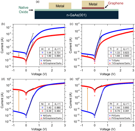
The schematic of metal/GaAs junctions with and without a graphene interlayer is illustrated in Figure 1a. Figure 1b-e show the I-V characteristics of metal/GaAs and metal/graphene/GaAs junctions. As shown in Figure 1b,c, the Al/graphene/GaAs and Ti/graphene/GaAs junctions possess the typical rectifying characteristics. In fact, their reverse bias currents are somewhat smaller (more rectifying) than the Al/GaAs and Ti/GaAs junctions. On the other hand, the reverse bias currents of Ni/graphene/GaAs and Pt/graphene/GaAs junctions are significantly larger than those of Ni/GaAs and Pt/GaAs junctions (Figure 1d,e). The rectifying behaviors of both junctions have almost disappeared, turning into Ohmic-like ones. This is quite counter-intuitive since the local Schottky barrier formed on the region of GaAs surface with low interface-trap density is expected to be low for Al/graphene/GaAs and Ti/graphene/GaAs junctions and high for Ni/graphene/GaAs and Pt/graphene/GaAs junctions when considering the difference in metal work-function.
II.3 C. Internal Photoemission Measurement
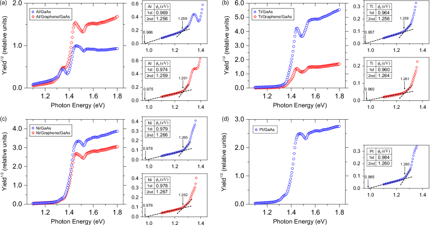
The Internal Photoemission (IPE) yield spectra InterfaceGraphene1 ; IPE ; AuGaAsIPE for metal/GaAs and metal/graphene/GaAs junctions are shown in Figure 2. Since the IPE measurement reveals the motion of ballistic electron across the junction interface, its signals will be contributed collectively by all regions in the junction. However, if a junction is mostly uniform and only a small areal fraction of isolated patches exists with their interface energy barriers different from those on the uniform surrounding region, the IPE spectrum will be dominated by the prevailing region and the contribution from the small patches will be almost invisible. In the IPE spectra of metal/GaAs junctions, two thresholds for the conduction band minima ( and valleys) of GaAs Valley are clearly observed. The first threshold represents the commonly accepted Schottky barrier of metal/GaAs junction, which reflects the electron transmission from metal into the valley in GaAs. The additional transmission into the valley in GaAs corresponds to the second threshold. The gap between first and second thresholds is about 0.29 eV, which is in excellent agreement with the known energy separation between and valleys. However, the observation of additional transmission into the valley of GaAs is disturbed by the humps of IPE yield around 1.33 eV Localized (see Supporting Information for details on the direct optical excitation from localized interface states). Since the two thresholds are extracted to be pretty much identical for all four metal electrodes (Al, Ti, Ni, Pt) and no signature for additional threshold is observed, the Fermi-level pinning can be concluded to be strong uniformly throughout the entire metal/GaAs junction as known well. The metal/graphene/GaAs junctions also show two common thresholds in their IPE spectra for Al, Ti, and Ni electrodes which are quite similar to those for the metal/GaAs junctions. In case of Pt/graphene/GaAs junction, the large leakage current, confirmed in the I-V curve (Figure 1e), overwhelmed the photocurrent completely so that we could not determine the corresponding IPE yield at all (Figure 2d). The similarity in the IPE thresholds of metal/graphene/GaAs junction for different metal electrodes implies that the Fermi-level pinning is strong in the vast majority of junction area where the regular oxide layer is expected to reside and bear high interface-trap density. Here, there are several things to note about characterizing the fabricated junctions. All transport measurements including I-V and IPE measurements were carried out at room temperature. The power of incident light was measured separately by using a photodiode, HAMAMATSU S2281-04 (Si photodiode for the wavelength of 200-1180 nm) for acquiring the quantum yield of IPEInterfaceGraphene1 ; IPE ; AuGaAsIPE . After the measurements of electrical properties, the layer structures of fabricated junctions were examined by taking transmission electron microscope (TEM) images (see Supporting Information for the TEM images) TEM ; Oxide1 ; Oxide2 .
III III. RESULTS AND DISCUSSION
III.1 A. Negative Fermi-level Pinning Effect
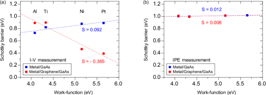
Averaged over several different junctions, the Schottky barriers of metal/GaAs and metal/ graphene/GaAs junctions were obtained from the I-V and IPE measurements. They were determined by either fitting the measured I-V curves shown in Figure 1 to the thermionic-emission theory Thermionic or extracting the first threshold of IPE yield shown in Figure 2 with the image force lowering included. Figure 3a,b show the obtained Schottky barriers of metal/GaAs and metal/graphene/GaAs junctions as a function of metal work-function . From the I-V measurements, the pinning factor , defined to be Pinning ; SzeText ; SzePaper , are obtained to be 0.092 and -0.365 for metal/GaAs and metal/graphene/GaAs junctions, respectively. As mentioned previously, it is quite interesting that the Schottky barrier of metal/graphene/GaAs junction decreases as the metal work-function increases, reflected on the negative value (-0.365) of . In normal circumstances, the pinning factor ranges between 0 and 1 depending on the pinning strength. In case of IPE measurements, the Schottky barriers for metal/GaAs and metal/graphene/GaAs junctions are extracted to be very similar to each other for all the metals except for Pt. Just as a reminder, the IPE spectrum for Pt/graphene/GaAs couldn’t be obtained due to the large junction leakage. The pinning factors in the IPE measurements are found to be 0.012 and 0.008 for metal/GaAs and metal/graphene/GaAs junctions, respectively, both indicating strong Fermi-level pinning effect.
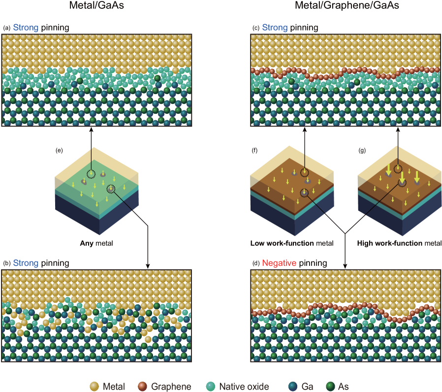
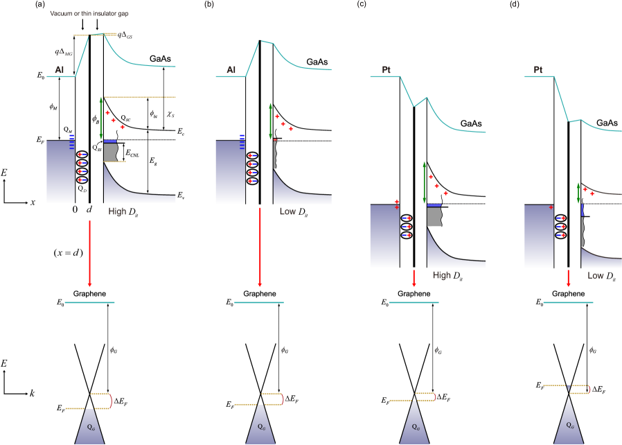
Based on the I-V and IPE measurements described above, it seems plausible to conclude the following spatial distributions for the interface Fermi-level pinning and associated current flows in metal/GaAs and metal/graphene/GaAs junctions. For metal/GaAs junctions, as shown in Figure 4a,b, the entire region of GaAs surface will have high interface-trap density due to oxidation (native oxide, Figure 4a) or material intermixing with metal atoms (Figure 4b) LowDit1 ; LowDit2 ; LowDit3 ; LowDit4 ; LowDit5 ; LowDit6 . Hence, the interface Fermi-level pinning effect will appear to be strong throughout the entire region of junction and the junction current will be distributed uniformly (Figure 4e). In case of metal/graphene/GaAs junctions, the prevailing region with regular native oxides will have a large density of interface-trap states (Figure 4c) and the Fermi-level pinning on this region will be strong similarly to the metal/GaAs junction case. Meantime, the small patches with very thin or no native oxide layer will maintain low interface-trap density thanks to the protection of graphene interlayer (Figure 4d) and the observed negative Fermi-level pinning will occur here. Due to the negative pinning, these small patches will have current flows comparable to the surrounding regions for work-function metal electrodes (Figure 4f) forming relatively high interface energy barriers. On the other hand, the current flow through the small patches will be a lot more in comparison with the surrounding regions for work-function metal electrodes (Figure 4g) bearing leaky current paths with low interface energy barriers.
III.2 B. Calculated energy band profile across junction
In order to understand the unusual negative Fermi-level pinning in the metal/graphene/GaAs junction, the electron energy band profiles across the junction were obtained by performing finite element electrostatic modeling with a commercial software package FlexPDE PDE1 ; PDE2 ; PDE3 (see Supporting Information for details on the finite element electrostatic modeling). All parameters were implemented with the values measured or reported in the literature SzeText ; GaAsDit ; CRC ; MP ; Work-function . The key variable in our modeling is the interaction dipole charge density () at metal/graphene contact which was supported by density functional theory (DFT) calculations to exist due to the off-centric distribution of the overlapped electron wavefunctions in the gap between metal and graphene layer DopingGraphene1 ; DopingGraphene2 . Here, we note that indicates the charges of interaction dipole layer on the graphene side. First of all, we have calculated the Schottky barrier () and pinning strength () for various interface-trap density () on GaAs surface by assuming = 0 in order to verify whether or not the observed negative Fermi-level pinning can occur without the interaction dipole layer. If we do not consider the interaction dipole layer, the pinning strength is always calculated to be positive for eV-1cm eV-1cm-2 which is the typical range for III-V compound semiconductors GaAsDit (see Table S1 in Supporting Information). In addition, if we estimate the to match with the I-V measured for eV-1cm-2, the increases dramatically to have the physically impossible values (see Table S2 in Supporting Information). This confirms that the negative Fermi-level pinning effect observed in the I-V measurements should occur on the region with low interface-trap density ( eV-1cm-2) as concluded from the IPE measurements. Since the interaction dipole layer at metal/graphene contact is expected to be uniformly formed throughout the entire contact, it is reasonable to assume that each metal will have a certain constant in metal/graphene/GaAs junction regardless of the locally-varying on GaAs surface. In the electrostatic modeling, we adopted the obtained for eV-1 cm-2 to fit the I-V measured and eV-1 cm-2 was used for the prevailing region with high interface-trap density. The calculated relevant potentials and charges are listed (see Table S3 in Supporting Information) and the band profiles of Al/graphene/GaAs and Pt/graphene/GaAs junctions are shown in Figure 5 as the representatives of low and high work-function metal electrodes.
III.3 C. Electronegativity difference and interaction dipole charge
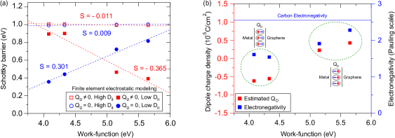
Figure 6a shows the Schottky barriers extracted from the modeling for four different combinations of and . As seen in the figure, the negative pinning factor for metal/graphene/ GaAs junction is obtained only with non-zero for low . In case of Pt/graphene/GaAs junction, it is found that should be positive to obtain the Schottky barrier measured to be small. This polarity actually coincides with the DFT calculation results mentioned previously DopingGraphene1 ; DopingGraphene2 . Meanwhile, for Al/graphene/GaAs junction is found to be negative to match with the measured Schottky barrier. According to the DFT calculations, for the Al/graphene/GaAs junction will still be positive although its magnitude becomes much smaller than that of Pt/graphene/GaAs junction. However, the positive will lower the Schottky barrier always, relative to the junction without the graphene interlayer, since the electrostatic potential drops across the gap between metal and graphene layer. Our electrostatic modeling indicates clearly that the Schottky barrier of Al/graphene/GaAs junction is quite low with zero or positive . Thus it seems inevitable for to be negative for bearing the experimentally-measured large Schottky barrier.
It is known well that the exchange correlation potential for electrons is attractive in front of a metal surface and the electrons of an atom adsorbed on the metal surface is attracted toward the metal side Exchange-Correlation . Hence, the positive is quite understandable in terms of this exchange correlation. Then, the question is what induces the negative of Al/graphene/ GaAs junction. One possibility that we can think of is the electronegativity difference between metal and carbon atom. Figure 6b shows the obtained from the electrostatic modeling and the electronegativity Electronegativity of a metal atom as a function of metal work-function. As shown in the figure, the electronegativities of all the metals used in our work are smaller than that of carbon. This implies that the interacting electrons between metal and graphene will be attracted more toward the graphene side. Especially, the electronegativities of Al and Ti with relatively low work-functions are quite small in comparison with carbon. Accordingly, the driving force shifting the interacting electrons toward the graphene side can be significant, overcoming the tendency of shifting them toward the metal side due to the exchange correlation and leading to the negative . For Ni and Pt with relatively high work-functions, the difference of electronegativity from carbon becomes smaller. Therefore, in this case, the interacting electrons are expected to be shifted toward the metal by more prominent exchange correlation so that the positive is induced. Here, it is noted that the mechanism described above is only a possibility relying on the two known factors of exchange correlation and atomic electronegativity which have been addressed independently. One point consistent between the DFT calculation and our electrostatic modeling is that the tendency of shifting the interacting electrons toward the metal side is reduced significantly for low work-function metals. However, what is apparent from the fundamental physics standpoint, supported from the electrostatic modeling, is that the sign change of is the essential requirement for the negative Fermi-level pinning observed in our experiments.
IV IV. CONCLUSIONS
In conclusion, we report the negative Fermi-level pinning effect observed experimentally in metal/graphene/n-GaAs(001) junction. The low interface-trap density regions, protected by the graphene interlayer, are found to have the local Schottky barrier affected directly by the interaction dipole layer at metal/graphene contact. In order to explain the observed negative Fermi-level pinning, it is found that the interacting electrons at the metal/graphene interface should be attracted more toward the graphene side for low work-function metals, bearing the increase of electrostatic potential across the interface. For high work-function metals, they should be attracted more toward the metal side, making the electrostatic potential decrease across the interface accordingly. Based on our work, it can be claimed that the graphene interlayer can invert the effective work-function of metal between high and low, making it possible to form both Schottky and Ohmic-like contacts with identical (particularly work-function) metal electrodes on a semiconductor substrate possessing low surface-state density.
V Author Contributions
H.H.Y and K.P. conceived and designed the experiments. H.H.Y., J.K., and K.M. fabricated the devices. H.H.Y. and W.S. performed the measurements. H.H.Y., W.S., S.J., J.K., K.M., G.C., and K.P. analyzed the measured data. W.S. and S.J. performed the electrostatic modeling. H.Y.J. and J.H.L. took TEM images. All authors discussed the results and contributed to writing the manuscript. H.H.Y. and W.S. contributed equally to this work.
VI Acknowledgements
This work was supported by Space Core Technology Development Program (2016M1A3A3A02017648), Basic Science Research Program (2016R1A2B4014762, 2019R1F1A1057767), and Global Ph.D Fellowship Program (2015H1A2A1033714) through the National Research Foundation funded from the Ministry of Science and ICT in Korea. This work has also benefited from the use of the facilities at UNIST Central Research Facilities.
References
- (1) Giovannetti, G.; et al. Doping graphene with metal contacts. Phys. Rev. Lett. 2008, 101, 4.
- (2) Khomyakov, P. A.; et al. First-principles study of the interaction and charge transfer between graphene and metals. Phys. Rev. B 2009, 79, 12.
- (3) Song, S. M.; Park, J. K.; Sul, O. J.; Cho, B. J. Determination of work Function of graphene under a metal electrode and Its role in contact resistance. Nano. Lett. 2012, 12, 3887-3892.
- (4) Allain, A.; Kang, J. H.; Banerjee, K.; Kis, A. Electrical contacts to two-dimensional semiconductors. Nat. Mater. 2015, 14, 1195-1205.
- (5) Xu, Y.; et al. Contacts between two- and three-dimensional materials: ohmic, Schottky, and p-n heterojunctions. ACS. Nano. 2016, 10, 4895-4919.
- (6) Yoon, H. H.; et al. Strong Fermi-level pinning at metal/n-Si(001) interface ensured by forming an intact Schottky contact with a graphene Insertion layer. Nano. Lett. 2017, 17, 44-49.
- (7) Byun, K. E.; et al. Graphene for true ohmic contact at metal-semiconductor junctions. Nano. Lett. 2013 13, 4001-4005.
- (8) Lee, M. H. et al. Two-Dimensional Materials Inserted at the Metal/Semiconductor Interface: Attractive Candidates for Semiconductor Device Contacts. Nano. Lett. 2018, 18, 4878-4884.
- (9) Baek, S. H. C.; et al. Alleviation of Fermi-level pinning effect at metal/germanium interface by the insertion of graphene layers. Appl. Phys. Lett. 2014, 105, 4.
- (10) Kim, W.; et al. Tunable graphene-GaSe dual heterojunction device. Adv. Mater. 2016, 28, 1845-1852.
- (11) Brillson, L. J. Surfaces and Interfaces of Electronic Materials; John Wiley & Sons, 2010; Vol. 7.
- (12) Drummond, T. J. Schottky barriers on GaAs: screened pinning at defect levels. Phys. Rev. B 1999, 59, 8182-8194.
- (13) Altuntas, H.; Altindal, S.; Ozcelik, S.; Shtrikman, H. Electrical characteristics of Au/n-GaAs Schottky barrier diodes with and without SiO2 insulator layer at room temperature. Vacuum 2009, 83, 1060-1065.
- (14) Flores, F.; Perez, R.; Rincon, R.; Saizpardo, R. Electron-states at semiconductor interfaces - the intrinsic and extrinsic charge neutrality levels. Philos. Trans. R. Soc. Lond. Ser. A-Math. Phys. Eng. Sci. 1993, 344, 567-577.
- (15) Spicer, W. E.; Newman, N.; Spindt, C. J.; Lilientalweber, Z.; Weber, E. R. Pinning and Fermi level movement at GaAs-surfaces and interfaces. J. Vac. Sci. Technol. A-Vac. Surf. Films. 1990, 8, 2084-2089.
- (16) Cheng, C. P.; et al. Atomic nature of the Schottky barrier height formation of the Ag/GaAs(001)-2 x 4 interface: an in-situ synchrotron radiation photoemission study. Appl. Surf. Sci. 2017, 393, 294-298.
- (17) Suyatin, D. B.; et al. Strong Schottky barrier reduction at Au-catalyst/GaAs-nanowire interfaces by electric dipole formation and Fermi-level unpinning. Nat. Commun. 2014, 5, 8.
- (18) Tung, R. T. The physics and chemistry of the Schottky barrier height. Appl. Phys. Rev. 2014, 1, 54.
- (19) Tung, R. T. Electron-transport at metal-semiconductor interfaces - general-theory. Phys. Rev. B. 1992, 45, 13509-13523.
- (20) Song, J. S.; et al. Wet chemical cleaning process of GaAs substrate for ready-to-use. J. Cryst. Growth. 2004, 264, 98-103.
- (21) Rideout, V. A review of the theory and technology for ohmic contacts to group III-V compound semiconductors. Solid-State Electron. 1975, 18, 541-550.
- (22) Song, J. S.; et al. Reduction of Water-Molecule-Induced Current-Voltage Hysteresis in Graphene Field Effect Transistor with Semi-Dry Transfer Using Flexible Supporter. J. Appl. Phys. 2019, 125, 184302.
- (23) Ferrari, A. C.; et al. Raman spectrum of graphene and graphene layers. Phys. Rev. Lett. 2006, 97, 4.
- (24) Afanas’ev, V. V. Internal Photoemission Spectroscopy: Fundamentals and Recent Advances; Elsevier, 2014.
- (25) Gigli, G.; et al. Direct assessment of tunable Schottky barriers by internal photoemission spectroscopy. Appl. Phys. Lett. 1998, 73, 259-261.
- (26) Ke, M. L.; Westwood, D. I.; Matthai, C. C.; Richardson, B. E.; Williams, R. H. Hot-electron transport through Au/GaAs and Au/GaAs/AlAs heterojunction interfaces: ballistic-electron-emission-microscopy measurement and Monte Carlo simulation. Phys. Rev. B 1996, 53, 4845-4849.
- (27) Bardi, J.; Binggeli, N.; Baldereschi, A. Existence of localized interface states in metal/GaAs(100) junctions: Au versus Al contacts. Phys. Rev. B 2000, 61, 5416-5422.
- (28) Norimatsu, W.; Kusunoki, M. Structural features of epitaxial graphene on SiC {0001} surfaces. J. Phys. D-Appl. Phys. 2014, 47, 16.
- (29) Torkhov, N. A. Formation of a native-oxide structure on the surface of n-GaAs under natural oxidation in air. Semiconductors 2003, 37, 1177-1184.
- (30) Talin, A. A.; et al. Time-dependent ballistic electron-emission microscopy studies of a Au/(100)GaAs interface with a native-oxide diffusion barrier. Appl. Phys. Lett. 1993, 62, 2965-2966.
- (31) Cheung, S. K.; Cheung, N. W. Extraction of Schottky diode parameters from forward current-voltage characteristics Appl. Phys. Lett. 1986, 49, 85-87.
- (32) Dimoulas, A.; Tsipas, P.; Sotiropoulos, A.; Evangelou, E. K. Fermi-level pinning and charge neutrality level in germanium. Appl. Phys. Lett. 2006, 89, 3.
- (33) Sze, S. M.; Ng, K. K. Physics of Semiconductor Devices; John Wiley & Sons, 2006.
- (34) Cowley. A. M.; Sze, S. M. Surface states and barrier height of metal-semiconductor systems. J. Appl. Phys. 1965, 36, 3212-&.
- (35) PDE Solutions, Inc., Spokane Valley, WA, U.S.A., http://www.pdesolutions.com
- (36) Choi, G.; et al. Schottky barrier modulation of metal/4H-SiC junction with thin interface spacer driven by surface polarization charge on 4H-SiC substrate. Appl. Phys. Lett. 2015, 107, 5.
- (37) Park, K. B.; et al. Effect of inclined quantum wells on macroscopic capacitance-voltage response of Schottky contacts: Cubic inclusions in hexagonal SiC. Appl. Phys. Lett. 2005, 86, 3.
- (38) Brammertz, G.; et al. Capacitance–voltage characterization of GaAs–oxide interfaces. J. Electrochem. Soc. 2008, 155, H945.
- (39) Haynes, W. M. CRC handbook of chemistry and physics; CRC press, 2014.
- (40) Tipler, P. A.; Llewellyn, R. A. Modern physics; Freeman, 2008.
- (41) Michaelson, H. B. The work function of the elements and its periodicity. J. Appl. Phys. 1977, 48, 4729.
- (42) Da Silva, J. L. F.; Stampfl, C.; Scheffler, M. Adsorption of Xe Atoms on Metal Surfaces: New Insights from First-Principles Calculations. Phys. Rev. Lett. 2003, 90, 066104.
- (43) Pearson, R. G. Absolute electronegativity and hardness - application to inorganic-chemistry. Inorg. Chem. 1988, 27, 734-740.