Imaging doubled shot noise in a Josephson scanning tunneling microscope
Abstract
We have imaged the current noise with atomic resolution in a Josephson scanning tunneling microscope with a Pb-Pb junction. By measuring the current noise as a function of applied bias, we reveal the change from single electron tunneling above the superconducting gap energy to double electron charge transfer below the gap energy when Andreev processes become dominant. Our spatially resolved noise maps show that this doubling occurs homogeneously on the surface, also on impurity locations, demonstrating that indeed the charge pairing is not influenced by disruptions in the superconductor smaller than the superconducting coherence length.
The coupling between two macroscopic superconducting electrodes through an insulating layer can lead to a dissipationless current called Josephson supercurrent. The critical current is the maximal supercurrent that the junction can sustain; it is related to the individual superconducting order parameters in both electrodes, as well as their coupling Josephson (1963). In the zero-voltage limit, this supercurrent is carried by paired electrons (Cooper pairs), carrying twice the electron charge . Applying a bias voltage larger than twice the pair-breaking gap energy , , over the junction results in a normal current carried predominantly by quasiparticles with single electron charge (Fig. 1(b)). In the energy range below the gap edge, only so-called Andreev reflection processes can transport the quasiparticles across the junction by reflecting particles carrying opposite charge. These processes lead to effective charge transfer of multiple electron charges Blonder et al. (1982); Octavio et al. (1983); Beenakker (1997). In the energy range , the dominant process is a single Andreev reflection leading to transfer of effectively double the electron charge, as illustrated in Fig. 1(c).
One cannot tell from the time-averaged value of the current whether it is carried by multiple integers of charge, but this becomes apparent when measuring the fluctuations of the current, or in others words, the current noise Blanter and Büttiker (2000); Jehl et al. (2000); Lefloch et al. (2003); Ronen et al. (2016); Dieleman et al. (1997). In general, the noise originating from the flow of uncorrelated particles in a tunneling junction (shot noise) is a purely Poissonian process. The current noise power is then proportional to the charge and the current of the carriers, Blanter and Büttiker (2000). At lower bias voltages, when Andreev processes become relevant, the transferred charge in a Josephson junction can effectively double and the noise is also expected to be two times the Poissonian value. Spectroscopic noise measurements in mesoscopic systems have revealed such noise signatures of multiple electron charge transport in superconducting junctions associated with Andreev processes Jehl et al. (2000); Lefloch et al. (2003); Ronen et al. (2016); Dieleman et al. (1997) and fractional charges in quantum hall systems De-Picciotto et al. (1997); Saminadayar et al. (1997).
In this Letter we perform such noise spectroscopy measurements spatially resolved with atomic resolution in a Josephson scanning tunneling microscope. We use our recently developed scanning tunneling noise microscopy (STNM) technique to spatially resolve the current and its time-resolved fluctuations simultaneously with atomic resolution Bastiaans et al. (2018a). We first demonstrate the current noise doubling from single to double charge transfer below the gap edge in a junction between a superconducting Pb tip and a Pb(111) sample. We then visualize this noise enhancement by spatially mapping the effective charge transfer over the sample surface. We show that it is homogeneous over the sample surface, also including impurity locations, demonstrating that the charge pairing is not influenced by disruptions smaller than the coherence length ( nm in Pb).
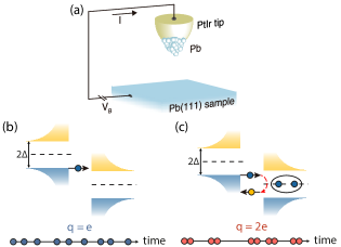
A schematic of our setup is shown in Fig. 1, where a superconducting STM tip is brought in tunneling contact with a superconducting sample to form a superconductor-insulator-superconductor (SIS) junction. We create this junction in our modified low-temperature (2.2 K) Unisoku USM-1500 STM setup. First, the Pb(111) single crystal surface is cleaned by repetitive cycles of sputtering at 1kV with an Ar pressure of mbar (background pressure mbar) and annealing. We then indent the mechanically grinded PtIr tip into the surface to decorate it with a superconducting cluster of Pb atoms until we obtain a SIS junction Ruby et al. (2015); Franke et al. (2011); Randeria et al. (2016).
To demonstrate the high quality of the SIS junction in our setup, we display its distinct spectroscopic signatures for varying normal state resistance in Fig. 2. The first signature is visible in the single particle channel, where quasiparticles with energies larger than the pair-breaking gap transfer the charge. The tunneling spectra in Fig. 2(a) show sharp coherence peaks, which are located at energies equal to the sum of both superconducting gaps of tip and sample meV. The clear U-shaped gap at 13.6 M can be used as a benchmark for bulk-like superconducting properties of the tip and, also considering the low conductance, indicates that only a single transmission channel is present Scheer et al. (1998). Due to the sharp density of states of the superconducting tip, the spectroscopic features are much sharper than one would expect from conventional thermal broadening Ruby et al. (2015). We can fit these spectra with a modified phenomenological gap equation Dynes et al. (1978) to extract the effective electron temperature of 2.2 K, which is similar to the measured phonon temperature, as electron-phonon coupling is still rather efficient at these temperatures.
The next signature stems from Andreev processes that are visible at lower junction resistances. These lead to a sub-gap structure with humps in the differential conductance. Specifically, at energies below , Andreev processes of order become possible with relative probability , where is the transparency of the junction. A small hump, indicated by the black arrows in Fig. 2 (a) and (b), is visible in the differential conductance when the order of lowest allowed Andreev reflection process changes Blonder et al. (1982); Octavio et al. (1983).
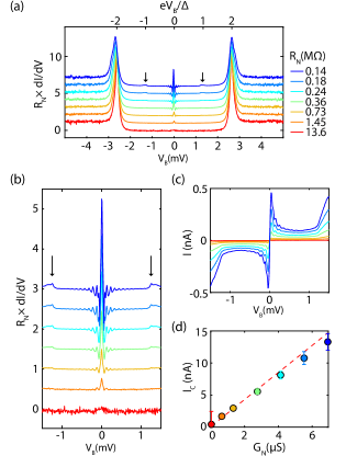
The spectroscopic signatures related to the Josephson supercurrent in the junction are observed in the differential conductance at energies close to the Fermi level : a peak that is enhanced with decreasing , and small oscillations around the central peak (Fig. 2(b)). To understand these, we first survey the energy scales in our setup. The capacitive energy and the thermal energy are larger than the Josephson energy . Therefore, the environmental impedance becomes a relevant quantity, and thermal phase fluctuations across the junction govern the Josephson current, shifting the maximum current to a non-zero bias Ingold et al. (1994). Close to the Fermi energy we access the Cooper-pair channel associated with the coupling between the two superconducting condensates. The prominent peak at in Fig. 2(b), corresponding to the local maximum in the current in Fig. 2(c), originates from the phase fluctuating Josephson current Randeria et al. (2016); Ingold et al. (1994). Both the maximum Josephson current and the differential conductance at zero bias are proportional to the square of the intrinsic critical current of the Josephson junction. The critical currents we obtain for these spectra show a linear relation with and are well consistent with the Ambegaokar-Baratoff formula (Fig. 2(d)) Ambegaokar and Baratoff (1963). We also note the small oscillating features in both the conductance and current spectra stretching far out to meV, originating from coupling of the junction with its dissipative electromagnetic environment, previously explained by a tip-induced antenna mode Randeria et al. (2016); Jäck et al. (2015).
We now want to come to the central part of our paper, where we show the visualization of the doubling of the current noise in this scanning Josephson junction using STNM. The central challenge for measuring current noise in a conventional scanning tunneling microscope (STM) is that the temporal resolution is generally limited to only a few kHz, because the combination of the high impedance () tunnel junction and capacitance of the interfacing cables ( pF) form an inherent low-pass filter. As a consequence, STM usually provides a static, time-averaged picture, lacking information about possible dynamical phenomena in the junction Chen (2008), especially when requiring atomic-resolution scanning.
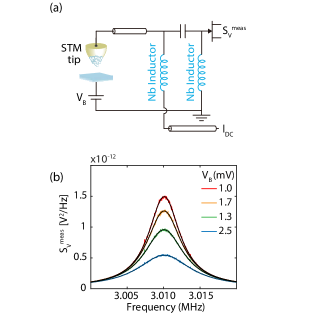
Our noise measurement apparatus, described in detail elsewhere Bastiaans et al. (2018a), builds upon earlier high-frequency STMs Birk et al. (1995); Kemiktarak et al. (2007) but is based on a superconducting LC resonating circuit that is connected to the Josephson junction, as illustrated in Fig. 3(a). Current fluctuations in the junction are converted into voltage fluctuations at resonance of the LC circuit, which are then amplified by the custom-built cryogenic amplifier Dong et al. (2014) into a 50 line. To illustrate how we extract the magnitude of the current noise in the junction, we plot several curves of the measured power spectral density in Fig. 3(b) for various bias voltages. To mitigate the effect of a non-linear differential conductance on the effective resonator impedance, one needs to separate the measured signal into the noise components Bastiaans et al. (2018a); Jabdaraghi et al. (2017). The total measured voltage noise is
| (1) |
where is the total gain of the amplification chain, the impedance of the resonating circuit and the total current noise in the circuit. The strong influence of the highly non-linear differential conductance on the total impedance of the resonator is also illustrated in Fig. 3(b), where the clear change of the measured power spectral density for varying bias voltage is due to the simultaneously changing impedance of the resonator and amplitude of the noise as function of bias.
After correcting for the non-linear differential conductance, the total current noise equals
| (2) |
where is the effective charge, is the effective temperature and is the input noise of the amplifier. The first term represents the shot noise in the junction and the second term represents the thermal noise. The black curves in Fig. 3(b) represent fitting of to the measured noise spectra, which we then use to obtain a value for the effective charge transferred across the junction.
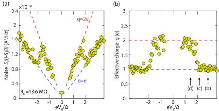
We first measure the current noise as a function of energy at a single location. Fig. 4(a) shows the measured current noise power as function of bias, with the zero-current noise subtracted to remove the thermal noise component and input noise of the amplifier: . The dashed lines indicate the theoretically calculated shot noise curves as described above, for effective charge (blue) and (red). At large bias voltage the experimental data follows the noise for single electron tunneling. However, the current noise clearly doubles from to at the coherence peak energy . We obtain the effective charge transferred by dividing the measured noise power by the full Poissonian noise (Fig. 4(b)). The clear step in effective charge as a function of applied bias at the gap energy demonstrates that the tunneling current is now effectively carried by double charge quanta due to Andreev reflection processes. This is well consistent with theoretical descriptions Blonder et al. (1982); Octavio et al. (1983); Beenakker (1997) and experimental observations in mesoscopic devices, where Andreev reflections lead to enhanced noise in nanofabricated SIS junctions Ronen et al. (2016); Dieleman et al. (1997) and short diffusive normal metal – superconductor contacts Jehl et al. (2000); Lefloch et al. (2003), but has never been seen in a STM setup or at such low transparencies. In the present project, we use transparencies of leading to a single channel of transmission, whereas in mesoscopic devices usually multiple channels of are involved.
[\capbeside\thisfloatsetupcapbesideposition=right,center,capbesidewidth=5cm]figure[\FBwidth]
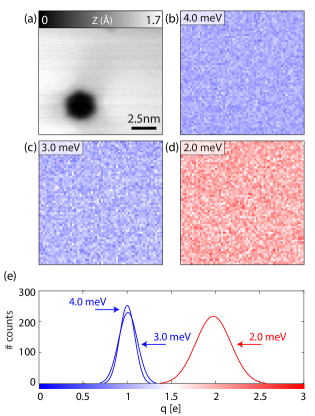
Finally, we apply the spatial mapping capabilities of our STNM setup to resolve this doubling of the noise over the sample surface with atomic-scale resolution. Figure 5(a) shows a topographic image of the Pb(111) surface in a 12,5 nm field of view, including a hexagonal shaped impurity previously identified as a sub-surface Ar nanocavity Müller et al. (2016). We performed the noise-spectroscopy measurement in the same field of view by scanning the tip over the surface while simultaneously measuring the current noise. The spatially resolved noise maps at various bias voltages shown in Fig. 5 (b-d), exhibit a homogeneous contrast at energies above the pair-breaking gap energy, as is expected for transfer of uncorrelated particles. Below the superconducting gap energy we again observe homogeneous contrast, but now at an elevated value of the noise power around an effective charge equal to . While we observe a strong contrast in the topography, these spatially resolved noise maps show that the doubling occurs homogeneously over the surface, also on the location of the nanocavity. This demonstrates that disruptions in the superfluid, due to possible charge confinement or scattering on the nanocavity Müller et al. (2016), on length scales smaller than the superconducting coherence length ( nm in Pb) do not influence the charge pairing, since the spatially resolved current noise is unaffected.
In summary, we measured doubled shot noise caused by Andreev reflections in a Josephson scanning tunneling microscope using noise spectroscopy measurements. We spatially resolved this doubling with atomic-scale resolution on the surface of the conventional superconductor Pb(111). The ability to spatially resolve the charge dynamics with such precision opens new paths for investigating many-body correlation effects in quantum materials. Recently, it led to a novel understanding of cuprate high-temperature superconductors, where the discovery of charge trapping dynamics suggests a picture of copper-oxide planes separated by thin insulating layers within the three-dimensional superconducting state Bastiaans et al. (2018b); Massee et al. (2019). Potentially, atomically resolved noise measurements will also reveal new insight in fluctuating stripe order Carlson et al. (2006) and pre-formed pairing in the pseudogap regime Lee (2014); Keimer et al. (2015), Kondo effects in heavy fermion systems Figgins and Morr (2010), or signatures of Majorana modes in one-dimensional wires on a superconducting surface Nadj-Perge et al. (2014).
Acknowledgements.
We acknowledge T. Benschop, Y.M. Blanter, V. Cheianov, T.M. Klapwijk, F. Massee, D.K. Morr, K. van Oosten, M.T. Randeria and J.M. van Ruitenbeek for valuable discussions. This work was supported by the European Research Council (ERC StG SpinMelt) and by the Netherlands Organization for Scientific Research (NWO/OCW), as part of the Frontiers of Nanoscience program, as well as through a Vidi grant (680-47-536).References
- Josephson (1963) B. D. Josephson, Physics Letters 1, 251 (1963).
- Blonder et al. (1982) G. E. Blonder, M. Tinkham, and T. M. Klapwijk, Physical Review B 25, 4515 (1982).
- Octavio et al. (1983) M. Octavio, M. Tinkham, G. E. Blonder, and T. M. Klapwijk, Physical Review B 27, 6739 (1983).
- Beenakker (1997) C. Beenakker, Reviews of Modern Physics 69, 731 (1997).
- Blanter and Büttiker (2000) Y. Blanter and M. Büttiker, Physics Reports 336, 1 (2000).
- Jehl et al. (2000) X. Jehl, M. Sanquer, R. Calemczuk, and D. Mailly, Nature 405, 50 (2000).
- Lefloch et al. (2003) F. Lefloch, C. Hoffmann, M. Sanquer, and D. Quirion, Physical Review Letters 90, 067002 (2003).
- Ronen et al. (2016) Y. Ronen, Y. Cohen, J.-H. Kang, A. Haim, M.-T. Rieder, M. Heiblum, D. Mahalu, and H. Shtrikman, PNAS 113, 1743 (2016).
- Dieleman et al. (1997) P. Dieleman, H. Bukkems, T. Klapwijk, M. Schicke, and K. Gundlach, Physical Review Letters 79, 3486 (1997).
- De-Picciotto et al. (1997) R. De-Picciotto, M. Reznikov, M. Heiblum, V. Umansky, G. Bunin, and D. Mahalu, Nature 389, 162 (1997).
- Saminadayar et al. (1997) L. Saminadayar, D. C. Glattli, Y. Jin, and B. Etienne, Physical Review Letters 79, 2526 (1997).
- Bastiaans et al. (2018a) K. M. Bastiaans, T. Benschop, D. Chatzopoulos, D. Cho, Q. Dong, Y. Jin, and M. P. Allan, Review of Scientific Instruments 89, 093709 (2018a).
- Ruby et al. (2015) M. Ruby, B. W. Heinrich, J. I. Pascual, and K. J. Franke, Physical Review Letters 114, 157001 (2015).
- Franke et al. (2011) K. J. Franke, G. Schulze, and J. I. Pascual, Science 332, 940 (2011).
- Randeria et al. (2016) M. T. Randeria, B. E. Feldman, I. K. Drozdov, and A. Yazdani, Physical Review B 93, 161115(R) (2016).
- Scheer et al. (1998) E. Scheer, N. Agraït, J. C. Cuevas, A. L. Yeyati, B. Ludoph, A. Martín-Rodero, G. R. Bollinger, J. M. van Ruitenbeek, and C. Urbina, Nature 394, 154 (1998).
- Dynes et al. (1978) R. C. Dynes, V. Narayanamurti, and J. P. Garno, Physical Review Letters 41, 1509 (1978).
- Ingold et al. (1994) G.-l. Ingold, H. Grabert, and U. Eberhardt, Physical Review B 50, 395 (1994).
- Ambegaokar and Baratoff (1963) V. Ambegaokar and A. Baratoff, Physical Review Letters 10, 486 (1963).
- Jäck et al. (2015) B. Jäck, M. Eltschka, M. Assig, A. Hardock, M. Etzkorn, and C. R. Ast, Applied Physics Letters 106, 013109 (2015).
- Chen (2008) C. J. Chen, Introduction to Scanning Tunneling Microscopy Second Edition (2008).
- Birk et al. (1995) H. Birk, M. J. M. de Jong, and C. Schönenberger, Physical Review Letters 75, 1610 (1995).
- Kemiktarak et al. (2007) U. Kemiktarak, T. Ndukum, K. C. Schwab, and K. L. Ekinci, Nature 450, 85 (2007).
- Dong et al. (2014) Q. Dong, Y. X. Liang, D. Ferry, A. Cavanna, U. Gennser, L. Couraud, and Y. Jin, Applied Physics Letters 105, 6 (2014).
- Jabdaraghi et al. (2017) R. N. Jabdaraghi, D. S. Golubev, J. P. Pekola, and J. T. Peltonen, Scientific Reports 7, 8011 (2017).
- Müller et al. (2016) M. Müller, N. Neel, S. Crampin, and J. Kröger, Physical Review Letters 117, 136803 (2016).
- Bastiaans et al. (2018b) K. M. Bastiaans, D. Cho, T. Benschop, I. Battisti, Y. Huang, M. S. Golden, Q. Dong, Y. Jin, and M. P. Allan, Nature Physics 14, 1183 (2018b).
- Massee et al. (2019) F. Massee, Y. K. Huang, M. S. Golden, and M. Aprili, Nature Communications 10, 544 (2019).
- Carlson et al. (2006) E. W. Carlson, K. A. Dahmen, E. Fradkin, and S. A. Kivelson, Physical Review Letters 96, 097003 (2006).
- Lee (2014) P. A. Lee, Physical Review X 4, 031017 (2014).
- Keimer et al. (2015) B. Keimer, S. A. Kivelson, M. R. Norman, S. Uchida, and J. Zaanen, Nature 518, 179 (2015).
- Figgins and Morr (2010) J. Figgins and D. K. Morr, Physical Review Letters 104, 187202 (2010).
- Nadj-Perge et al. (2014) S. Nadj-Perge, I. K. Drozdov, J. Li, H. Chen, S. Jeon, J. Seo, A. H. MacDonald, B. A. Bernevig, and A. Yazdani, Science 346, 602 (2014).