DFT study of undoped and As-doped Si nanowires approaching the bulk limit
Abstract
The electronic properties of pure and As-doped Si nanowires (NWs) with radii up to 9.53 nm are studied using large scale density functional theory (DFT) calculations. We show that, for the undoped NWs, the DFT bandgap reduces with increasing diameter and converges to its bulk value, a trend in agreement with experimental data. Moreover, we show that the atoms closest to the surface of the nanowire (NW) contribute less to the states near the band edges, when compared with atoms close to the centre; this is shown to be due to differences in Si-Si atomic distances, as well as surface passivation effects. When considering As-doped Si NWs we show that dopant placement within the NW plays an important role in deciding electronic properties. We show that a low velocity band is introduced by As doping, in the gap, but close to the conduction band edge. The curvature of this low velocity band depends on the dopant location, with the curvature reducing when the dopant is placed closer to the center. We also show that asymmetry of dopant location with the NW leads to splitting of the valence band edge.
I Introduction
Si NWs have electronic properties which are different and far more attractive than bulk Si. More interestingly, these properties could be engineered as required by controlling their size, shape, composition and surface chemistry. High abundance of Si(the second most abundant element on earth), non-toxicity and availability of well-established fabrication techniques have further increased interest in Si NWs for applications as diverse as photovoltaics Peng and Lee (2011); Tsakalakos et al. (2007), thermoelectricsHochbaum et al. (2008); Boukai et al. (2008), sensors Miao et al. (2014); Cui et al. (2001a); Jee et al. (2014) and nanoelectronics Cui and Lieber (2001); Koo et al. (2005).
During the synthesis of Si NWs it is possible to engineer their properties as required to suit different applicationsCui et al. (2001b); Morales and Lieber (1998); Lew et al. (2004); Cui et al. (2000); Ma et al. (2001). For instance, the bandgap of NWs is known to be sensitive to their diameter, growth direction and the surface passivation method. Doping allows selective control of the Fermi level. Electronic band structure that determines transport properties such as effective mass and band overlap can be modified by NW size, shape and doping. Such control is possible due to influence of high surface to volume ratio and strong effects of quantum confinement seen as a particle size is reduced.
Doping is one of the essential steps to fabricate Si NW based electronic devices. Boron(B) is a common p-type dopant Cui et al. (2000, 2001a) and phosphorus(P) and arsenic(As) Cui and Lieber (2001); Colinge et al. (2010); Tang et al. (2005) are common n-type dopants used in Si NWs. As the diameter of Si NWs becomes smaller, the positions of the dopants inside the NW as well as the doping concentration, will likely influence the electronic propertiesNg et al. (2011), but this needs to be investigated in detail with atomistic methods.
Theoretical analysis is necessary to provide guidance in the development and optimization of Si NWs for various applications. Electronic properties of nanostuctures can be theoretically studied with a reasonable balance between accuracy and efficiency using DFT based approaches. Due to the relatively high computational cost of standard approaches, the majority of DFT simulations to date have been limited to pure Si NWs with diameters of around 5 nm or less Zhao et al. (2004); Ng and Tong (2012); Zhuo and Chou (2013); Leu et al. (2008) and doped Si NWs of even smaller diameters Peelaers et al. (2006); Ng and Tong (2012); Leão et al. (2008); Fernández-Serra et al. (2006). Since most experimentally studied and practically used Si NWs are typically much larger than this, the system sizes theoretically studied need to be significantly increased. With recent advances in computer power and DFT methods, it is possible to reasonably accurately model such larger scale systems. This allows us to study properties of Si NWs with practical dimensions (up to 10 nm)O’Rourke et al. (2018).
In this work we study the atomic and electronic structure of Si NWs with diameters close to experimental NWs, using the large scale DFT code ConquestBowler et al. (2002); Bowler and Miyazaki (2010), which enables modelling of systems with many thousands of atoms without approximation. We study the electronic properties of H-passivated Si NWs grown in the [110] direction, both undoped and doped with As. This particular growth direction is chosen because it is known from experimental observations that [110] crystallographic orientation is the preferred direction of wire growth for diameters smaller than 10 nmMa et al. (2003); Wu et al. (2004). Most current experimental techniques produce Si NWs with surface dangling bonds passivated either oxidesWang et al. (1999); Cui et al. (2001b) or with hydrogen Wu et al. (2004); Ma et al. (2003). As the creation of a realistic oxide layer (and sampling of different possible amorphous configurations to adequately represent possible structures) would generate an entirely new research project, we choose to focus on the simplest possible termination: hydrogen passivated Si NWs.
We are particularly interested in the electronic structure of pure and As-doped NWs, as affected by the diameter of the NWs and the location of the dopants. The smallest of our undoped NW models is approximately 2.61 nm in diameter, containing 612 atoms, and the largest is approximately 10.2 nm in diameter and contains 2172 atoms, in the computational simulation cell (axial repeat length of 4 Si layers). To the best of our knowledge, the largest undoped Si NW studied in literature with first-principles techniques has a diameter of only to 7.3 nm Ng et al. (2011). The diameter of NWs are usually calculated as the diameter of the circle that can contain all Si atoms of the NW (excluding the H atoms in the surface).
Arsenic(As) is a n-type dopant that can enter the silicon lattice substitutionally and it is commonly used to dope Si NWsSivakov et al. (2010); Colinge et al. (2010). It is known to diffuse less in the bulk Si than other dopants such as B,P or Al Selberherr (2012), therefore it can be useful in situations where dopant stability is crucial. However, unlike B or P doped cases, very few theoretical investigations have been conducted to date for As doped Si NWs. The largest As-doped Si NW in previous first-principles studies has a diameter nm Reenu et al. (2015), which is far from experimental samples. Here we study As-doped Si NWs with diameters ranging from approximately 2.61 nm to 7.34 nm, resulting in 612 to 2,472 atoms respectively, in a computational simulation cell with an axial repeat length of 8 Si layers.
II Methods
We have performed DFT calculations for the pure and doped Si NWs with ConquestBowler and Miyazaki (2010, 2012); Bowler et al. (2002) using multi-site support functionsNakata et al. (2014). Since the details of the implementation have been discussed in detail elsewhere, we summarize only the main principles needed to explain the current approach.
Conquest is a large-scale DFT code, which uses a local-orbital basisTorralba et al. (2008). While the code is capable of linear scaling operationBowler and Miyazaki (2012), we here perform exact diagonalisation, using the multi-site support function approachNakata et al. (2014, 2015) to allow simulation of several thousand atoms on relatively modest computational resources.
The Kohn-Sham wavefunctions are represented by support functions, , which are also used to form the Hamiltonian and overlap matrices. The support functions themselves are represented in terms of basis functions, in this case pseudo-atomic orbitals (PAOs):
| (1) |
where is a PAO on atom , with a composite index . The accuracy of the calculations can be improved by increasing the number of PAOs on each atom (though it is hard to do this in a systematic manner); however, this increases matrix sizes and makes the diagonalisation computationally expensive.
As an alternative, the accuracy can be increased even with a small number of support functions, by using multi-site support functions. Multi-site support functions are constructed as linear combinations of PAOs of a target atom and its neighbouring atoms and can be written as,
| (2) |
The summation over atoms include the target atom and its neighbouring atoms within a radius . The coefficients are found by using a localized filter diagonalization method Rayson and Briddon (2009); Rayson (2010). This local diagonalisation included all atoms in a range , but only the coefficients from atoms range are used as . Using a larger and improves the accuracy of the calculations but increases the computational costs.
In finding the DFT ground state, the coefficients are calculated for a given density and self-consistent-field calculations are performed for these coefficients. Once self consistency is reached, the coefficients are updated. This process is repeated until the energy is converged to within a certain threshold, reaching the ground state. We note that, while Conquest is capable of calculations with linear scaling cost, here we have used exact diagonalization as the system is relatively small.
We used a large basis sets for all elements, with three radial functions (also known as zeta functions) for all angular momenta, including valence electrons and a polarisation shell (triple zeta, triple polarisation, or TZTP). For both silicon and arsenic this is equivalent to 27 PAOs consisting of three s, three p, and three d orbitals, which were contracted down to 4 multisite support functions. For hydrogen, the basis consisted of 12 PAOs (three s and three p) contracted down to one multisite support function. We project the density of states (DOS) onto atoms using the basis function coefficient contribution to each band.
To identify optimum values for and , we investigated the energy convergence of bulk silicon with respect to these parameters. We found that =10 and =12 gave an energy convergence within an order of eV, and used these parameters for all elements.
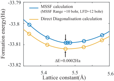
As a further test of the multi-site radii, and to characterise the calculations, the equation of state for bulk silicon was calculated using multisite support functions, and compared to diagonalisation in the primitive PAO basis set, as shown in Fig. 1. The difference in energy at the minimum is less than Ha ( eV), while the lattice constants have the same value, 5.47Å. This confirms the accuracy of our multi-site support function parameters. We used this lattice constant for the NWs in the axial direction.
The generalized gradient approximation (GGA) in the form of the PBE exchange-correlation functional Perdew et al. (1996) was used in all calculations. We note that this choice of functional will result in inaccuracies in the band gap calculated (as seen below in Sec. III.1). Use of a hybrid functional would improve the band gap, though a screened functional might be necessary to account for the extension of the systemJanesko et al. (2009), and it is not always clear what fraction of exchange is needed in a given system. While there might be some changes to the curvature of the bands, the largest effect on the band structure would be to open the gap. While most integrals are performed analytically or radially, we still require a real-space grid for some matrix elements, and we set the integration grid cutoff to 80 Ha, which was identified as sufficient for the DFT total energy to converge within eV. Structural relaxations used a Monkhorst-Pack grid with a density of , where the NW is assumed to lie along the z-axis. The NW was constrained along the [110] axial direction, but is free to expand along the radial direction. The Si NW is put in a unit cell with more than 13 Å vacuum spacing in the transverse directions to avoid any interactions between the neighboring image NWs due to periodicity. The Si NWs are relaxed until the absolute value of force acting any atom is less than 0.02 eV/Å using the FIRE algorithm Bitzek et al. (2006).
III Results and Discussion
III.1 Pure Si NWs
The most frequently reported growth directions for Si NWs are [110] and [111] directions, and less frequently, the [112] directionWu et al. (2004); Ma et al. (2003). Si NWs with diameters in the range of our study primarily grow along the [110] directionWu et al. (2004); Ma et al. (2003), with a hexagonal cross section, bounded by four (111) and two (001) surface facets. Larger diameter NWs are known to grow in [112] and [111] directionsWu et al. (2004), but we will not consider them here.
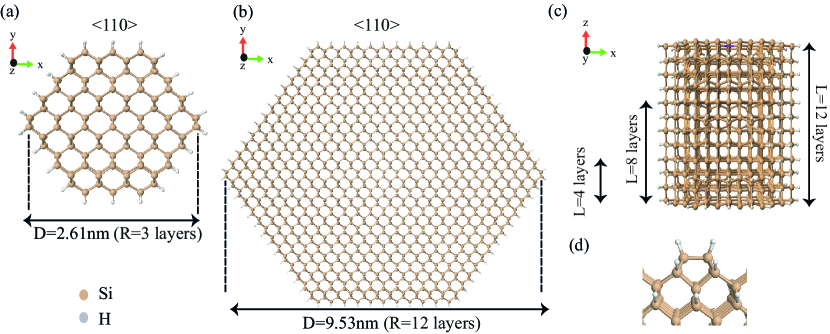
Cross-sectional models of the smallest and largest diameter pure Si NWs considered in this work are shown in Fig. 2(a) and 2(b) respectively. The dangling bonds of Si atoms on the surface are passivated by H, as illustrated in Fig. 2(d); we note that the (001) surface is dimerised, with a monohydride termination. An axial view of the supercell used for the NWs is shown in Fig. 2(c), illustrating the three lengths considered: one (L=4 layers), two (L=8 layers) and three primitive cells (L=12 layers) along the axial direction.
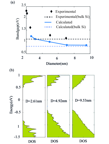
We start by considering the effect of the NW diameter on the electronic structure of pure silicon; for this part of the study, we use only one repeat length along the axis. Figure 3(a) shows the band gap of pure Si NWs of different diameters, ranging from 2.61 nm to 9.53 nm. The sharp increase in the band gap with the reduction of diameter can be attributed to quantum confinement effects. Our calculated values follows the trend seen in the experimental dataMa et al. (2003) very well. For bulk silicon, the experimental band gap at room temperature is 1.12 eV. Experimentally obtained bandgap values converge to this bulk value with increasing diameter. Similar behaviour can be seen in our calculated values, though these are affected by the well-known problem with band gaps in DFT. Our NW gap does converge to the calculated bulk band gap with increasing diameter.
Going into more detail, we also see that the density of states for the full NW is strongly affected by the NW diameter in Fig. 3(b). The smallest diameter NW has a very high variation in electronic states with changing energy, while this variation becomes smoother with the higher diameter NWs (this is in part due to the larger number of atoms included in modelling).
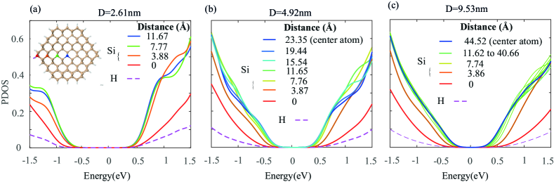
In charge transport related applications, the states near the edges of conduction and valence bands dominate the transport properties. Therefore, it is important to understand which atoms contribute to the edges of the conduction valence bands most. Figure 4 shows partial densities of states projected onto specific atoms at different distances from the surface of the NWs, concentrating on the region around the Fermi level. Due to the difference in strain and surrounding environment experienced by the atoms based on their position, the contribution is not the same. It can be seen that, regardless of the diameter, Si atoms in the two layers closest to the surface contribute least to the band edges, while the atoms at the center of the NW have a higher contribution. When considering the contributions within 0.5 eV of the band edges, it can be noted that the magnitude of the contribution is inversely proportional to the distance from the surface. Moreover, the H atoms used for passivating the dangling bonds have a negligible contribution, when compared with the Si atoms (this is entirely expected if they function purely as passivation). Electronic transport will therefore likely be largely far from the surface of the Si NWs. The Si-Si distance near the surface is slightly more than the Si-Si distance near the centre. The influence from the H atoms in combination with this factor leads to the PDOS behaviour observed. Similar PDOS characteristics have been seen in other NW studiesNg and Tong (2012).
III.2 As-doped Si NWs
We now turn to doping; we study As-doped Si NWs with radii of 3 ,6 and 9 layers (D=2.61, 4.92 and 7.34 nm) with the aim of understanding the the role played by the dopants and its positioning on the electronic band structure. These positions are selected with the intention of identifying different effects when the dopants are close to the surface and away from the surface. We limit the radii compared to the pristine NWs (which extended to 12 layers) so that we can extend the axial size of the NW to isolate the dopants. Our tests showed that the change in radius from 9 to 12 layers gives only very small changes in electronic structure (e.g. the gap in Fig. 3).
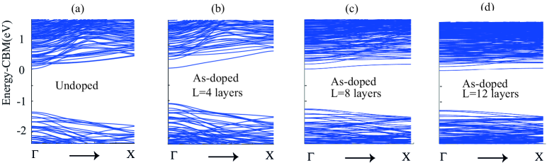
We first test the effect of increasing the axial size of the NW, thus probing the isolation of the dopant along the axis. Figure 5 compares the bandstructures of an undoped NW with doped NWs of different axial lengths (and hence different As doping concentrations). Different doping concentrations were implemented using 1 repeat length (L=4 layers, 0.77 nm), 2 repeat lengths (L=8layers, 1.55 nm) and 3 repeat lengths (L=12 layers, 2.32 nm) in the axial direction of the supercell. The supercell contains a single As atom. The As to Si ratio in each case are 1/159, 1/319 and 1/479 respectively. We have used our smallest diameter NW model which has a radius (R) of 3 layers for these calculations.
As would be expected, the main effect of the introduction of an As dopant is to create a state near the conduction band edge. We can consider the axial length of the NW in terms of dopant concentration, though dopant spacing along the axis (a one dimensional doping concentration) is perhaps a more helpful description. Relatively low levels of doping (L=8 and 12 layers) introduce a rather flat, and hence low velocity, band that leads to a high density of states near the conduction band edge (PDOS for the As atom in the NWs is shown in Fig. 6). The curvature of this band changes with the doping concentration: the flattest band is with L=12 layers, though there is little difference at L=8 layers. At the highest level of doping considered here (L=4 layers), the curvature is significant. Given that this corresponds to a dopant-dopant spacing of 0.77 nm it is reasonable that there is considerable dispersion (in the limit of a strongly delocalised band, we would expect near-parabolic dispersion). The almost flat bands seen for L=8 in Fig. 5(c) and L=12 in Fig. 5(d) suggest that the dopant-dopant interaction is small at a spacing of 1.55 nm and beyond. This fits well with the donor radius for As in bulk silicon, calculated as 1 nmYamamoto et al. (2009); there may be some compression effects on the dopant state from the finite NW radius, but our observation of almost flat bands with a separation of 2.3 nm indicates that they are likely to be small.
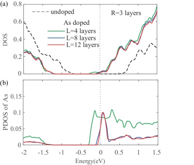
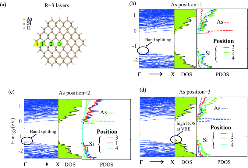
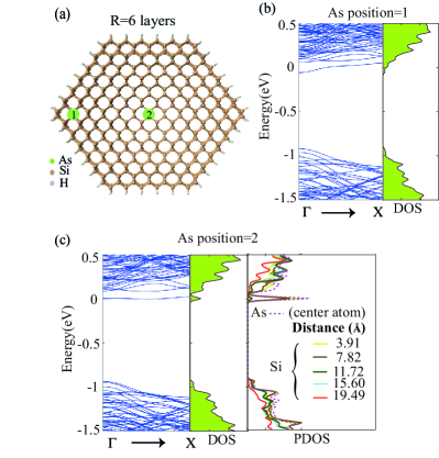
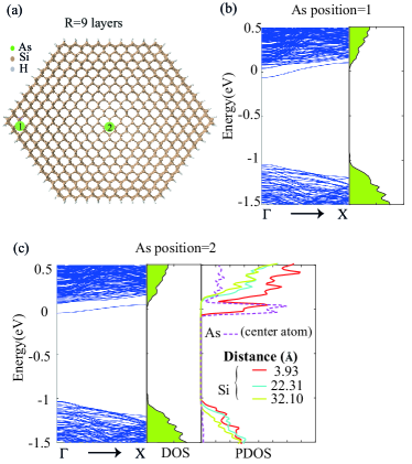
Figure 6(a) compares the total DOS of NWs with different (one dimensional) As doping concentrations. Since As is a n-type dopant, we would expect to observe a defect state near the conduction band, with an accompanying shift in the Fermi level, and this is indeed seen. In addition to this, the defect/dopant band introduced within the bandgap results in increased DOS near the conduction band edge.
For these NWs, the projected DOS of the dopant As atoms is shown in Figure 6(b). The results from two and three repeat lengths are in good agreement with each other. This confirms that at least two repeat lengths in the axial direction are needed to reduce artificial interaction between images of the dopant atoms when simulating Si NWs using DFT methods (we note that previous work modelling boron and phosphorus-doped NWsFernández-Serra et al. (2006); Leão et al. (2008) was confined to much smaller lengths than are used here, mostly L=2 or L=4, though one very small diameter wire with L=10 was modelledLeão et al. (2008)). Accordingly, for the calculations shown in Figs. 7, 8 and 9 we used supercells made of two repeat lengths in the axial direction, i.e L=8, in order to reduce dopant image interaction.
Figure 7 shows the effect of dopant positioning on the density of states, PDOS and the bandstructure, for a NW of R=3 layers. The As atom is placed to substitute a Si atom near the surface (1), in the center (3), or mid-way in between (2). In Fig. 7(b) and (c), it is clear that the valence band edge at the point is split, due to the asymmetry when As is placed in a position other than the center. When the dopant is at the centre of the NW, the band is not split, leading to a higher DOS near the valence band edge. It is also apparent from PDOS that the flat band seen in the bandstructure near the conduction band edge results from the As dopant.
Figure 8 shows similar results as the radius of the NW is increased to R=6 layers. The low velocity dopant band introduced due to doping is slightly further below the conduction band edge than for the R=3 case, and is more significantly affected by the dopant positioning. The centre of the NW is better isolated from the surface in this case, so that the difference to the near-surface location is enhanced. The dopant band becomes flatter and creates strongly localised states near the conduction band edge when the dopant is in the center or close to the center. The PDOS of atoms can be seen for the central dopant placement in Fig. 8(c). The major contributions to the dopant state come from the dopant atom and atoms close to it. Similar to the R=3 layers case, placing the dopant away from the center breaks the symmetry and cause band splitting near the valence band edge at the point.
In Fig. 9 we explore our largest doped NW, with R=9 layers. The super cell containing two unit cells in the axial direction is made up of 2,472 atoms (2,239 Si atoms,1 As atom and 232 H atoms). Similar to the smaller diameter NWs above, a low velocity band is introduce by the doping, and the valence band edge band splitting can be seen when the dopant is placed in an asymmetric position. The overall DOS in Fig. 9(b) is much smoother, and the dopant state does not appear very prominent, due to the large number of atoms in the system. The PDOS in Fig. 9(c) still show the dopant state clearly, with contributions from neighbouring silicon atoms.
IV Conclusion
In conclusion, we have used the Conquest local orbital DFT code to study both pure and doped Si NWs with diameters up to 9.53 nm and 7.34 nm respectively. For the undoped NWs, the bandgap reduces with increasing diameter and converges to its bulk value, which is in agreement with experimental data. The atoms closest to the surface of the NW contributes less to the states near the band edges, when compared with atoms close to the centre. This is due to differences in Si-Si atomic distances and surface passivation effects.
When considering As-doped Si NWs, the dopant placement is important, because it effects electronic structure and hence important properties such as electronic transport. A low velocity band in the gap is introduced by As doping, close to the conduction band edge. The dopant positioning affects the curvature of this band. The curvature reduces when the dopant is placed closer to the center, creating strong peaks in the density of states. Asymmetric placement of the dopant creates band splitting in the valence band edge which is visible quite prominently in the DOS of low radii NWs. This study demonstrates the importance and utility of large-scale density functional approaches such as those used in Conquest. It is important to note that significantly larger calculations are possible using multi-site support functions with exact diagonalisation (up to 10,000 atoms), while linear scaling calculations are feasible on 100,000+ atoms, with techniques available to recover electronic structure near the Fermi levelNakata et al. (2017). These approaches show great promise in the study of experimentally relevant NWs.
Acknowledgements.
The authors are grateful for computational support from the UK Materials and Molecular Modelling Hub, which is partially funded by EPSRC (EP/P020194), for which access was obtained via the UKCP consortium and funded by EPSRC grant ref EP/P022561/1.References
- Peng and Lee (2011) K.-Q. Peng and S.-T. Lee, Advanced Materials 23, 198 (2011).
- Tsakalakos et al. (2007) L. Tsakalakos, J. Balch, J. Fronheiser, B. Korevaar, O. Sulima, and J. Rand, Applied Physics Letters 91, 233117 (2007).
- Hochbaum et al. (2008) A. I. Hochbaum, R. Chen, R. D. Delgado, W. Liang, E. C. Garnett, M. Najarian, A. Majumdar, and P. Yang, Nature 451, 163 (2008).
- Boukai et al. (2008) A. I. Boukai, Y. Bunimovich, J. Tahir-Kheli, J.-K. Yu, W. A. Goddard Iii, and J. R. Heath, Nature 451, 168 (2008).
- Miao et al. (2014) R. Miao, L. Mu, H. Zhang, G. She, B. Zhou, H. Xu, P. Wang, and W. Shi, Nano letters 14, 3124 (2014).
- Cui et al. (2001a) Y. Cui, Q. Wei, H. Park, and C. M. Lieber, Science 293, 1289 (2001a).
- Jee et al. (2014) S.-W. Jee, K. Zhou, D.-W. Kim, and J.-H. Lee, Nano Convergence 1, 29 (2014).
- Cui and Lieber (2001) Y. Cui and C. M. Lieber, science 291, 851 (2001).
- Koo et al. (2005) S.-M. Koo, Q. Li, M. D. Edelstein, C. A. Richter, and E. M. Vogel, Nano letters 5, 2519 (2005).
- Cui et al. (2001b) Y. Cui, L. J. Lauhon, M. S. Gudiksen, J. Wang, and C. M. Lieber, Applied Physics Letters 78, 2214 (2001b).
- Morales and Lieber (1998) A. M. Morales and C. M. Lieber, Science 279, 208 (1998).
- Lew et al. (2004) K.-K. Lew, L. Pan, T. E. Bogart, S. M. Dilts, E. C. Dickey, J. M. Redwing, Y. Wang, M. Cabassi, T. S. Mayer, and S. W. Novak, Applied Physics Letters 85, 3101 (2004).
- Cui et al. (2000) Y. Cui, X. Duan, J. Hu, and C. M. Lieber, The Journal of Physical Chemistry B 104, 5213 (2000).
- Ma et al. (2001) D. Ma, C. Lee, and S. Lee, Applied Physics Letters 79, 2468 (2001).
- Colinge et al. (2010) J.-P. Colinge, C.-W. Lee, A. Afzalian, N. D. Akhavan, R. Yan, I. Ferain, P. Razavi, B. O’neill, A. Blake, M. White, et al., Nature nanotechnology 5, 225 (2010).
- Tang et al. (2005) Q. Tang, T. I. Kamins, X. Liu, D. Grupp, and J. S. Harris, Electrochemical and Solid-State Letters 8, G204 (2005).
- Ng et al. (2011) M.-F. Ng, M. B. Sullivan, S. W. Tong, and P. Wu, Nano letters 11, 4794 (2011).
- Zhao et al. (2004) X. Zhao, C. Wei, L. Yang, and M. Chou, Physical review letters 92, 236805 (2004).
- Ng and Tong (2012) M.-F. Ng and S. W. Tong, Nano letters 12, 6133 (2012).
- Zhuo and Chou (2013) K. Zhuo and M.-Y. Chou, Journal of Physics: Condensed Matter 25, 145501 (2013).
- Leu et al. (2008) P. W. Leu, A. Svizhenko, and K. Cho, Physical Review B 77, 235305 (2008).
- Peelaers et al. (2006) H. Peelaers, B. Partoens, and F. M. Peeters, Nano letters 6, 2781 (2006).
- Leão et al. (2008) C. R. Leão, A. Fazzio, and A. J. da Silva, Nano letters 8, 1866 (2008).
- Fernández-Serra et al. (2006) M. Fernández-Serra, C. Adessi, and X. Blase, Physical review letters 96, 166805 (2006).
- O’Rourke et al. (2018) C. O’Rourke, S. Y. Mujahed, C. Kumarasinghe, T. Miyazaki, and D. R. Bowler, J. Phys.: Condens. Matter 30, 465303 (2018).
- Bowler et al. (2002) D. Bowler, T. Miyazaki, and M. Gillan, Journal of Physics: Condensed Matter 14, 2781 (2002).
- Bowler and Miyazaki (2010) D. R. Bowler and T. Miyazaki, Journal of Physics: Condensed Matter 22, 074207 (2010).
- Ma et al. (2003) D. Ma, C. Lee, F. Au, S. Tong, and S. Lee, Science 299, 1874 (2003).
- Wu et al. (2004) Y. Wu, Y. Cui, L. Huynh, C. J. Barrelet, D. C. Bell, and C. M. Lieber, Nano letters 4, 433 (2004).
- Wang et al. (1999) N. Wang, Y. Tang, Y. Zhang, C. Lee, I. Bello, and S. Lee, Chemical physics letters 299, 237 (1999).
- Sivakov et al. (2010) V. A. Sivakov, F. Voigt, A. Berger, G. Bauer, and S. H. Christiansen, Physical Review B 82, 125446 (2010).
- Selberherr (2012) S. Selberherr, Analysis and simulation of semiconductor devices (Springer Science & Business Media, 2012).
- Reenu et al. (2015) R. Reenu, G. S. Devi, and M. Rajendran, International Journal of ChemTech Research 8, 1846 (2015).
- Bowler and Miyazaki (2012) D. R. Bowler and T. Miyazaki, Reports on Progress in Physics 75, 036503 (2012).
- Nakata et al. (2014) A. Nakata, D. R. Bowler, and T. Miyazaki, Journal of chemical theory and computation 10, 4813 (2014).
- Torralba et al. (2008) A. S. Torralba, M. Todorovic, V. Brázdová, R. Choudhury, T. Miyazaki, M. J. Gillan, and D. R. Bowler, J. Phys. Condens. Matter 20, 294206 (8pp) (2008).
- Nakata et al. (2015) A. Nakata, D. Bowler, and T. Miyazaki, Phys. Chem. Chem. Phys. 17, 31427 (2015).
- Rayson and Briddon (2009) M. Rayson and P. Briddon, Physical Review B 80, 205104 (2009).
- Rayson (2010) M. Rayson, Computer Physics Communications 181, 1051 (2010).
- Perdew et al. (1996) J. P. Perdew, K. Burke, and M. Ernzerhof, Physical review letters 77, 3865 (1996).
- Janesko et al. (2009) B. G. Janesko, T. M. Henderson, and G. E. Scuseria, Phys. Chem. Chem. Phys. 11, 443 (2009).
- Bitzek et al. (2006) E. Bitzek, P. Koskinen, F. Gähler, M. Moseler, and P. Gumbsch, Physical review letters 97, 170201 (2006).
- Yamamoto et al. (2009) T. Yamamoto, T. Uda, T. Yamasaki, and T. Ohno, Physics Letters A 373, 3989 (2009).
- Nakata et al. (2017) A. Nakata, Y. Futamura, T. Sakurai, D. R. Bowler, and T. Miyazaki, J. Chem. Theor. Comput. 13, 4146 (2017).