]Contributed equally. ]Contributed equally.
Segmented ion-trap fabrication using high precision stacked wafers
Abstract
We describe the use of laser-enhanced etching of fused silica in order to build multi-layer ion traps. This technique offers high precision of both machining and alignment of adjacent wafers. As examples of designs taking advantage of this possibility, we describe traps for realizing two key elements of scaling trapped ion systems. The first is a trap for a cavity-QED interface between single ions and photons, in which the fabrication allows shapes that provide good electro-static shielding of the ion from charge build-up on the mirror surfaces. The second incorporates two X-junctions allowing two-dimensional shuttling of ions. Here we are able to investigate designs which explore a trade-off between pseudo-potential barriers and confinement at the junction center. In both cases we illustrate the design constraints arising from the fabrication.
I INTRODUCTION
Atomic ions trapped in radio frequency traps cooled and controlled by laser light provide an experimental platform which is extremely well isolated from environmental effects. As a result, this setting is among the leading candidates for quantum computing Bruzewicz et al. (2019); Brown et al. (2011); Harty et al. (2014); Benhelm et al. (2008); Ballance et al. (2016) as well as playing an important role in precision measurements and frequency standards Kozlov et al. (2018); Gebert et al. (2015); R. Leibrandt et al. (2017). In both areas extending the current levels of control to larger numbers of ions is important. This is obvious for a quantum computer, which will rely on manipulating a large number of qubits. For atomic clocks an increase in the number of ions under control would provide improved signal-to-noise ratio Herschbach et al. (2012), while including techniques known from quantum computing could further enhance this through the use of entanglement Blatt and Wineland (2008).
One challenge of putting together systems with more ions is the realization of suitable trap structures which can be easily and repeatably fabricated. These must meet a number of requirements, including having precise and uniform structures, allowing good optical access, and being able to withstand the high voltages and resulting electric fields (including radio-frequency fields) which are commonly used. As these systems become more extensive, the alignment of the electrode structures becomes increasingly important Pyka et al. (2014). In quantum computing, particular challenges arise for trap development in the context of the “Quantum CCD” architecture, in which ions are dynamically shuttled through multiple connected zones of a trap array during the execution of algorithms Kielpinski et al. (2002); Blakestad et al. (2009). For scaling it may also be necessary to interface the ion with photonic connections between remote modules. Two elements which are integral to these approaches are junction regions which can guide ions in two dimensions, and single-ion/single-photon interfaces. In the long term scaling may also require the integration of a variety of components into the trap structure, such as optics for light delivery and collection M. Eltony et al. (2012); Van Rynbach et al. (2016).
A number of approaches have been taken previously in an attempt to realize suitable traps using techniques which can potentially be scaled to larger systems while maintaining precision. Common requirements are that electrode structures of a few 100 micron size can be realized, while retaining a precision of the electrode boundaries at close to 1 micron. One important area of research involves traps which are produced by lithography Doret et al. (2012); Seidelin et al. (2006); Pearson et al. (2005), which allows the production of monolithic structures which are very precisely defined (at the level of a few 10s of nanometers). However it is difficult in many of these processes to fabricate multi-layer stacks to thicknesses of more than a few tens of microns Stick et al. (2006). The heating of ions near conducting surfaces decreases rapidly with distance, thus ion-electrode distances used for experiments have all been m, which is greater than the lithographic thickness. Because of this most lithographic traps have been surface-electrode traps, in which the ions are trapped above a single plane of electrodes, providing a strong asymmetry in the out-of-plane potential. This configuration results in a sacrifice of trap depth and curvature for fixed ion-electrode distance and voltage compared to more symmetric electrode designs. This makes tasks such as shuttling through two-dimensional junctions more challenging Blakestad et al. (2009); Wright et al. (2013).
Micro-fabricated ion traps with heights of 100 micron or more have been produced using either stacks of wafers which are aligned manually Kienzler (2015); Blakestad (2010), or in a monolithic fashion using silicon fabrication techniques developed for Micro-Electrical-Mechanical-Systems (MEMS) Brownnutt et al. (2006); Wilpers et al. (2012). Wafer stacking techniques have generally relied on combinations of optical monitoring and manual alignment, which is limited to tens of microns. Several experiments using stacked laser-machined alumina wafers have reported suspected misalignment as a cause of undesirable intrinsic micromotion Gaebler et al. (2016); Negnevitsky (2018). This reduces the interaction strength between an ion and a single-frequency laser beam, thus impeding control, and gives rise to an important systematic shift in frequency standards HerschbachK et al. (2012). The monolithic approach potentially overcomes this problem Brownnutt et al. (2006); Wilpers et al. (2012), but these traps have not become reliably available to experimentalists and thus are relatively unexplored.
In this article, we describe the use of laser-enhanced etching to construct precisely machined 3-dimensional ion traps based on stacked fused silica wafers. We use the precision and flexibility of this manufacturing method to design self aligning stackable structures, detail the capabilities and constraints of this approach, and give guidance in designing traps. We present two trap designs for quantum computing experiments which take advantage of these methods. The first is a segmented linear trap for which the electrode structures are designed to provide a high level of electro-static shielding of the ion from potential charge build up on an externally mounted optical cavity. The second is a segmented trap featuring two junctions, which should allow flexible re-configuration of arrays of ions. We give the results of testing the wafer alignment, as well as detailing the full fabrication chain that we have developed.
II Femtosecond laser-enhanced etching
Femtosecond laser-enhanced etching consists of exposing a glass substrate to femtosecond laser light followed by wet-etching with a dilute hydrofluoric acid solution Marcinkevičius et al. (2001). It has been observed that silica exposed to femtosecond laser light has a significantly faster etching rate compared to not exposed silica Kondo et al. (1998); Marcinkevičius et al. (2001). This is believed to be due to the creation of an internal stress field and a change in the chemical structure of the silica Bellouard et al. (2004). Due to the non-linear nature of femtosecond laser interaction with silica, enhancement of the etching rate occurs only in a small ellipsoidal volume in the focus of the beam referred to as the Laser Activated Zone (LAZ) Bellouard et al. (2003), shown in Figure 1. Thus, the full volume to be etched needs to be written into the substrate by the laser. It has also been observed that in volumes with multiple laser exposures the etching rate is even higher than in domains that have been exposed only once Bellouard et al. (2004).
In recent years several experiments and applications have demonstrated the strength of this technology. Applications include laser written optical waveguides Bellouard et al. (2003); Davis et al. (1996); Streltsov and Borrelli (2002); Hirao and Miura (1998); Miura et al. (1997), creation of high aspect ratio micro-fluidic channels Bellouard et al. (2004, 2003); Bellouard (2011), flextures Bellouard (2011), MEMS Lenssen and Bellouard (2012) and ion traps Yoshimura et al. (2015); An et al. (2018); Dugan et al. (2015). We are currently aware of two companies offering a customizable femtosecond laser machining service: Translume https://translume.com (2018) in the United States, and FEMTOprint https://www.femtoprint.ch (2018); et al. (2012) in Switzerland. The work below has been carried out with devices fabricated by the latter.
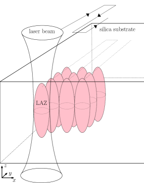
II.1 Capabilities of the machining process
In the following sections we will discuss the strengths and main limitations of femtosecond laser machining of silica with regard to ion trap fabrication. We focus on the achievable tolerances stated by FEMTOprint and give an overview of our own experiences with test devices designed while working with FEMTOprint’s team. We focus on the machining precision, the achievable aspect-ratio of 3-dimensional structures such as grooves and cuts and the ability to create small yet precisely defined 3-dimensional geometries.
As a result of the shape of the LAZ, the specified process precision of femtosecond laser-enhanced etching is in the direction of propagation of the laser beam (hereafter these will be referred to as horizontal surfaces, with the laser beam assumed to propagate vertically) and https://www.femtoprint.ch (2018) orthogonal to it (these surfaces we refer to as vertical). On our test samples we have observed that these values represent a “best case scenario”, which can be achieved in localized regions. In larger structures and over full wafers we observe machining tolerances on the 10 micron level.
![]()
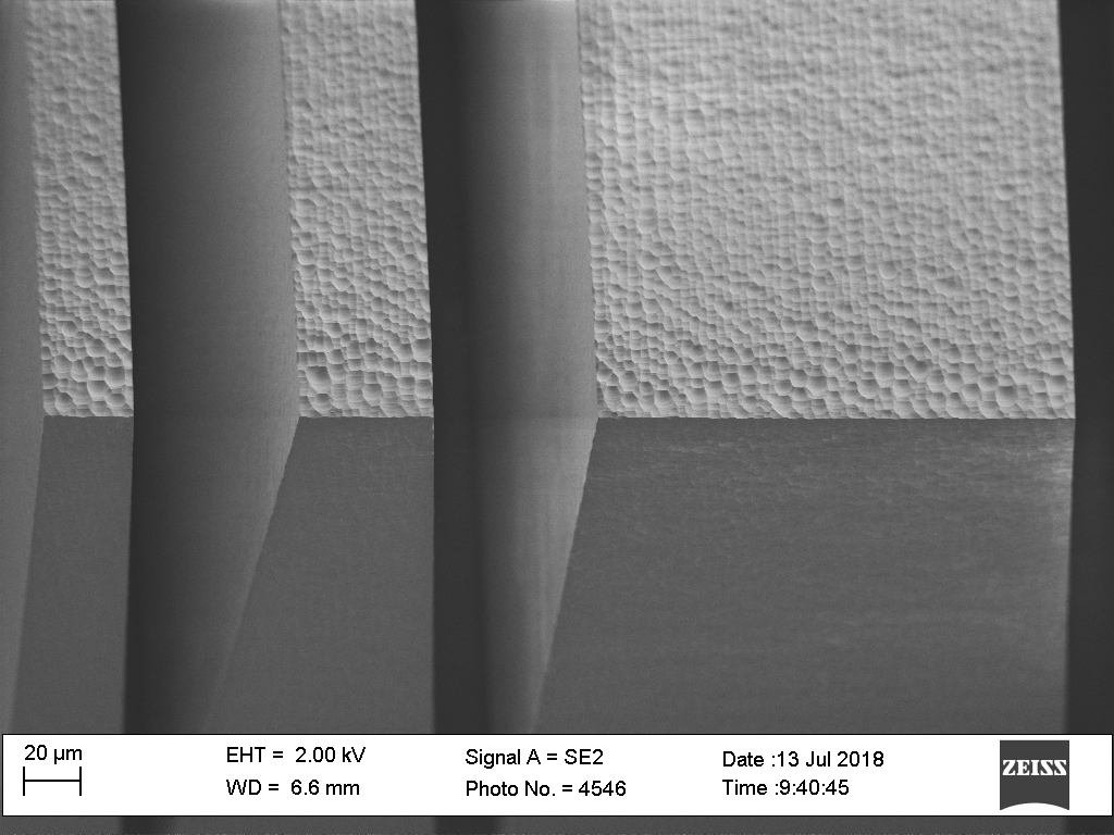
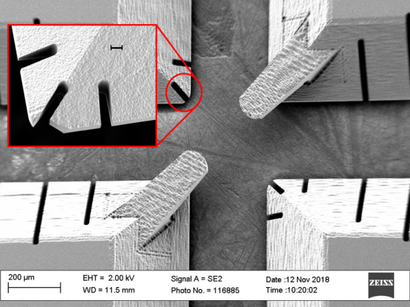
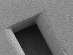
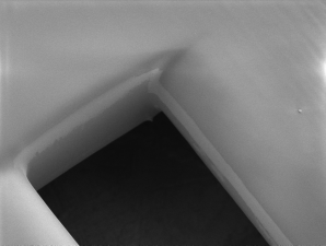
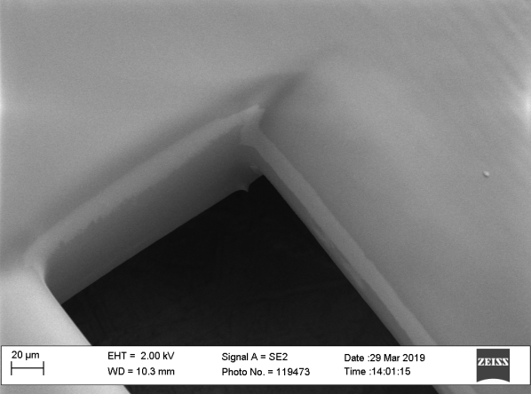
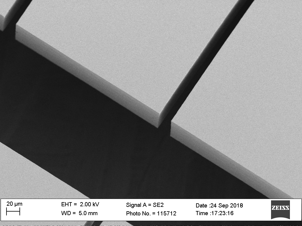
The aspect ratio we tested for cuts and grooves was up to 1:50, which is sufficient for our applications, although the manufacturer quotes an achievable aspect ratio of up to 1:500 https://www.femtoprint.ch (2018). Our test samples have shown that cuts feature very regular and sharp edges (Figure 2 a.)). From SEM images we estimate the radii of curvature of the edges to be less than 100 nm. We also observe that the femtosecond laser enhanced etching is capable of forming 3D shapes with sizes as small as 10 including freely protruding structures such as those shown in 2 b.). The laser-enhanced etching process is automized https://www.femtoprint.ch (2018), which in our experience results in short turnaround times on the order of a few weeks and thus provides the possibility for relatively fast prototyping.
II.2 Limitations of the machining process
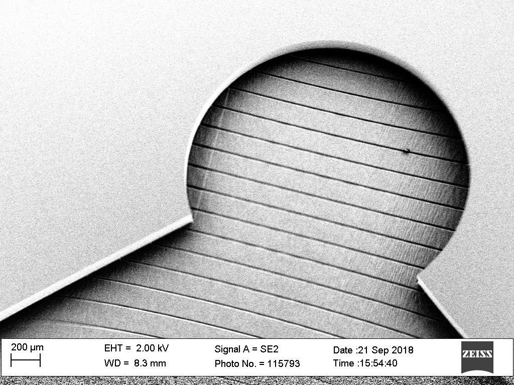
While the versality of the laser-enhanced etching process is attractive, it is important to consider a number of factors which lead to imperfections. The first is that due to the shape of the LAZ and the nature of volume sampling the surface quality differs on horizontal and vertical surfaces. Panel a.) of Figure 2 shows the top side of a sampled volume (surfaces perpendicular to the laser beam), for which the etching leads to a characteristic surface roughness on the order of hundreds of nanometers. Also shown are the sides where the surface roughness is only on the order of a few tens of nanometers. Surfaces with high roughness can be smoothened using an additional polishing step in which the femtosecond laser is re-used to melt the surface of the machined structure. Due to surface tension the surface becomes very smooth with micro roughness on the order 1 nm and a flatness that is still on the order of 10 - 100 nm. The result of polishing is shown in panel c.) of Figure 2. However, besides the desired smoothing of surfaces, structures such as edges and steps are also softened by this thermal polishing step.
A second challenge arises when large quantities of substrate material are removed. During intense laser irradiation local heating can occur in the silica, which can lead to a slight bending or expansion of the sample during laser writing. As a consequence the overall process quality and precision is reduced. The removal of large quantities of material can also create stress in the sample. We have observed that this can result in small defects with sizes on the order of 10 to 20 m. When working with 125 m thick wafers we observed regular grooves on horizontal surfaces after etching, which did not occur with thicker wafers of similar material. Defects as well as grooves are especially likely to occur at positions where a large fraction of the surrounding material has been removed. Examples thereof from our junction trap are shown in Figure 2 b.) and d.) and the inset of 2 b.). If these defects can not be tolerated, they limit the process yield since the occurrence is unpredictable. The removal of large quantities of material also requires a long laser irradiation step, which increases the process cost.
III Multi-layer trap design concept
We use the femtosecond laser-enhanced etching to develop ion trap wafers that offer simple and high precision wafer-to-wafer alignment. Our alignment strategy utilizes the precision machining to realize a three point support mechanism with the relevant alignment features directly machined into the individual wafers. These then self-align when placed on top of each other. In the following we describe this alignment scheme and establish general guidelines for the design of similar traps.
III.1 Alignment strategy
Our alignment scheme is based on a three point support mechanism, which mechanically defines the relative orientation of neighbouring wafers. In the two traps described below, we have used a stack of three wafers, with the middle wafer defining the three support points for the other two. Any of these wafers might be used for electrodes. In our assembly process the wafers are placed together with a small amount of clamping force, and then glued in place.
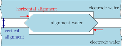
The design of the alignment points is illustrated in the cross-section sketch in 3 a.). We found that the alignment points on the middle wafer work well if they are half circles with chamfer on the top and bottom side each half way through the wafer. A first approach with fully integrated alignment features failed due to poor precision and low surface quality (see appendix A).
The respective counterpart for the alignment on the outer wafers is an indentation (see Figure 4 a.)). The walls of the indentation are vertical and make a right angle with the top surface of the wafer. The size (and shape) of the inset is designed such that electrode and alignment wafers only touch each other at the alignment points. With the high precision attained by the machining, we achieve stable and precise alignment of the three wafers.
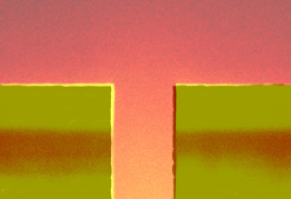
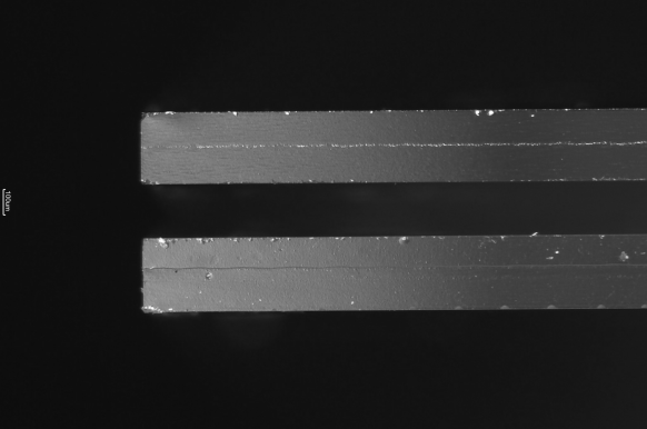
Figure 3 b.) shows a measurement of the relative alignment of two wafers which are separated by an intermediate spacer in the manner described. The measurement is carried out using an optical microscope equipped with a CCD-camera. First the microscope is focused on an electrode of the bottom wafer of the wafer-stack and a picture is taken. Next, the microscope is focused on the same electrode on the top wafer and another picture is taken. Then the two pictures are overlapped pixel by pixel (both with increased contrast and one with inverted colors to obtain bright areas appearing dark). From the known pixel size and microscope magnification we can estimate the misalignment between the wafers. The measurement is limited by the depth of view and precision of mechanical parts of the microscope that could shift the images during refocusing. Nevertheless it allows us to constrain the relative alignment imprecision to m. The stated alignment precision is for wafers of dimension of . Similar measurement results were obtained at different points distributed over the full trap.
A measurement of the vertical alignment is shown in panel c.) of Figure 3. We have observed that vertically the angle between the wafers is less than 0.05 deg while the separation relies on the thickness tolerance of the substrates. This typically lies between and . By measuring the thickness of the alignment wafer prior to fabrication, the alignment feature on the electrode wafers could be adjusted to compensate for thickness deviation and thus the vertical alignment of the wafers could be improved if desired. Within individual wafers, we have measured a homogeneous flatness over the full area of mm within uncertainty () of the instrument. Even when wafer flatness varies by a few microns over the whole area, placing the alignment points far from each other ensures only a small variance in the angle between electrodes on each wafer.
III.2 Wafer and electrode design
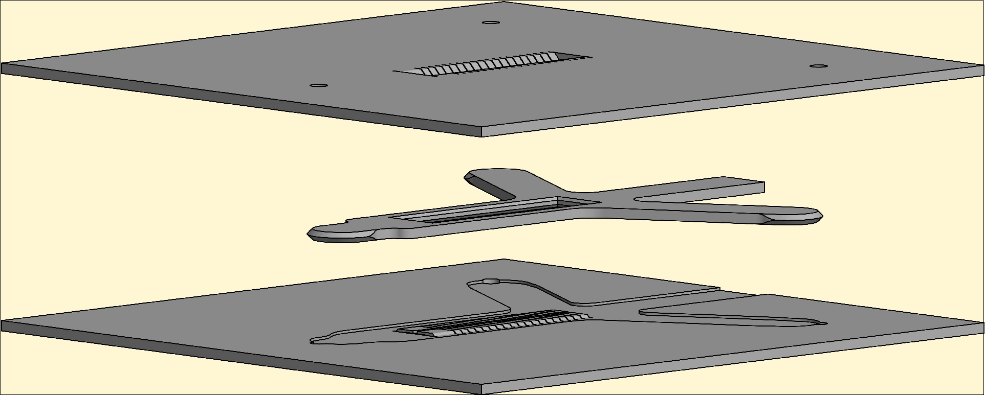
One possible wafer design is illustrated in Figure 4 a.) and b.). For this design the trap is positioned in the center of the wafers between the three alignment points. The middle wafer features a slot in the center where the trap is located. Furthermore, the shape of the middle wafer allows the electrodes defined on the top and bottom wafer to extend towards the trap center (see Figure 4 b.) and 6 a.)). In this way, the electrodes are defined on a non-machined surface and vertical cuts through the wafer define the trap area and segmentation of the electrodes. An example of machined electrodes is shown in Figure 4 c.). The silica electrodes show sharp regular edges and very little surface roughness on the vertical faces of the segments, which is beneficial for building a small trap with low ion-electrode distance.
A judicious choice of initial wafer thickness is advantageous, since it prevents adverse effects associated with the removal of a large amount of material.

IV Specific trap designs
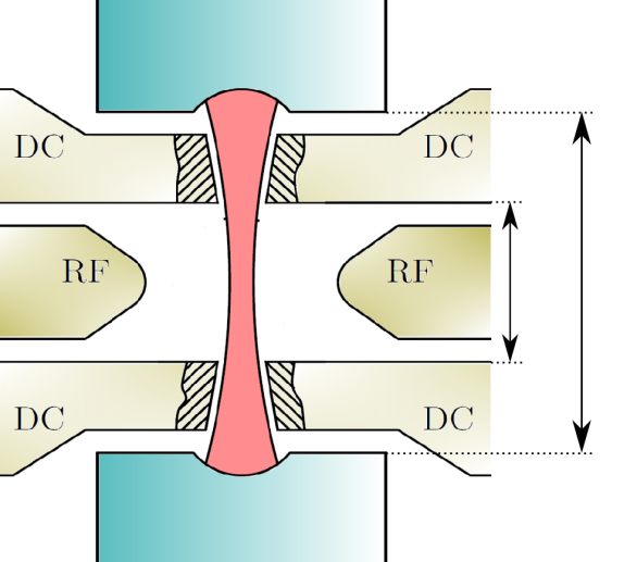
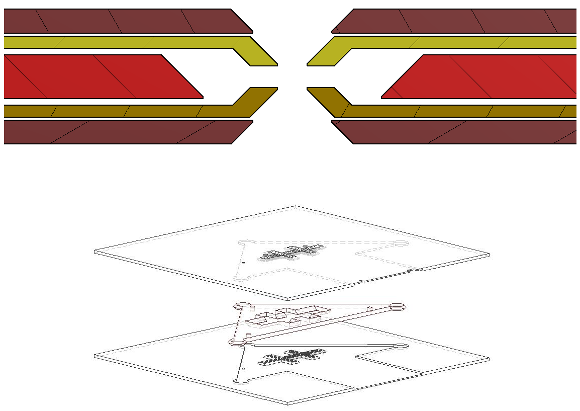
In this section we present two trap designs which aim to investigate aspects of scaling trapped-ion control for quantum information processing. The first trap design is a linear segmented trap which was designed to be compatible with a short-length optical cavity for enhanced ion-photon coupling Takahashi et al. (2018). One primary concern in designing a trap integrated with an optical cavity is that the dielectric coatings of the mirrors can accumulate stray charges which disturb the ions Harlander et al. (2010). Thus, shielding of stray fields is highly desirable. The machining precision provided by the laser-assisted etching described above allows to build a small multi-layer trap, in which electrodes can be placed in-between the cavity mirrors while keeping the cavity length short - in this case we aim for a cavity of length 300 m. A cross-section illustration of the proposed cavity region is shown in Figure 6 a.). The trap design is based on three layers; two layers with DC-electrodes and one with RF-electrodes which is sandwiched between the other two, also serving as alignment wafer.
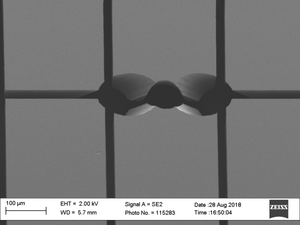
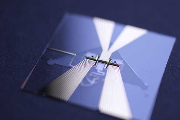
In our trap prototype we aim for an ion to nearest electrode distance of around . Access for laser beams and the cavity mode is provided through holes with diameter in the electrodes, which otherwise block all optical access. This provides shielding against stray fields originating outside the electrode structure. A close up view of these holes is shown in Figure 6 b.). The trap features two regions suited for optical cavities or optical fibers for light collection and delivery. It also includes an open “loading” region so that an atomic beam can be introduced for loading ions. A view of the DC electrodes over the full length of the trap is shown in Figure 6 d.). The ions will be shuttled along the trap axis using the segmented electrodes.
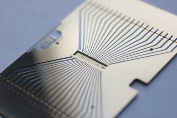
The second trap we have designed and fabricated is a 3-dimensional segmented double junction trap. The trap consists of a total stack of 5 wafers, as shown in Figure 6c.): a middle wafer which serves as a spacer and alignment piece, two outer wafers which carry the main DC and RF trapping electrodes, and two additional wafers carrying electrodes for stray field compensation. The three central wafers, which are the inner ones in the full stack, are shown in Figure 6 e.). All wafers are self aligned in a similar fashion as described in section III A, and subsequently glued to each other. This trap has 144 electrodes, and includes many independently addressable experimental zones as well as splitting, junction and storage zones. The two X junctions are key ingredients for ion transport into 2-dimensions, which is critical for scaling. Several features rely on the ability to form 3-dimensional structures in fused silica. One such feature is the RF electrode shape at the junction. Other features which we have implemented are electrodes angled at 45 degrees and vias for electrode connectivity. In initial designs we also included deep grooves which could host integrated optical fibres. We will briefly describe each in the following.
At the corners of the electrodes at the junction, two opposing protrusions (Figure 7 a.) and b.)) are used to break the symmetry of electric fields, producing 3-dimensional confinement of an ion at the center of the junction, which is not present for a 4-fold symmetric design Blakestad (2010). A previous junction trap was built at NIST, but featured full bridges which crossed from one side of the junction to the other Blakestad (2010). Both the protrusions and bridges give rise to pseudopotential energy barriers which the ion must traverse as it enters the junction. However these are much larger for a full bridge than for the protrusions.

Gradients of the pseudopotential at the sides of the barriers can introduce undesirable heating mechanisms. With the flexibility available from the laser-enhanced etching, we are able to chose the length of the protrusions - the final design was chosen as a compromise between confinement at the center and the magnitude of the energy barriers. The resulting protrusions are 100 m wide and 50 m thick.
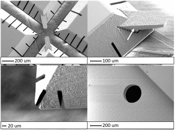
The front surface of all electrodes is angled at 45 degrees to provide high optical access for laser beams and a large solid angle for light collection. Since these faces are machined they exhibit a roughness of hundreds of nm, as visible in Figure 7 c.). This roughness is not on the side of the trap that faces the ion, therefore any imperfections on this face should be shielded at some level from the ion. The RF electrode is defined on the inner (ion-facing) side of the wafer, and then is connected through a via (Figure 7 d.)) to the top wafer surface where it is wire bonded. The via consists of a 0.3 mm diameter hole with vertical faces. The electrical connection is made by evaporating gold on it at an angle. We have investigated the resistance of the electrode when evaporated with a thin layer of gold (700 nm) and have detected an increase of the resistance through the via on the order of 1 Ohm. Typically, evaporated tracks in the range of 10 mm in length (as are often used in electrode connections) exhibit a resistance between 1 and 5 Ohms. A subsequent electroplating step should allow to further reduce this resistance. Different via diameters are also possible. Tests on a 300 m thick wafer have shown that holes can be machined reliably down to a 50 m diameter. As we can fully coat gaps with width on the order of 20 m and similar vertical depth, we think that it should be possible to fully coat 50 m vias.
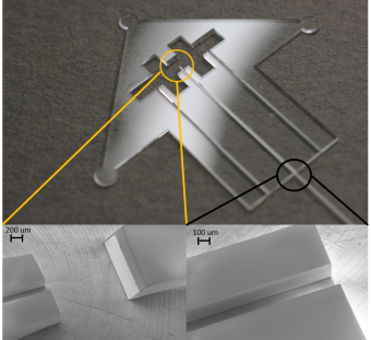
A further set of tests were performed to assess the viability of incorporating optical fibres for laser beam delivery. For this purpose, following the approach of Ott (2016), we fabricated squared grooves into the middle wafer which are shown in inset b.) of Figure 8. We found that these could be machined with horizontal widths which are uncertain to 5 m. Our original aim in these tests was to insert photonic crystal optical fibres (PCF) in these low tolerance grooves, ensuring good vertical and horizontal alignment of the beams. PC fibres were stripped of their coating layer and their glass cladding, which has a 230 5 m diameter, and were inserted and glued in 237 m wide grooves. For laser waist diameters between 30 and 40 m, this technique provides a relatively easy and robust alignment, with maximal theoretical displacements of 6.5 m between the ion’s location and the center of the beam waist. The PC fibres used had lenses melted onto the tip https://www.wttechnology.com/ (2018), with a working distance in the order of 500 m at 729 nm. To allow light to exit the structure, we envisioned using polished mirror surfaces on the opposite side as the fibre grooves, directing incident light out of the trap structure, as shown in inset a.) of Figure 8. We have used an SEM to image the mirror surfaces machined using laser-enhanced etching, which, when gold coated, seem suitable for our purpose. Their micro-roughness is in the order of a nanometer, as shown in Figure 2 c.).
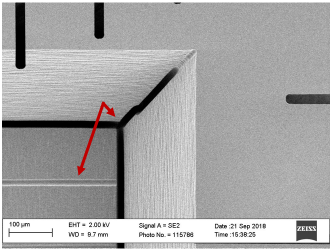
The complex geometries present in the double junction trap produce unexpected stress in the silica substrate. As a consequence we have noticed an increased number of defects, particularly at the junction, where lots of material has been exposed to the laser. We have also observed stray machining cuts on several samples at the interface between different zones of the wafer, such as along the 45 degree angled faces, as shown in Figure 9, and on planar surfaces where material had been removed. These undesired grooves, which can reach 15 m in depth, have been avoided by implementing a small radius of curvature at all intersecting surfaces and by applying a final polishing step following the machining. We conclude that it is important to consider these effects in the design stage.
V Fabrication process
Once the substrates have been fabricated using laser enhanced etching, we use five standard steps to pattern electrodes and wires. All these steps are carried out in a cleanroom environment. The first step is a thorough cleaning of the wafers in a Piranha acid solution. Next the wafers are coated using electron beam evaporation. We apply a titanium adhesion layer with thicknesses on the order of 100 nm, followed by 200 nm of gold. For each wafer, we perform several evaporation steps at different angles to ensure that all desired faces are covered and use laser-cut molybdenum shadow masks to define our electrode tracks. The evaporation is reliable and produces smooth surfaces. Photographs of single wafers from each of the two designs described above are shown in Figure 10. If desired, the evaporation step is followed by electroplating, which thickens the gold layer from a few hundred nanometers to a few microns. Once all trap wafers are coated, we proceed to assemble and to glue them. For the gluing we have used the UV-cured Epotek OG198-55 for traps which we aim to use at room-temperature, and Stycast for traps designed for cryogenic set-ups.
VI Conclusions
We have described how laser-enhanced etching can be used to create precisely aligned multi-wafer stacks with novel features for 3-dimensional ion traps. We outlined a number of possibilities which we have investigated utilizing these techniques. We show that mechanical self-alignment structures are capable of producing alignment tolerances of below 2 m. Based on our experience we think that these fabrication methods are well suited for small-scale multi-wafer and monolithic compact trap designs which could be used in a number of areas, from quantum information processing to frequency standards and precision metrology.
VII Acknowledgments
We thank Andrea Lovera at Femtoprint for many useful discussions, and Matt Grau for comments on the manuscript. We acknowledge funding from the Swiss National Fund under grant numbers and , and from the EU Quantum Flagship H2020-FETFLAG-2018-03 under Grant Agreement no. 820495 AQTION.
References
- Bruzewicz et al. (2019) C. D. Bruzewicz, J. Chiaverini, R. McConnell, and J. M. Sage, Applied Physics Reviews 6, 021314 (2019).
- Brown et al. (2011) K. Brown, A. Wilson, Y. Colombe, C. Ospelkaus, A. Meier, E. Knill, D. Leibfried, and D. Wineland, Physical Review A 84, 030303 (2011).
- Harty et al. (2014) T. Harty, D. Allcock, C. Ballance, L. Guidoni, H. Janacek, N. Linke, D. Stacey, and D. Lucas, Physical Review Letters 113, 220501 (2014).
- Benhelm et al. (2008) J. Benhelm, G. Kirchmair, C. F. Roos, and R. Blatt, Nature Physics 4, 463 (2008).
- Ballance et al. (2016) C. J. Ballance, T. P. Harty, N. M. Linke, M. A. Sepiol, and D. M. Lucas, Phys. Rev. Lett. 117, 060504 (2016).
- Kozlov et al. (2018) M. Kozlov, M. S. Safronova, J. Crespo Lopez-Urrutia, and P. O. Schmidt, Reviews of Modern Physics 90 (2018).
- Gebert et al. (2015) F. Gebert, Y. Wan, F. Wolf, C. N. Angstmann, J. C. Berengut, and P. O. Schmidt, Phys. Rev. Lett. 115, 053003 (2015).
- R. Leibrandt et al. (2017) D. R. Leibrandt, S. M. Brewer, J.-S. Chen, C.-W. Chou, A. M. Hankin, D. B. Hume, and D. J. Wineland, in Proceedings of the 48th Annual Precise Time and Time Interval Systems and Applications Meeting (2017) pp. 48–52.
- Herschbach et al. (2012) N. Herschbach, K. Pyka, J. Keller, and T. E. Mehlstäubler, Applied Physics B 107, 891 (2012).
- Blatt and Wineland (2008) R. Blatt and D. Wineland, Nature 453, 1008 EP (2008).
- Pyka et al. (2014) K. Pyka, N. Herschbach, J. Keller, and T. E. Mehlstäubler, Applied Physics B: Lasers and Optics 114, 231 (2014).
- Kielpinski et al. (2002) D. Kielpinski, C. Monroe, and D. J. Wineland, Nature 417, 709 (2002).
- Blakestad et al. (2009) R. Blakestad, C. Ospelkaus, A. VanDevender, J. Amini, J. Britton, D. Leibfried, and D. Wineland, Physical Review Letters 102, 153002 (2009).
- M. Eltony et al. (2012) A. M. Eltony, S. X. Wang, G. Akselrod, P. F. Herskind, and I. Chuang, Applied Physics Letters 102 (2012).
- Van Rynbach et al. (2016) A. Van Rynbach, P. Maunz, and J. Kim, Applied Physics Letters 109, 221108 (2016).
- Doret et al. (2012) S. C. Doret, J. M. Amini, K. Wright, C. Volin, T. Killian, A. Ozakin, D. Denison, H. Hayden, C.-S. Pai, R. E. Slusher, and A. W. Harter, New Journal of Physics 14, 073012 (2012).
- Seidelin et al. (2006) S. Seidelin, J. Chiaverini, R. Reichle, J. J. Bollinger, D. Leibfried, J. Britton, J. H. Wesenberg, R. B. Blakestad, R. J. Epstein, D. B. Hume, W. M. Itano, J. D. Jost, C. Langer, R. Ozeri, N. Shiga, and D. J. Wineland, Phys. Rev. Lett. 96, 253003 (2006).
- Pearson et al. (2005) C. Pearson, D. Leibrandt, W. Bakr, W. Mallard, K. Brown, and I. Chuang, Physical Review A 73 (2005).
- Stick et al. (2006) D. Stick, W. K. Hensinger, S. Olmschenk, M. J. Madsen, K. Schwab, and C. Monroe, Nature Physics 2, 36 (2006).
- Wright et al. (2013) K. Wright, J. M. Amini, D. L. Faircloth, C. Volin, S. C. Doret, H. Hayden, C.-S. Pai, D. W. Landgren, D. Denison, T. Killian, R. E. Slusher, and A. W. Harter, New Journal of Physics 15, 033004 (2013).
- Kienzler (2015) D. Kienzler, Quantum Harmonic Oscillator State Synthesis by Reservoir Engineering, Ph.D. thesis, ETH Zuerich (2015).
- Blakestad (2010) B. R. Blakestad, Transport of trapped-ion qubits within a scalable quantum processor, Ph.D. thesis, NIST, University of Colorado (2010).
- Brownnutt et al. (2006) M. Brownnutt, G. Wilpers, P. Gill, R. C. Thompson, and A. G. Sinclair, New Journal of Physics 8, 232 (2006).
- Wilpers et al. (2012) G. Wilpers, P. See, P. Gill, and A. G. Sinclair, Nature Nanotechnology 7, 572 (2012).
- Gaebler et al. (2016) J. P. Gaebler, T. R. Tan, Y. Lin, Y. Wan, R. Bowler, A. C. Keith, S. Glancy, K. Coakley, E. Knill, D. Leibfried, and D. J. Wineland, Phys. Rev. Lett. 117, 060505 (2016).
- Negnevitsky (2018) V. Negnevitsky, Feedback-stabilised quantum states in a mixed-species ion system, Ph.D. thesis, ETH Zuerich (2018).
- HerschbachK et al. (2012) N. HerschbachK, K. Pyka, J. Keller, and T. Mehlstäubler, Appl. Phys. B (2012).
- Marcinkevičius et al. (2001) A. Marcinkevičius, S. Juodkazis, M. Watanabe, M. Miwa, S. Matsuo, H. Misawa, and J. Nishii, Opt. Lett. 26, 277 (2001).
- Kondo et al. (1998) Y. Kondo, T. Suzuki, H. Inouye, K. Miura, T. Mitsuyu, and K. Hirao, Japanese Journal of Applied Physics 37, L94 (1998).
- Bellouard et al. (2004) Y. Bellouard, A. Said, M. Dugan, and P. Bado, Opt. Express 12, 2120 (2004).
- Bellouard et al. (2003) Y. Bellouard, A. Said, M. Dugan, and P. Bado, MRS Proceedings 782, A3.2 (2003).
- Davis et al. (1996) K. M. Davis, K. Miura, N. Sugimoto, and K. Hirao, Opt. Lett. 21, 1729 (1996).
- Streltsov and Borrelli (2002) A. M. Streltsov and N. F. Borrelli, J. Opt. Soc. Am. B 19, 2496 (2002).
- Hirao and Miura (1998) K. Hirao and K. Miura, Journal of Non-Crystalline Solids 239, 91 (1998).
- Miura et al. (1997) K. Miura, J. Qiu, H. Inouye, T. Mitsuyu, and K. Hirao, Applied Physics Letters 71, 3329 (1997).
- Bellouard (2011) Y. Bellouard, Opt. Mater. Express 1, 816 (2011).
- Lenssen and Bellouard (2012) B. Lenssen and Y. Bellouard, Applied Physics Letters 101, 103503 (2012).
- Yoshimura et al. (2015) B. Yoshimura, M. Stork, D. Dadic, W. C. Campbell, and J. K. Freericks, EPJ Quantum Technology 2, 2 (2015).
- An et al. (2018) D. An, C. Matthiesen, A. Abdelrahman, M. Berlin-Udi, D. Gorman, S. Möller, E. Urban, and H. Häffner, Review of Scientific Instruments 89, 093102 (2018).
- Dugan et al. (2015) M. A. Dugan, C. Schenck, and A. A. Said, in CLEO: 2015 (Optical Society of America, 2015) p. AM1K.4.
- https://translume.com (2018) https://translume.com, (2018).
- https://www.femtoprint.ch (2018) https://www.femtoprint.ch, (2018).
- et al. (2012) Y. B. et al., Journal of Laser Micro Nanoengineering 7, 1 (2012).
- Takahashi et al. (2018) H. Takahashi, E. Kassa, C. Christoforou, and M. Keller, pre-print (2018), arXiv:1808.04031 .
- Harlander et al. (2010) M. Harlander, M. Brownnutt, W. Hänsel, and R. Blatt, New Journal of Physics 12, 093035 (2010).
- Ott (2016) K. Ott, Towards a squeezing-enhanced atomic clock on a chip, Ph.D. thesis (2016).
- https://www.wttechnology.com/ (2018) https://www.wttechnology.com/, (2018).


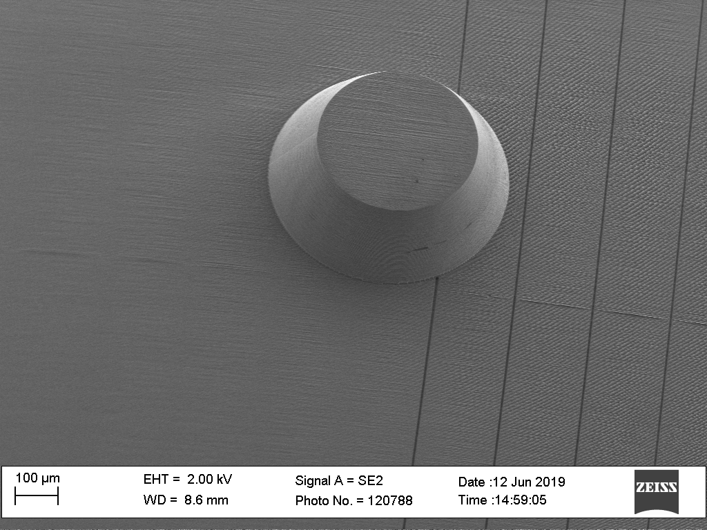
Appendix A Previous alignment approach
The initial alignment strategy was based on two wafers with alignment features integrated into one of the wafers as illustrated in Figure 12 a.). The alignment features were small cones rising from the wafers top plane, which means that the material around them and over the full surface () of the wafer has to be removed by femtosecond laser machining. Panel b.) in Figure 12 shows a detailed drawing of one of this cones. Due to the removal of a large quantity of material, the thickness of the wafer carrying the alignment features varies by more than and the surface roughness exceeds the one described in the main text (section II.2) by a factor of 10 (see Figure 12 d.)). Due to stress that appeared during laser engraving the machined surface also showed the characteristic grooves described in section II.2 as one can see in Figure 12 c.). Furthermore, we have observed a bending of the wafer which led to a variation of the distance between stacked wafers of more than .