Nanocrystalline diamond-glass platform for the development of three-dimensional micro- and nanodevices
Mathematics, Mechanics, and Materials Unit (MMMU), Okinawa Institute of Science and Technology Graduate University (OIST), 1919-1 Tancha, Onna-son, Kunigami-gun, Okinawa, Japan 904-0495
Low-cost and robust platforms are key for the development of next-generation 3D micro- and nanodevices. To fabricate such platforms, nanocrystalline diamond (NCD) is a highly appealing material due to its biocompatibility, robustness, and mechanical, electrical, electrochemical, and optical properties, while glass substrates with through vias are ideal interposers for 3D integration due to the excellent properties of glass. However, developing devices that are comprised of NCD films and through glass vias (TGVs) has rarely been attempted due to a lack of effective process strategies. In this work, a low-cost process — free of photolithography and transfer-printing — for fabricating arrays of TGVs that are sealed with suspended portions of an ultra-thin NCD film on one side is presented. These highly transparent structures may serve as a platform for the development of microwells for single-cell culture and analysis, 3D integrated devices such as microelectrodes, and quantum technologies. The process is demonstrated by fabricating TGVs that are sealed with an NCD film of thickness 175 nm and diameter 60 m. The technology described can be extended by replacing NCD with silicon nitride or silicon carbide, allowing for the development of complex heterogenous structures on the small scale.
Keywords: nanocrystalline diamond, through glass vias, glass etching, laser ablation, microfabrication ††Email address: stoffel.janssens@oist.jp (S. D. Janssens).
1 Introduction
Nanocrystalline diamond (NCD) is a highly appealing material for a variety of applications due to its biocompatibility, robustness, and mechanical, electrical, electrochemical, and optical properties. At odds with the general misconception that diamond is expensive, diamond films can be grown at low cost with microwave plasma assisted chemical vapor deposition (MWPACVD) [1]. For NCD, this can be done on large area substrates using an inexpensive precursor mixture, consisting usually of methane gas diluted in molecular hydrogen, after the deposition of diamond seeds of diameter below 10 nm [2]. During growth, a boron-containing precursor can also be added to make p-type diamond that exhibits metallic properties when heavily doped [3, 4]. Boron-doped NCD can have a relatively wide potential window [5] which, in combination with the chemical inertness and biocompatibility of diamond [6], makes it an attractive material for electrodes [7, 8]. During growth, dopants such as nitrogen and silicon can also be incorporated in diamond to form color centers for quantum technologies [9, 10]. After growth, NCD films can be processed to form two or three-dimensional suspended structures [11, 12] and the surface of an NCD film can be functionalized with a variety of (bio)molecules for use in biosensors [13] and solar cells [14]. Due to these excellent properties, NCD based devices such as micromechanical resonators of high -factor [15, 16], pressure sensors for harsh environments [17, 18], tunable optical lenses [19], biosensors that, for example, can detect influenza [20, 21], optically transparent electrodes [22, 23], CO2 reducing electrodes [24], superconducting quantum interference devices [25], and conducting atomic force microscope tips are being developed [26].
For the fabrication of 3D structures in microdevices, interposing glass layers with through holes that serve as conduits for fluids or electrical connections to thin films are indispensable [27, 28, 29]. In recent years, these interposing layers have been made available by several companies in the form of thin glass substrates with through glass vias (TGVs). Being inexpensive, transparent, electrically insulating, chemically inert, biocompatible, of high mechanical stiffness, and reusable, glass is a natural choice for the fabrication of interposing layers [30]. For example, it was recently shown that the use of TGVs can lead to low-loss and high-linearity radio frequency interposers [31]. Moreover, the properties of glass are strongly tunable. It can, for example, be made with coefficients of thermal expansion similar to those of semiconductor materials such as silicon and can thus be used to fabricate microdevices with minimal residual stress [32]. Work disclosed by Corning shows that a viable process for fabricating TGVs is based on wet etching and either laser ablation or the modification of glass with laser light [33, 34], while AGC relies on a process that is based on a focused electrical discharging method [35]. Recent work by Sato et al. [36] shows that laser ablation is promising for the fabrication of TGVs in polymer-laminated thin glass substrates. The polymer acts as a support for the thin glass plate [30].
Towards the development of devices that rely on the exceptional properties of glass and NCD, we present a low-cost process, free of photolithography and transfer printing, for fabricating arrays of TGVs that are sealed on one side with suspended portions of an ultra-thin NCD film. The resulting platform can be useful for single-cell culture and analysis when the NCD film is made porous, which can be achieved through annealing [37], and thus, be used for nutrient or drug delivery. From work on the fabrication of robust membranes by Salminen et al. [38], it is also clear that our platform has a future in the field of modeling vascular systems. When made with boron-doped NCD films, our platform can be used to construct electrodes for microfluidic channels. Alternatively, if comprised of NCD with properly arranged lattice defects, our platform can also be used for quantum technologies. It is also noteworthy that NCD can be replaced by other materials that are resistant to hydrofluoric acid (HF), such as silicon carbide or silicon nitride, and that their thermal properties, along with those of the glass that we use, allow for the fabrication of MEMS that can operate in air up to temperatures of about 400 C.
2 Materials and methods
2.1 Process overview
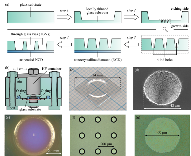
Fig. 1.a shows a schematic of the cross-section of a glass substrate before and after each fabrication step. See the figure caption for a brief description of each step. A schematic of the home-built chemical reactor used to etch glass substrates appears in Fig. 1.b and sample images at each stage of the fabrication process appear in Figs. 1.c–g.
2.2 Glass substrates and etching
| Properties | Types of glass | ||||
|---|---|---|---|---|---|
| Schott AF45 | AGC AN100 | Corning Lotus NXT | Corning Eagle 2000 | AGC Fused Silica | |
| Annealing point† [C] | 663 | 720 | 806 | 722 | 1120 |
| [ °C-1] | 4.5 | 3.8 | 3.5 | 3.2 | 0.6 |
| Density (25 C) [g cm-3] | 2.72 | 2.51 | 2.59 | 2.37 | 2.20 |
| Resistivity (250 C) [ cm] | |||||
| Young’s modulus (25 C) [GPa] | 66 | 77 | 83 | 71 | 74 |
†The temperature at which the viscosity of the glass is 1013 Pa s.
‡Linear coefficient of thermal expansion averaged from 0 to 300 C. For diamond, the value for this property is approximately °C-1 [39].
To yield mm3 substrates, a 200 m thick plate of Corning Lotus NXT glass, which is an alkaline earth boro-aluminosilicate, was diced with a Disco DAD322. The plate was purchased from the company Kuramoto. After dicing the plate, the substrates were cleaned for 20 min in acetone with an ultrasonicator. The remaining acetone was rinsed from the substrates with deionized water. The properties of Lotus NXT glass are listed in Table 1.
Isotropic etching of silicon dioxide-based glass is typically done with HF. The overall chemical reaction for etching silicon dioxide glass with HF is
| (1) |
This, however, represents a simplification of what occurs during the etching steps of our process. Moreover, no clear mechanism for glass etching is provided in literature [40]. The etching rate of silicon dioxide-based glass with HF typically increases with temperature, hydrogen fluoride concentration, and the concentration of species other than silicon dioxide [40, 41, 42]. To synthesize a silicon dioxide-based glass with specific properties, well-defined amounts of oxides such as Al2O3, As2O3, B2O3, CaO, K2O, MnO, Na2O, and P2O5 are mixed with SiO2 [40]. According to Tay et al. [42], these oxides react with HF to form fluorides that are insoluble in HF and which sediment onto portions of the etching surface leading to roughening. Iliescu et al. [43] found that adding hydrochloric acid to HF provides an effective way to dissolve these fluorides. In addition, Ceyssens and Puers [44] noted that the sedimentation of these fluorides can be avoided by vertically orienting the glass surface that is being etched. They reasoned that gravity drags the fluorides away from the surface, preventing masking.
In this work, glass etching was done in a class 1000 cleanroom at a temperature of 23 C and a humidity of 60%. In step 1, 0.6 ml of 48 m% HF was used. Since the etching rate for 48 m% HF was found to be too high for controlled etching in step 4, 11 m% HF was used in that step.
2.3 Laser ablation
Blind holes were made with a LightFab system designed for selective laser-induced etching of fused silica [45, 46]. The LightFab system was equipped with a 4 W laser. The laser light, of wavelength 1030 nm, was focused with a microscope objective to a spot of approximate diameter 1 m. The objective had a numerical aperture of 0.4, magnified 20 times, and had a working distance of 10 mm. The galvo scanner head of the system allowed the focal plane to move in three dimensions and with a stepper motor. The stage of the system could also move in three dimensions. The front side laser ablation technique was used to create blind holes where the substrate was etched maximally to approximately 50 m. Due to software restrictions, the depth of , measured relative to the surface located at the etching side of the substrate, was changed with the stepper motor rather than with the galvo. We found that crack formation during ablation was minimized by using a laser pulse frequency of 500 kHz, a pulse duration of approximately 270 fs, and a write speed of 150 mm s-1. With these parameters, the ablation threshold of the glass surface was found to occur at , where denotes the laser power scaled by the maximum laser power. The pattern that was written during laser ablation consists of 20 concentric circles each of which is separated from its immediate neighbors by 1 m. The largest circle was of diameter 40 m, whilst the smallest circle is of diameter 2 m, and the sequence of writing was from the circle of largest diameter to the circle of smallest diameter. To create holes, we sequentially wrote the pattern and lowered to a prescribed .
2.4 NCD growth
During the chemical vapor deposition of an NCD film, temperature of the substrate during growth typically ranges from 500 C to 900 C [47]. For our purposes, glasses with annealing points above 500 C are therefore preferable. To avoid stress due to thermal mismatch between the glass and the NCD, the glass should also be designed so that its coefficient of thermal expansion is equal to that of NCD for the complete range of temperatures achieved during the growth process, a criterion that can be difficult to meet. However, such glass is not currently available commercially. Still, several types of silicon dioxide-based glass on which NCD can be grown have annealing points above 500 C. Glasses that can be used for NCD growth are listed in Table 1, together with some of their salient properties. Except for fused silica, the glasses listed in this table are designed to be used in conjunction with silicon.
Preceding NCD growth, the substrate was cleaned using the first, third, and fourth steps of the RCA method. After cleaning, the surface on the growth side was seeded [2] with detonation nanodiamonds of diameter below 10 nm. Although nanodiamonds are chemically bonded to a matrix of sp2 hybridised carbon after synthesis, they can be separated by bead milling [48]. With a powder of such separated nanodiamonds, purchased from NanoCarbon Research Institute Co., Ltd., we next made a stable colloidal suspension using a method similar to that reported by Ozawa and coworkers [49]. We did this by first mixing 0.1 g of the powder in 0.2 l water ( m%) and then ultrasonicating the mixture using an ultrasonic probe with a tip of diameter 3.2 mm and length 4.5 cm. The probe was connected to a transducer of power 100 W and frequency 20 kHz that was set to cycle on and off every second for 90 minutes. The obtained suspension was turbid but cleared after a week with the settling of particles. After mounting the substrate on a spin coater, 40 l of the suspension was drop cast on the substrate. Alternatives to drop casting involve submerging the substrate in the suspension or squirting the suspension on the substrate [2, 50]. One minute after drop casting, the surface of the substrate was flushed for 10 s with deionized water while the substrate was spinning at 4000 rpm. This strategy was used to avoid any aggregation of nanodiamonds. Simply dipping the substrate in an abundance of deionized water also leads to satisfying results; this, however, can lead to unintentional seeding of substrate surfaces that should remain unseeded. After flushing, the substrate was dried by spinning for an additional 15 s without changing the spin frequency.
The seeded substrate was placed in the reactor of an SDS6500X MWPACVD system on a molybdenum substrate holder of 58 mm diameter and 5.5 mm thickness. Subsequently, the gasses in the reactor were evacuated by a Kashiyama SDE90X dry pump to base pressure 8.5 Pa. Hydrogen gas and methane gas were next introduced into the reactor at respective flow rates of 294 sccm and 6 sccm. After reaching a stable operation pressure kPa, the gasses were ignited into a plasma with 1.5 kW of 2.45 GHz microwaves. At these conditions, remained relatively far below the annealing point of Corning Lotus NXT glass, which is 722 C, and the growth rate was on the order of 1 nm min-1. This value of typically occurs at relatively low values of and . The thicknesses of the NCD films were measured during growth with a home-built interferometer. During growth, a light gray film, consisting likely of hydrogenated carbon, was unintentionally deposited on the etching side of the substrate. Within a minute, this film was removed in the reactor of a Yamato PR200 system.
2.5 Characterization
All photographic images were taken with a Canon EOS 5D camera and a Canon MP-E 65 mm lens. Surface profile features with lengths greater than 1 mm were taken with a DektakXT stylus profilometer and surface profile features with lengths less than 1 mm were taken with a Keyence VK-X150 laser microscope. From surface profiles that were taken with this microscope, the arithmetic average surface roughness was deduced. The VK-X150 was also used to measure the thicknesses of the glass substrates, taking into account the refractive index, 1.53, of the glass substrate. The VK-X150 was also used as a reflected light microscope and a Meiji MT9930L was used to perform dark-field microscopy. The thicknesses of the NCD films were measured with higher resolution than during growth using a Hamamatsu C13027 optical nano gauge. A FEI Quanta 250 FEG and a JEOL JSM-7900F SEM were used to examine the blind holes, the NCD films, and the TGVs. Grazing incidence X-ray diffraction measurements were carried out on the NCD films with a Bruker D8 Discover diffractometer, using Cu Kα X-rays of 0.15418 nm average wavelength. The angle of incidence of the X-ray beam with the samples was 0.5, which is slightly above the critical angle of total external reflection for an diamond–air interface. Raman spectra were measured on a Tokyo Instruments Nanofinder 30 system. Specifically, a 5 mW 532 nm laser was focused by an objective lens on the sample to a spot of a few micrometers in diameter, which magnifies 100 times and has a numerical aperture of 0.95. Pressure was applied to the platform as described in previous work [18]. Functions were fitted to data using the lmfit Python library.
3 Results and discussions
3.1 Glass etching
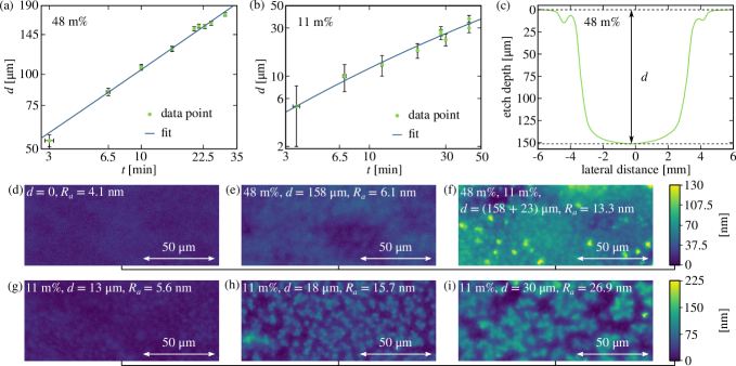
We performed systematic studies to determine the etching times for steps 1 and 4. The results for 48 m% and 11 m% HF are presented in Figs. 2.a and b respectively, which show the maximum etch depth that is reached as a function of time for each of these concentrations. Each data point on the log–log graphs represents one experiment and and have respective errors of approximately s and 3 m. Fig. 2.c shows a typical surface profile taken after etching a substrate. To predict the time that is necessary to etch a certain depth , we adapt a model that was first used to describe the oxidation of silicon [51]. The model assumes steady-state diffusion, a first order chemical reaction, and a concentration of HF at that is constant with . Under these assumptions, the time-evolution of the depth is
| (2) |
with
| (3) |
where , , and respectively denote the product of a stoichiometric constant and the concentration of species in glass that react with HF, the reaction constant, and a diffusion coefficient. Since most of these parameters are unknown, we fit the data in Figs. 2.a–b with Eq. 2. Results are provided in the caption of Fig. 2. We find that step 1 and step 4 can be performed in no more than 25 min and 35 min, respectively. During etching, a crust of fluorides forms on the surface of the glass substrate. After etching, that crust is removed by rinsing with deionized water.
Using Eq. 2, it can be found that for a reaction limited process and that for a diffusion limited process [51]. When fitting the general relation for a power law to the data for 48 m% HF etching, we find that the power of is , from which we infer that the etching process is diffusion limited. For 11 m% HF etching, we find that the power of is , which indicates that the etch process is on the border between reaction limited and diffusion limited. To understand the effect of HF concentration and duration on the etching process, we exploit the Damköhler number
| (4) |
This dimensionless quantity relates the reaction rate to the diffusion rate as follows: for , the etching process is diffusion limited; for , the etching process is reaction limited. From Eq. 4, we find that the glass etching process is reaction limited for relatively small values of but becomes diffusion limited for relatively large values of . We also infer that, consistent with our observations, diffusion limited behavior is achieved more rapidly for higher initial concentrations of HF.
The effect of HF etching on the surface roughness of a glass substrate was also investigated. This was done because rough surfaces scatter light, adversely affecting transparency. Prior to etching, the value of for a glass substrate was approximately 4 nm or less. During etching in step 1, increased up to 6 nm in the vicinity where was measured. Moreover, during etching in step 4, increased to approximately 13 nm. This cumulative increase in is evident in Figs. 2.d–f, which depict the surface profile of the glass substrate before step 1, between steps 1 and 2, and after step 4, respectively. It is remarkable that increased strongly after step 4, during which only approximately 25 m was etched. To provide additional proof that etching Lotus NXT glass with 11 m% HF induced more surface roughness than with 48 m% HF, we present in Figs. 2.g–i the surface profiles of glass substrates etched with 11 m% HF to depths of approximately 13 m, 18 m, and 30 m. More surface profiles of etched glass substrates can be found as supplementary material. The mechanism underlying this observation is not yet understood. Assuming that masking of insoluble fluorides, which are sedimented at the HF–glass interface, causes roughening during etching, we hypothesize that for etching with 48 m% HF, the velocity of the HF–glass interface is larger than the sedimentation rate of fluorides. Since step 4 required shallow etching with 11 m% HF, the surface roughness of the glass substrate after etching was relatively low.
3.2 Blind holes
| Depth of a blind hole [m] | |||||
|---|---|---|---|---|---|
| [m] | |||||
| 15 | 20 | 25 | 30 | 35 | |
| 0.36 | 21 | 24 | 28 | 31 | 33 |
| 0.38 | 25 | 28 | 32 | 36 | 39 |
| 0.40 | 28 | 31 | 35 | 38 | 48 |
| 0.42 | 31 | 34 | 38 | 43 | 47 |
| 0.44 | 34 | 38 | 42 | 47 | 49 |
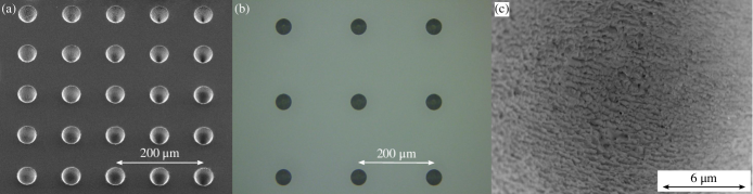
During the process of optimizing the parameters for laser ablation, we observed that crack formation becomes more apparent with increasing laser pulse frequency and . To create blind holes at the lowest value of possible and thereby avoid crack formation, we performed a study in which the depth of a blind hole was measured as a function of for various choices of depth . Results from this study are shown in Table 2 and an SEM image of the holes, taken under a tilt of 25, from which the data is obtained, is shown in Fig. 3.a. The procedure of making the holes is explained in the caption of that figure. From this study, it is clear that for m the lowest value of at which blind holes of approximately 40 m deep can be made is 0.38. Fig. 3.b shows a reflected light microscope image of an array of 9 blind holes of approximately 42 m diameter and approximately 36 m deep in a substrate that is locally etched to a thickness of 46 m. These blind holes were made with and . The values listed in Table 2 are visualized by a graph provided as supplementary material. Fig. 1.d shows an SEM image, taken under a tilt of 25, of a blind hole similar to those in Fig. 3.b. From the image, it is clear that the shape of the blind hole resembles that of a paraboloid. This is most likely a consequence of laser light shading by the glass substrate. Fig. 3.c shows an SEM image of the surface at the deepest point of the blind hole. Cracks caused by laser ablation are not detected from this image. After laser ablation, the thickness of the substrate at the deepest point of a blind hole was approximately 10 m. It is important to recognize that the the growth side does not show damage due to the laser ablation process.
3.3 Nanocrystalline diamond
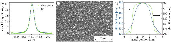
In step 3 of our process, an NCD film was grown on the surface of a glass substrate with blind holes on the growth side. During growth, the etching side was not in direct contact with the cooled substrate holder of the CVD system. An X-ray crystallography study, from which the results are shown in Fig. 4.a, confirms that crystalline films were obtained. From the lattice parameters of diamond [52], we deduce that the peak is caused by (111) crystal planes of diamond that are compressively strained by 0.1%. Results from a Raman spectroscopy study that is included in the supplementary material support these findings. A diffractogram for the (220) and (311) peaks, which are about an order of magnitude smaller than the (111) peak, is not provided due to long integration times. Fig. 1.e shows a photograph of a substrate after NCD growth that was taken with the camera located on the growth side. The substrate was placed on a mirror and therefore a large part of the light recorded by the camera was scattered, making it possible to observe the array of 9 blind holes. Fig. 4.b shows an SEM image of the NCD film, which exhibits a pinhole-free nanocrystalline structure. SEM images of this film taken with different magnifications are provided as supplementary material. Fig. 4.c show the thickness of the film together with the thickness of the glass substrate. At the thinnest part of the glass substrate, in the vicinity of the blind holes, the film shown is nm and reduces from that area radially towards the edges of the diamond film to approximately nm. Due to thin-film interference [53], the variations in film thickness are observable from differences in the apparent color of the NCD film, as shown in Fig. 1.e.
To explain variations in the thickness of the NCD film, which is depicted in Fig. 4.c, we note that, during NCD growth, only the glass substrate surface on the etching side, where no thinning is performed, is in contact with the water-cooled substrate holder whilst the glass substrate surface on the opposite growth side is in contact with a plasma. It is therefore reasonable to assume that during growth, the temperature of the etched part of the glass substrate is greater than that of the remainder of the substrate. Following Tsugawa et al. [54], who claim that the growth rate of diamond increases monotonically with , following an Arrhenius-type equation
| (5) |
where , , and respectively denote a pre-exponential factor, the activation energy, and the Boltzmann constant, we propose that the growth rate of the NCD film is spatially nonuniform. Since the growth time at all locations is the same, a nonuniform film thickness is expected. By growing the NCD film before etching, variations in film thickness can be avoided. However, it is known that NCD can be transformed into CO2 at temperatures above C [37]. The question of whether or not the heat generated during the laser ablation process induces such temperatures and affects the NCD remains to be investigated. It is worth noting that the substrate is an oxide and therefore barely interacts with air. Also, the softening point of the substrate lays at C, which makes it resilient against relatively high temperatures.
3.4 Through glass vias
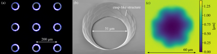
In step 4 of our process, the glass substrate is further etched by HF to form through glass vias (TGVs) that are sealed with suspended portions of an NCD film of approximate diameter 60 m. Fig. 1.f shows a micrograph, which is taken on the etching side, of nine TGVs sealed with suspended NCD of thickness nm. In the vicinity of these TGVs, the substrate is of approximate thickness 23 m and light scattering causes the walls of the TGVs to appear as black circles. Fig. 5.a is a dark-field optical microscope image, taken on the growth side of the substrate, that captures the same NCD-glass platform as Fig. 1.f. From this image, we infer that, despite the walls of the TGVs, the platform barely scatters light. Fig. 1.g shows a micrograph taken on the growth side. The circular shape represents the suspended portion of the NCD film. Fig. 5.b depicts an SEM image of the center TGV, which is taken on the etching side of the substrate, under a tilt of 25. The wall of the TGV is clearly rougher than the rest of the structure. All TGVs are tapered from the etching side towards the growth side and have minimum and maximum diameters of approximately 50 m and 80 m, respectively. Since the diameter of the suspended film is approximately 60 m, the NCD film is underetched by approximately 5 m. Fig. 5.c depicts the surface profile of a portion of the NCD film that seals the central TGV. The profile is taken on the growth side and the suspended portion of the NCD film is slightly buckled towards the glass substrate with a maximum deflection of approximately 1.25 m. This behavior is seen for all suspended portions of the NCD film that seal TGVs, as can be seen in the supplementary material. To show that the bond between the NCD film and the glass substrate is sufficiently strong for practical use, we applied a gauge pressure of 300 kPa to the suspended NCD on the etching side, the result of which was that the structure of the NCD-glass platform was able to withstand such pressures.
After laser ablation in step 2 of our process, we did not observe cracks in the blind holes; however, cusp-like structures developed on the walls of a TGV, as shown in Fig. 5.b. Spierings [40] showed that such structures typically develop from cracks during glass etching. This suggests that any cracks during the laser ablation process were too small to be detected by our imaging techniques. Still, due to the optimization of the laser ablation process, we achieved a feature size that allows the TGVs to be fairly circular. It strikes us as highly likely that using an excimer laser for laser ablation [30, 36] or activating the glass with a laser instead of performing laser ablation [34] would further reduce the roughness of the TGVs after etching. More details on modifying glass with laser light can be found in the literature [29].
During preliminary experiments, we found that NCD films, grown on fused silica substrates during step 3 of our process, completely delaminated during step 4. We suspect that this is caused by tensile stress, which is to be expected since the coefficient of thermal expansion of fused silica is less than that of diamond over the entire range of operating temperatures used during our preliminary experiments [39, 55]. Our experiments and previous work [18, 56, 57] show that NCD films grown on substrates made of any glass listed in Table 1, except fused silica, are compressively stressed, which leads us to suspect that the coefficients of thermal expansion of those types of glass might be greater than that of diamond for significant portions of the temperature ranges used in the relevant growth processes. It is noteworthy that Iliescu et al. [28] and Ceyssens and Puers [44] found that compressive stress acting on films, which mask parts of glass substrates during HF etching, is preferable over tensile stress. Our findings agree with their results. A typical consequence of compressive stress is buckling [58], which is illustrated by Fig. 5.c. For several applications, buckling should be minimized by properly tuning the coefficients of thermal expansion of the film and the substrate. Since the coefficient of thermal expansion of diamond exceeds that of fused silica but is less than those of many other glasses, we are optimistic that this can be done.
4 Conclusion
We present a low-cost and robust nanocrystalline diamond-glass platform for single-cell culture and analysis, on-demand drug delivery systems, the modeling of vascular systems, microelectrodes, quantum technologies, and high-temperature MEMS. Our platform is comprised of a glass substrate with through glass vias (TGVs) that are sealed on one side with suspended portions of an ultra-thin nanocrystalline diamond (NCD) film. Our fabrication process is free of photolithography and transfer printing and is delineated in detail sufficient to allow easy replication by others. In this process, hydrofluoric acid (HF) is used to first etch one side of a mm3 Lotus NXT glass substrate to a thickness of approximately 50 m. On the same side that is etched, blind holes of approximate diameter m and approximate depth m are subsequently formed by laser ablation. After growing an NCD film of approximate thickness 175 nm on the surface opposite to the etched side, the etched side of the substrate is further etched by HF to approximately 25 m to produce the NCD sealed TGVs. Our resulting platform is highly transparent and can handle applied pressures of at least 300 kPa.
Acknowledgements
We gratefully acknowledge support from the Okinawa Institute of Science and Technology Graduate University with subsidy funding from the Cabinet Office, Government of Japan.
References
- Achard and Tallaire [2018] J. Achard and A. Tallaire. Power electronics device applications of diamond semiconductors, chapter 1, pages 1–27. Woodhead Publishing, 2018.
- Williams et al. [2007] O. A. Williams, O. Douhéret, M. Daenen, K. Haenen, E. Ōsawa, and M. Takahashi. Enhanced diamond nucleation on monodispersed nanocrystalline diamond. Chem. Phys. Lett., 445:255–258, 2007. doi: 10.1016/j.cplett.2007.07.091.
- Gajewski et al. [2009] W. Gajewski, P. Achatz, O. A. Williams, K. Haenen, E. Bustarret, M. Stutzmann, and J. A. Garrido. Electronic and optical properties of boron-doped nanocrystalline diamond films. Phys. Rev. B, 79:045206, 2009. doi: 10.1103/PhysRevB.79.045206.
- Janssens et al. [2011] S. D. Janssens, P. Pobedinskas, J. Vacík, V. Petráková, B. Ruttens, J. D’Haen, M. Nesládek, K. Haenen, and P. Wagner. Separation of intra- and intergranular magnetotransport properties in nanocrystalline diamond films on the metallic side of the metal–insulator transition. New J. Phys., 13:083008, 2011. doi: 10.1088/1367-2630/13/8/083008.
- Hupert et al. [2003] M. Hupert, A. Muck, J. Wang, J. Stotter, Z. Cvackova, S. Haymond, Y. Show, and G. M. Swain. Conductive diamond thin-films in electrochemistry. Diamond Relat. Mater., 12:1940–1949, 2003. doi: 10.1016/S0925-9635(03)00260-7.
- Tang et al. [1995] L. Tang, C. Tsai, W. W. Gerberich, L. Kruckeberg, and D. R. Kania. Biocompatibility of chemical-vapour-deposited diamond. Biomaterials, 16:483–488, 1995. doi: 10.1016/0142-9612(95)98822-V.
- Härtl et al. [2004] A. Härtl, E. Schmich, J. A. Garrido, J. Hernando, S. C. R. Catharino, S. Walter, P. Feulner, A. Kromka, D. Steinmüller, and M. Stutzmann. Protein-modified nanocrystalline diamond thin films for biosensor applications. Nat. Mater., 3:736–742, 2004. doi: 10.1038/nmat1204.
- Alcaide et al. [2016] M. Alcaide, A. Taylor, M. Fjorback, V. Zachar, and C. P. Pennisi. Boron-doped nanocrystalline diamond electrodes for neural interfaces: In vivo biocompatibility evaluation. Front. Neurosci., 10:87, 2016. doi: 10.3389/fnins.2016.00087.
- Tzeng et al. [2015] Y.-K. Tzeng, P.-C. Tsai, H.-Y. Liu, O. Y. Chen, H. Hsu, F.-G. Yee, M.-S. Chang, and H.-C. Chang. Time-resolved luminescence nanothermometry with nitrogen-vacancy centers in nanodiamonds. Nano Lett., 15:3945–3952, 2015. doi: 10.1021/acs.nanolett.5b00836.
- Stehlik et al. [2017] S. Stehlik, M. Varga, P. Stenclova, L. Ondic, M. Ledinsky, J. Pangrac, O. Vanek, J. Lipov, A. Kromka, and B. Rezek. Ultrathin nanocrystalline diamond films with silicon vacancy color centers via seeding by 2 nm detonation nanodiamonds. ACS Appl. Mater. Interfaces, 9:38842–38853, 2017. doi: 10.1021/acsami.7b14436.
- Tian et al. [2017] Z. Tian, L. Zhang, Y. Fang, B. Xu, S. Tang, N. Hu, Z. An, Z. Chen, and Y. Mei. Deterministic self-rolling of ultrathin nanocrystalline diamond nanomembranes for 3d tubular/helical architecture. Adv. Mater., 29:1604572, 2017. doi: 10.1002/adma.201604572.
- Abdou et al. [2018] A. Abdou, P. Panduranga, J. Richter, E. L. H. Thomas, S. Mandal, O. A. Williams, J. Witzens, and M. P. Nezhad. Air-clad suspended nanocrystalline diamond ridge waveguides. Opt. Express, 26:13883–13890, 2018. doi: 10.1364/OE.26.013883.
- Caterino et al. [2015] R. Caterino, R. Csiki, A. Lyuleeva, J. Pfisterer, M. Wiesinger, S. D. Janssens, K. Haenen, A. Cattani-Scholz, M. Stutzmann, and J. A. Garrido. Photocurrent generation in diamond electrodes modified with reaction centers. ACS Appl. Mater. Interfaces, 7:8099–8107, 2015. doi: 10.1021/acsami.5b00711.
- Raymakers et al. [2018] J. Raymakers, H. Krysova, A. Artemenko, J. Čermák, S. S. Nicley, P. Verstappen, S. Gielen, A. Kromka, K. Haenen, L. Kavan, W. Maes, and B. Rezek. Functionalization of boron-doped diamond with a push–pull chromophore via Sonogashira and CuAAC chemistry. RSC Adv., 8:33276–33290, 2018. doi: 10.1039/C8RA07545J.
- Wang et al. [2004] J. Wang, J. E. Butler, T. Feygelson, and C. T.-C. Nguyen. 1.5-Ghz nanocrystalline diamond micromechanical disk resonator with material-matched isolating support. In 17 IEEE International Conference on Micro Electro Mechanical Systems. Maastricht MEMS 2004 Technical Digest, pages 641–644, 2004.
- Sartori et al. [2019] A. F. Sartori, P. Belardinelli, R. J. Dolleman, P. G. Steeneken, M. K. Ghatkesar, and J. G. Buijnsters. Inkjet-printed high-q nanocrystalline diamond resonators. Small, 15:1803774, 2019. doi: 10.1002/smll.201803774.
- Adamschik et al. [2001] M. Adamschik, R. Müller, P. Gluche, A. Flöter, W. Limmer, R. Sauer, and E. Kohn. Analysis of piezoresistive properties of cvd-diamond films on silicon. Diam. Relat. Mater., 10:1670–1675, 2001. doi: 10.1016/S0925-9635(01)00393-4.
- Janssens et al. [2014a] S. D. Janssens, S. Drijkoningen, and K. Haenen. Ultra-thin nanocrystalline diamond membranes as pressure sensors for harsh environments. Appl. Phys. Lett., 104:073107, 2014a. doi: 10.1063/1.4866028.
- Kriele et al. [2009] A. Kriele, O. A. Williams, M. Wolfer, D. Brink, W. Müller-Sebert, and C. E. Nebel. Tuneable optical lenses from diamond thin films. Appl. Phys. Lett., 95:031905, 2009. doi: 10.1063/1.3183534.
- Matsubara et al. [2016] T. Matsubara, M. Ujie, T. Yamamoto, M. Akahori, Y. Einaga, and T. Sato. Highly sensitive detection of influenza virus by boron-doped diamond electrode terminated with sialic acid-mimic peptide. Proc. Natl. Acad. Sci. U. S. A., 113:8981–8984, 2016. doi: 10.1073/pnas.1603609113.
- Siuzdak et al. [2019] K. Siuzdak, P. Niedziałkowski, M. Sobaszek, T. Łęga, M. Sawczak, E. Czaczyk, K. Dziąbowska, T. Ossowski, D. Nidzworski, and R. Bogdanowicz. Biomolecular influenza virus detection based on the electrochemical impedance spectroscopy using the nanocrystalline boron-doped diamond electrodes with covalently bound antibodies. Sens. Actuators, B, 280:263–271, 2019. doi: 10.1016/j.snb.2018.10.005.
- Lim et al. [2010] C. H. Y. X. Lim, Y. L. Zhong, S. Janssens, M. Nesládek, and K. P. Loh. Oxygen-terminated nanocrystalline diamond film as an efficient anode in photovoltaics. Adv. Funct. Mater., 20:1313–1318, 2010. doi: 10.1002/adfm.200902204.
- Ashcheulov et al. [2017] P. Ashcheulov, A. Taylor, J. More-Chevalier, A. Kovalenko, Z. Remeš, J. Drahokoupil, P. Hubík, L. Fekete, L. Klimša, J. Kopeček, J. Remiášová, M. Kohout, O. Frank, L. Kavan, and V. Mortet. Optically transparent composite diamond/Ti electrodes. Carbon, 119:179–189, 2017. doi: 10.1016/j.carbon.2017.04.035.
- Roy et al. [2016] N. Roy, Y. Shibano, C. Terashima, K. Katsumata, K. Nakata, T. Kondo, M. Yuasa, and A. Fujishima. Ionic-liquid-assisted selective and controlled electrochemical CO2 reduction at Cu-modified boron-doped diamond electrode. ChemElectroChem, 3:1044–1047, 2016. doi: 10.1002/celc.201600105.
- Mandal et al. [2011] S. Mandal, T. Bautze, O. A. Williams, C. Naud, É. Bustarret, F. Omnès, P. Rodière, T. Meunier, C. Bäuerle, and L. Saminadayar. The diamond superconducting quantum interference device. ACS Nano, 5:7144–7148, 2011. doi: 10.1021/nn2018396.
- Celano et al. [2018] U. Celano, F.-C. Hsia, D. Vanhaeren, K. Paredis, Torbjörn E. M. Nordling, J. G. Buijnsters, T. Hantschel, and W. Vandervorst. Mesoscopic physical removal of material using sliding nano-diamond contacts. Sci. Rep., 8:2994, 2018. doi: 10.1038/s41598-018-21171-w.
- Esashi [2008] M. Esashi. Wafer level packaging of MEMS. J. Micromech. Microeng., 18:073001, 2008. doi: 10.1088/0960-1317/18/7/073001.
- Iliescu et al. [2012] C. Iliescu, H. Taylor, M. Avram, J. Miao, and S. Franssila. A practical guide for the fabrication of microfluidic devices using glass and silicon. Biomicrofluidics, 6:016505, 2012. doi: 10.1063/1.3689939.
- Sugioka and Cheng [2014] K. Sugioka and Y. Cheng. Femtosecond laser 3D micromachining for microfluidic and optofluidic applications. Springer, 2014.
- Sukumaran et al. [2012] V. Sukumaran, T. Bandyopadhyay, V. Sundaram, and R. Tummala. Low-cost thin glass interposers as a superior alternative to silicon and organic interposers for packaging of 3-D ICs. IEEE Trans. Compon. Packag. Manuf., 2:1426–1433, 2012. doi: 10.1109/TCPMT.2012.2204392.
- Shah et al. [2018] U. Shah, J. Liljeholm, J. Campion, T. Ebefors, and J. Oberhammer. Low-loss, high-linearity RF interposers enabled by through glass vias. IEEE Microw. Wirel. Compon. Lett., 28:960–962, 2018. doi: 10.1109/LMWC.2018.2869285.
- Kazutaka et al. [2017] H. Kazutaka, N. Shuhei, and S. Yusuke. Glass substrate for micro display devices. SID Symposium Digest of Technical Papers, 48:1197–1200, 2017. doi: 10.1002/jsid.529.
- Burkett et al. [2015] R. C. Burkett, U.-B. Goers, S. O. Owusu, and T. L. Petriwsky. Methods for forming vias in glass substrates. US Patent US 2015/0060402 A1, 2015.
- Jaramillo et al. [2018] A. C. Jaramillo, Y. Jin, F. A. Kramer, E. A. Kuksenkova, D. W. Levesque, G. A. Piech, A. B. Shorey, and R. S. Wagner. Articles having holes with morphology attributes and methods for fabricating the same. US Patent US 2018/0068868 A1, 2018.
- Takahashi et al. [2013] S. Takahashi, K. Horiuchi, K. Tatsukoshi, M. Ono, N. Imajo, and T. Mobely. Development of through glass via (TGV) formation technology using electrical discharging for 2.5/3D integrated packaging. In IEEE 63 Electronic Components and Technology Conference, pages 348–352, 2013. doi: 10.1109/ECTC.2013.6575594.
- Sato et al. [2019] Y. Sato, N. Imajyo, K. Ishikawa, R. Tummala, and M. Hori. Laser-drilling formation of through-glass-via (TGV) on polymer-laminated glass. J. Mater. Sci.: Mater. Electron., 30:10183–10190, 2019. doi: 10.1007/s10854-019-01354-5.
- Kriele et al. [2011] A. Kriele, O. A. Williams, M. Wolfer, J. J. Hees, W. Smirnov, and C. E. Nebel. Formation of nano-pores in nano-crystalline diamond films. Chem. Phys. Lett., 507:253–259, 2011. doi: 10.1016/j.cplett.2011.03.089.
- Salminen et al. [2019] A. T. Salminen, J. Zhang, G. R. Madejski, T. S. Khire, R. E. Waugh, J. L. McGrath, and T. R. Gaborski. Ultrathin dual-scale nano- and microporous membranes for vascular transmigration models. Small, 15:1804111, 2019. doi: 10.1002/smll.201804111.
- Moelle et al. [1997] C. Moelle, S. Klose, F. Szücs, H. J. Fecht, C. Johnston, P. R. Chalker, and M. Werner. Measurement and calculation of the thermal expansion coefficient of diamond. Diamond Relat. Mater., 6:839–842, 1997. doi: 10.1016/S0925-9635(96)00674-7.
- Spierings [1993] G. A. C. M. Spierings. Wet chemical etching of silicate glasses in hydrofluoric acid based solutions. J. Mater. Sci., 28:6261–6273, 1993. doi: 10.1007/BF01352182.
- Liang and Readey [1987] D.-T. Liang and D. W. Readey. Dissolution kinetics of crystalline and amorphous silica in hydrofluoric-hydrochloric acid mixtures. J. Am. Ceram. Soc., 70:570–577, 1987. doi: 10.1111/j.1151-2916.1987.tb05708.x.
- Tay et al. [2006] F. E. H. Tay, C. Iliescu, J. Jing, and J. Miao. Defect-free wet etching through pyrex glass using Cr/Au mask. Microsyst. Technol., 12:935–939, 2006. doi: 10.1007/s00542-006-0116-0.
- Iliescu et al. [2005] C. Iliescu, J. Jing, F. E. H. Tay, J. Miao, and T. Sun. Characterization of masking layers for deep wet etching of glass in an improved HF/HCl solution. Surf. Coat. Technol., 198:314–318, 2005. doi: 10.1016/j.surfcoat.2004.10.094.
- Ceyssens and Puers [2009] F. Ceyssens and R. Puers. Deep etching of glass wafers using sputtered molybdenum masks. J. Micromech. Microeng., 19:067001, 2009. doi: 10.1088/0960-1317/19/6/067001.
- Marcinkevičius et al. [2001] A. Marcinkevičius, S. Juodkazis, M. Watanabe, M. Miwa, S. Matsuo, H. Misawa, and J. Nishii. Femtosecond laser-assisted three-dimensional microfabrication in silica. Opt. Lett., 26:277–279, 2001. doi: 10.1364/OL.26.000277.
- Hermans et al. [2014] M. Hermans, J. Gottmann, and F. Riedel. Selective, laser-induced etching of fused silica at high scan-speeds using KOH. JLMN, 9:126–131, 2014. doi: 10.2961/jlmn.2014.02.0009.
- Koizumi et al. [2008] S. Koizumi, C. E. Nebel, and M. Nesládek. Physics and applications of CVD diamond. Wiley-VCH, 2008.
- Krüger et al. [2005] A. Krüger, F. Kataoka, M. Ozawa, T. Fujino, Y. Suzuki, A. E. Aleksenskii, A. Ya. Vul’, and E. Ōsawa. Unusually tight aggregation in detonation nanodiamond: Identification and disintegration. Carbon, 43:1722–1730, 2005. doi: 10.1016/j.carbon.2005.02.020.
- Ozawa et al. [2007] M. Ozawa, M. Inaguma, M. Takahashi, F. Kataoka, A. Krüger, and E. Ōsawa. Preparation and behavior of brownish, clear nanodiamond colloids. Adv. Mater., 19:1201–1206, 2007. doi: 10.1002/adma.200601452.
- Tsigkourakos et al. [2012] M. Tsigkourakos, T. Hantschel, S. D. Janssens, K. Haenen, and W. Vandervorst. Spin-seeding approach for diamond growth on large area silicon-wafer substrates. Phys. Status Solidi A, 209:1659–1663, 2012. doi: 10.1002/pssa.201200137.
- Deal and Grove [1965] B. E. Deal and A. S. Grove. General relationship for the thermal oxidation of silicon. J. Appl. Phys., 36:3770, 1965. doi: 10.1063/1.1713945.
- Bindzus et al. [2014] N. Bindzus, T. Straasø, N. Wahlberg, J. Becker, L. Bjerg, N. Lock, A.-C. Dippel, and B. B. Iversen. Experimental determination of core electron deformation in diamond. Acta Crystallogr., Sect. A: Found. Adv., 70:39–48, 2014. doi: 10.1107/S2053273313026600.
- Born and Wolf [2002] M. Born and E. Wolf. Principles of optics. Cambridge university press, 2002.
- Tsugawa et al. [2010] K. Tsugawa, M. Ishihara, J. Kim, Y. Koga, and M. Hasegawa. Nanocrystalline diamond film growth on plastic substrates at temperatures below 100 °C from low-temperature plasma. Phys. Rev. B, 82:125460, 2010. doi: 10.1103/PhysRevB.82.125460.
- Oishi and Kimura [1969] J. Oishi and T. Kimura. Thermal expansion of fused quartz. Metrologia, 5:50–55, 1969. doi: 10.1088/0026-1394/5/2/004.
- Janssens et al. [2014b] S. D. Janssens, S. Drijkoningen, and K. Haenen. Large piezoresistive effect in surface conductive nanocrystalline diamond. Appl. Phys. Lett., 105:101601, 2014b. doi: 10.1063/1.4895458.
- Drijkoningen et al. [2016] S. Drijkoningen, S. D. Janssens, P. Pobedinskas, S. Koizumi, M. K. Van Bael, and K. Haenen. The pressure sensitivity of wrinkled B-doped nanocrystalline diamond membranes. Sci. Rep., 6:35667, 2016. doi: 10.1038/srep35667.
- Thouless [1991] M. D. Thouless. Cracking and delamination of coatings. J. Vac. Sci. Technol., A, 9:2510–2515, 1991. doi: 10.1116/1.577265.