Excitation transport in quantum devices: analytical time-dependent non-equilibrium green function algorithm
Abstract
This research demonstrates analytical time-dependent non-equilibrium green function (TD-NEGF) algorithms to investigate dynamical functionalities of quantum devices, especially for photon-assisted transports. Together with the lumped element model, we also study the effects of transiently-transferring charges to reflect the non-conservation of charges in open quantum systems, and implement numerical calculations in hetero-junction systems composed of functional quantum devices and electrode-contacts (to the environment). The results show that (i) the current calculation by the analytical algorithms, versus those by conventional numerical integrals, presents superior numerical stability on a large-time scale, (ii) the correction of charge transfer effects can better clarify non-physical transport issues, e.g. the blocking of AC signaling under the assumption of constant device charges, (iii) the current in the long-time limit validly converges to the steady value obtained by standard time-independent density functional calculations, and (iv) the occurrence of the photon-assisted transport is well-identified.
I Introduction
Photoelectric bioengineering - the use of photoelectric semiconductors as functional entities in biological systems - is heralded as an alternative option for signaling communications between organisms and physical devices in future biomedicines. In particular, research on quantum dots bio0 ; bio1 has already revealed a variety of biologically-oriented applications, e.g. drug discovery bio2 ; bio3 , disease detection bio4 ; bio5 , protein tracking bio6 ; bio7 , and intracellular reporting bio8 ; bio9 . While a qualitative understanding of these complex processes has been accessed by perturbative electron-photon interactions associated with strong electron correlations qd_tb2 , the quantitative agreement between the first-principles theory and experiments is still unsatisfactory from the perspective of the ground-state density functional theory (DFT) qd_tb3 ; steady1 .
The majority of studies on quantum-dot electronics in recent years has focused on the time-dependent density functional theory (TDDFT) qd_tb4 , as it provides a more rigorous theoretical foundation tddft1 . Its formalism may also be easily extended to cover the interaction of electrons with light or molecular environments in open quantum systems via the time-dependent non-equilibrium green function (TDNEGF) technique thesis1 ; TDNEGF1 , e.g. for the photon-assisted transport and fluorescence of contacted atomic devices. However, issues over numerical stability and the highly-demanding computational cost WBL2 make it difficult to apply the technique in mesoscopic biological systems.
To arrive at a computationally efficient but still predictive stage, this research demonstrates analytical time-dependent non-equilibrium green function (TD-NEGF) algorithms for studying dynamical functionalities of quantum devices. Together with introducing the analytical lumped element model orth1 ; QC1 , we also consider the effects of transiently-transferring charges. Here, the lumped element model approximates a description of interactions of spatially-distributed transfer charges thesis1 into a capacitor-circuit topology, significantly enhancing computation efficiency.
Numerical calculations are implemented in hetero-junction systems composed of functional quantum devices and electrode-contacts (to the environment), as indicated in Figure 1. The central device is the Si-SiO2 core-shell quantum dot, where the core is designed in the strong confinement dimensions qd_tb4 (smaller than the Bohr radius; about 5 nm for silicon). The silicon dioxide matrix is for the design of physical properties qd_tb2 ; qd_tb3 . This work includes phosphorus impurities to enable low-voltage functionalities QD1 , and accounts for the interactions between electrode-clusters and devices through properly defined self-energies. For numerical treatments, we obtain the Kohn-Sham (KS) hamiltonian and overlap matrices of the ground-states for devices and Au electrodes by standard time-independent density functional programs siesta1 ; siesta2 . With the given and , the transient properties of quantum transports are analyzed using the present TD-NEGF algorithms TDNEGF1 ; TDNEGF2 ; codeF .
This paper is organized as follows. Section 2 describes the theoretical algorithms. Section 3 discusses the studies on numerical stability, transient-to-steady analyses, and photon-assisted transport. Section 4 presents concluding remarks. Appendix A describes the fundamental physical properties, from individual components to integrated device systems. Appendix B calculates the conductance curve of the 4,4’-Bipyridine molecule with respect to photon energies, and compares it with the Tien-Gordon approach, for the purpose of identifying excitation transport dynamics.
II Time-dependent non-equilibrium green function for quasi-one-dimensional open quantum systems
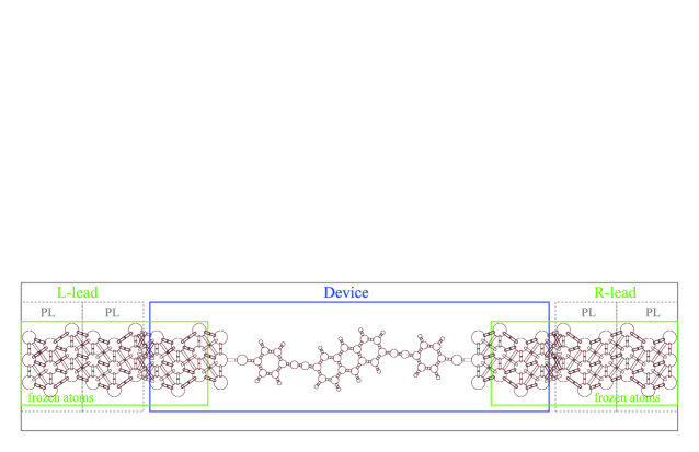
Figure 1 shows a regular open quantum system, including semi-infinite side electrodes and central quantum devices. This system is partitioned by several electronically-functional areas, named as L-electrode (L), device (D), and R-electrode (R). We describe the equation of motion (EOM) for electrons by the Heisenberg equation:
| (1) |
where is the Kohn-Sham hamiltonian matrix, and the square bracket on the right-hand side (RHS) denotes a commutator. The matrix element of the single-electron density is defined by , where and are the creation and annihilation operators for atomic orbitals and at time , respectively. On the basis of the atomic orbital sets for electrons, the matrix representation of and can be written as
| (2) |
We note that , , and () represent the matrix blocks corresponding to left-electrode , device , and right-electrode partitions, respectively. Moreover, and are ignored due to the distant separation between L and R electrodes in common applications. It is noted that the holographic electron density theorem and Runge-Gross theorem are applied for time-dependent electron dynamics TDNEGF1 ; TDNEGF2 , stating that the initial ground-state density of the subsystem can determine all physical properties of systems at any time . Hence, and can be approximately expressed as functions of for a formally closed-form equation of motion as described below.
Placing Eq. (2) into Eq. (1), we can write the equation of motion for as
| (3) | |||||
| (4) |
Here, and denote the atomic orbital in partition D, denotes the state of (=L, R) electrode, and is the dissipation term due to the contacts of the device with electrodes L and R. The transient current through an electrode’s interfaces can be calculated by:
| (5) | |||||
II.1 Expressions of the dissipation function using the Green function formalism
To calculate the dissipation term in EOM and the transient current equation, this work uses the time-dependent non-equilibrium Green function (TDNEGF) formalism. It is noted that a replacement for the overlap-matrix by the identity matrix is proceeded by redefining the device’s hamiltonian book1 (Ch. 8.1.2): . The expression of the dissipation function hence can be derived as TDNEGF1 :
| (6) |
where the lesser Green functions and the retarded Green functions in Eq. (6) are determined via Kadanoff-Baym equations TDNEGF1 ; kb1 :
| (7) | |||||
| (8) |
with notations , , and . The advanced self-energy and the lesser self-energy for electrode by definition are:
| (9) | |||||
| (10) |
Here, is the Heaviside step function, is the Kohn-Sham matrix of the isolated electrode , and is the Fermi distribution function for .
II.2 Wide-band limit approximation for the dissipation function
For efficient computations of the equation of motion in Eqs. (7) and (8), we introduce the wide-band limit (WBL) approximation WBL1 for L and R electrodes under conditions TDNEGF1 ; WBL2 : (1) the bandwidths of the electrodes are larger than the coupling strength between the device and L or R electrode; (2) the broadening matrix (the imaginary part of self-energy, as defined below) is assumed to be energy-independent, resulting in the requirement for an electrode’s density of state and device-electrode couplings to be slowly varying in energy; and (3) the level shifts of electrodes via bias are approximated to be constant for all energy levels.
Through the conditions for the wide-band limit approximation, the self-energy is split up into two real matrices: one is the hermitian matrix representing level shift, and the other is the anti-hermitian matrix representing level broadening. Specifically, Eqs. (9) and (10) are:
| (11) |
where and obey the Kramers-Kronig relation kk1 . The dissipation term for electrodes L and R now is thesis1 :
| (12) |
with the definition of as:
| (13) | |||
and
| (14) |
Together with EOM for in Eqs. (3) and (4), one is prepared to calculate the transient electron density of the device and the boundary currents in Eq. (5).
II.3 Calculations of self-energy matrices and in
In principle, we can formulate the retarded self-energy for contact with electrode in the energy domain thesis1 as:
| (15) |
Considering the semi-infinite electrodes, the periodic Au(111) lattices can be divided into principle layers (PLs) along the transport direction (see Fig 1). Here, we choose PLs to be wide enough so that only interactions between the nearest PLs need to be considered; i.e. the coupling matrix between contact and device region will be restricted to one PL. Consequently only the surface block of , i.e. the surface green function , is needed for calculating Eq. (15). This work adopts an iterative method surfG to calculate the surface green function that includes properties of the semi-infinite lattices. Specifically, we calculate the self-energy matrices and for wide-band approximation at the Fermi level as
| (16) |
II.4 Analytical formulae of the term in
On the calculation of the function in Eq. (13), this work introduces two approximations for enhancing numerical stability, accuracy, and efficiency in large(-time-space)-scale simulations:
| (19) | |||||
| (22) |
Here, is the incomplete gamma function, and is the total chemical potential for the Fermi distribution function of the electrode . For simplicity, the variable is introduced to define the effective hamiltonian. By expressing with its eigenvector matrix and the diagonal eigenvalue matrix , we can analytically rewrite equation (13):
The elements of the diagonal matrices , , and can be analytically calculated by:
| (24) |
| (26) | |||||
where the energies and are the lower integral boundary and the higher integral boundary, respectively. is the condition boundary of the approximation function in Eq. (19), and is the inverse temperature. The complex natural logarithm of denotes .
The wide-band dissipation function in Eq. (12) now can be efficiently calculated with the given device hamiltonian, the device reduced density matrix, the self-energies containing the effect of the leads, and the analytical formulae.
II.5 Correction of the device Hamiltonian for transient variations of electron densities using the lumped element model
To consider the effects of transiently-transferring charges in the open quantum system, the device hamiltonian can be expressed in the perturbative form hform1 of:
| (27) |
Here, the change of electron density can be computed via the density matrix in Eq. (3)
| (28) |
as a function of spatial variable , or, alternatively, by
| (29) |
using the atom-site notations. Here, and are the reference charges chosen for neutrality, is the device overlap matrix, and is a set of local basis functions used in the tight-binding formulation. According to the Taylor expansion of the total energy around the reference density, this change of charge density can result in corrections to the Hartree and the exchange-correlation potentials perturb1 ; perturb2 for the device hamiltonian as in Eq. (27), and it is continuously renewed with the transient density matrix in Eq. (3). Herein, we simplify the correction of the device hamiltonian by retaining only the Hartree potential (assuming the exchange-correlation term is insignificant in the mean-field criterion), which obeys the three-dimensional Poisson equation
| (30) |
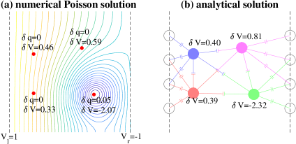
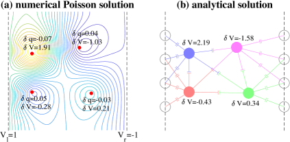
with the boundary conditions imposed by the lead potentials. Since the conventional Poisson solution is based on spatially-discretized grids ( grids for -atom systems) with numerically iterative processes, the computations can be significantly time-consuming for large systems. Thus, it is convenient to study another efficient analytical model.
On the basis of the success of the muffin-tin (MT) approximation, the total excess charge is assumed to collectively locate within a spherical region (MT-sphere) surrounding its nucleus . The interactive charges inside different MT-spheres are considered as capacitance effects datta1 . All MT-spheres (-variables) of the system construct a capacitance-circuit architecture in the lumped element model that supplies an analytical solution for the Poisson equation blockbook1 . In principle, the capacitances are treated as a combination of the electrostatic capacitance and quantum capacitance datta1 . Herein, we assume the quantum capacitance to be less dominant than the electrostatic capacitance for and ignore it in our work.
Replacing the spatial solution () of the Poisson equation by the atom-site notations () for the lumped element model orth1 ; orth2 , we can rewrite Eq. (30) by a matrix-form equation
| (31) | |||||
| (32) | |||||
| (33) |
Here, the matrix elements of are calculated in a two-center approximation as proposed in the tight-binding approach thesis1 , obeying the formal condition . The notation is the group of the first nearest-neighbor (NN) atoms in the device region for atom , and is the group of the first nearest-neighbor atoms in the lead region. Herein, defines the capacitance between two ideal metal spheres, is the spatial distance between atoms and , and is the effective muffin-tin radius for atoms and and is defined by in this work. Moreover, is the potential vector with the components being deviations of electrostatic potentials on atom-sites . is the potential of lead atom imposed by boundary conditions. is the variation of the charge density obtained by Eq. (29), and represents the defect charge for atom . By linear algebra the potential vector can be easily solved using . For instance, in a 1-dimensional homogeneous system having 4 atoms L-A-A-R, the capacitance between nearby atoms is denoted as , and the biases are denoted as and for lead atoms L and R, respectively. There are no excess charges () inside the MT-sphere of device atoms A. In this way, the 2x2 capacitance matrix has components and , and the charge vector is . One then can obtain the electrostatic potentials for the two atoms A as , which agree with the free-space Poisson solution.
Figures 2-3 illustrate 2-dimensional examples with a comparison between the numerically iterative solution and the lumped element model. In order to connect the spatial-distributive variable with the atom-site notation , we use the conventional distribution function for the density function in two-dimensional systems:
| (34) |
Here, the circular-symmetry assumption thesis1 has been adopted, where is the position for atom , and is associated with the effective radius of the MT-sphere by ( in this work). The obtained potential is projected on the atomic sites through
| (35) |
for a comparison with the lumped element model in this work. We study two exemplary structures as shown in Figs. (2-3). The analytical solution presents comparable results with that from the numerically-iterative method. It is emphasized that the analytical model turns inefficient at large biases or strong density variations, because the MT sphere cannot accurately account for the distorted and displaced distribution function of the electron density away from the nucleus.
The relevant parameters of the MT radius used in this work are MTSi ; MTO ; MTAu ; MTP , , , and . All computations are operated on a workstation having 2xCPU(E5-2690 v2) and 128G of DRAM. Fortran source codes can be downloaded online (codeF, ).
III Time-dependent electron transport in open quantum-dot systems
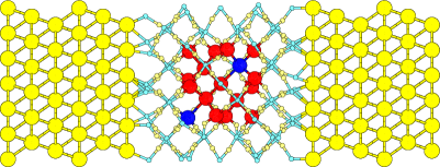
This section studies the time-dependent electron transport for open quantum-dot systems, as illustrated in Fig. 4. The Si-based quantum dot (red atoms) and SiO2 matrix (small light cyan-yellow atoms) in the device region are enclosed by two semi-infinitely long Au wires. Two dopant atoms (phosphorus; blue atoms) are placed inside the quantum dot and at the Si-SiO2 interface, respectively, according to their energetically-favored formation energyQD1 . It is assumed that the positions of the atoms of Au electrodes are under constraint by the experimental set-ups, while the atoms of the doped Si-SiO2 quantum dot are in equilibrium according to geometry relaxations. This work initially sets the distance between the nearest cross sections of silica and gold boundaries before geometry relaxations to be 1.8 .
The appendix describes in details the other relevant properties, from individual components to the integrated systems. Additional parameters and numerical techniques are as follows: time step , voltage function with , the globally-adaptive numerical integral treating Eq. (13), and the fourth-order Runge Kutta methods (RK4) for solving Eq. (3). Here, we adopt the linear extrapolation of the density matrix during the RK4 process.
III.1 Numerical stability
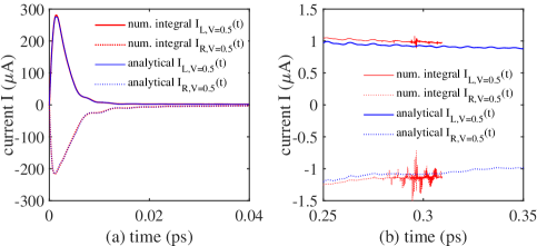
Figure 5 shows transient currents of the quantum-dot system driven by bias functions and for the left and right electrodes, respectively. Calculations by the numerical-integral technique on Eq. (13) and the analytical algorithm on Eq. (II.4) are compared during a finite time period (t0.04 ps) in Fig. 5(a) and after a long time period (t0.25 ps) in Fig. 5(b). As indicated in this figure, both methods show transient currents comparable to each other at t0.28 ps. The calculation by the numerical-integral method, however, begins to abnormally fluctuate after t0.28 ps and runs into sudden termination. The analytical algorithm presents superior numerical stability even at a large time scale, as discussed in the following paragraphs.
III.2 Transient current driven by DC bias
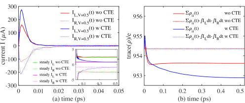
Figure 6(a) shows transient currents by analytical TD-NEGF algorithms, both including and excluding corrections of charge transfer effects (CTE). The voltage functions are set by and for the left and right electrodes, respectively. For comparison and validation, we calculate the corresponding steady currents with the Landauer Buttiker formula datta1 , an integral of the transmission functions in Fig. 14(b), using the SIESTA program. With the steady and transient results in Figure 6(a), one observes that the transient currents asymptotically approach the values of the corresponding steady solutions longtime1 ; longtime2 (see the inset diagram), no matter whether or not the charge transfer effects are synchronously considered. In fact, the inclusion of charge transfer effects presents considerable corrections for the convergence of the transient current, suggesting non-trivial influences of charges beyond the ground state approximation. The curves also depict that the calculation including CTE requires a much longer time to bring the system into the steady sate, inferring a self-consistent redistribution process of the device charge. Figure 6(b) shows the transient properties of the electron number and the integrals of boundary currents, obeying the continuity equation for the device region.
III.3 Transient current driven by AC bias
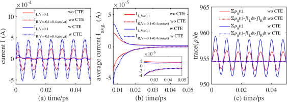
Figure 7 studies the transient currents for the quantum-dot devices driven by AC voltages. To observe the properties of charges inside the device, the voltage functions are asymmetrically set by and for the left and right electrodes, respectively. The AC frequency is Hz. It is noted that the AC signaling is only applied on the right electrode. In Fig. 7(a), the calculation including charge transfer effects exhibits an oscillating interfacial current and represents the physical AC signaling through the device. The calculation excluding charge transfer effects, however, depicts a constant interfacial current , exhibiting non-physical blocking of AC signals. Figure 7(b) studies the net current by averaging of Fig. 7(a) over one period . On the basis of the analyses above, we conclude that the charge transfer effects considerably influence the transient properties of the devices, but its significance on the steady outcomes remains unrevealed. Relevant discussions by means of photon-assisted dynamics will be discussed in the following paragraph. Here, similar to the analysis on the DC condition, Figure 7(c) monitors the validity of the algorithms by the continuity equation.
III.4 Photon-assisted transport
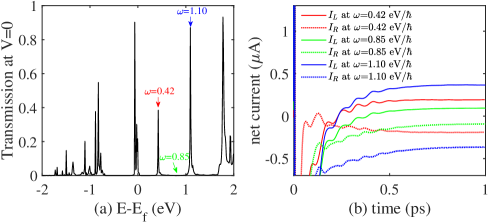
Figure 8 studies the photon-assisted transport (PAT) of the quantum-dot devices by applying AC voltages at specified frequencies. The voltage functions are set by and , with condition . To identify proper AC frequencies for photon excitations, Fig. 8(a) calculates the zero-bias transmission function. Here, we select three energy levels as , , and , representing the states inside the first excited energy-band, inside the energy gap, and inside the second excited energy-band, respectively. Figure 8(b) displays the transient net currents driven by the voltage function with given frequencies. Numerical results indicate that the photons with energies meeting excited levels ( and ) can distinctly enhance electron transport and raise the net DC current; otherwise, the photon () presents less significant influences on the current. Another exemplary device of 4,4’-Bipyridine molecules is addressed in the appendix for more detailed discussions about PAT with the Tien-Gordon approach.
IV Conclusions
This research presents analytical algorithms, with fortran codes, to study excitation transports in quantum devices. Relevant analyses show that the algorithms enable efficient and numerically-stable computations even at large time and space scales, whereas conventional treatments could suffer problems on numerical divergence and high-demanding computation cost. We also consider the effects of transiently-transferring charges, inferring to excitations or populations of electrons beyond ground states, together with a lumped element model. The validity of this work is discussed with a comparison with time-independent density functional calculations and the photon-assisted transport dynamics.
V Acknowledgement
This work was supported by ChiMei Visual Technology Corporation under Project no. 37.
Appendix A Physical properties from individual components to integrated quantum systems
A.1 Atomic Electrodes: Au(111) Nanotubes
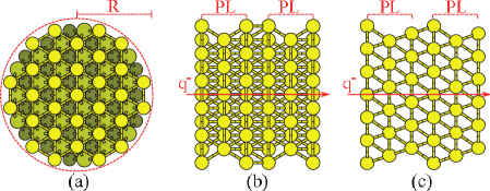
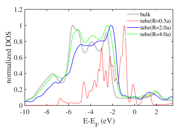
This research uses Au(111) nanotubes as atomic electrodes. The length of the Au-Au bond is determined with geometry relaxations of the Au bulk in the SIESTA programsiesta1 ; siesta2 , obtaining the value =2.8785 (lattice constant a==4.0708 , which is similar to the experimental value chembook1 of 4.0782 ). The effects of core electrons are evaluated with norm-conserving pseudopotentials in the local density approximation (Ceperley-Alder exchange-correlation potentialLDA1 ; LDA2 ), which are generated by the ATOM programatom1 ; siesta1 . The valence electrons of Au are calculated in the s-d hybridized configuration sdhybrid1 . All the calculations for nanotubes are performed on Monkhorst-Pack grids in reciprocal spaces under an electronic temperature of 300K. Figure 9 shows (a) the longitudinal perspective and (b-c) two lateral perspectives for a finite segment of Au(111) nanotubes. In actual computations, the nanotube is set as an infinite stack of principle layers (PL) along the axial (longitudinal) direction, and has cross-section radius R. Figure 10 shows the normalized density of states (DOS) for Au bulk and Au(111) nanotubes, where the radiuses of the nanotubes are set as R=0.5a, R=2.0a, and R=4.0a, respectively. Here, is the Fermi level corresponding to the mentioned system. In Fig. 10, DOS of the Au bulk shows metallic properties as the literature AuBulkDOS reports. For Au(111) nanotubes, when increasing the cross-section radius R, the DOS functions of the tubes at energies near change from discrete to uniform distributions, depicting the transfer of systems from 1D-line to 3D-bulk structures. In this work, we use Au(111) nanotubes with R=2a for semi-infinite electrodes in transport problems. This adoption (setting R=2a) meets the requirement of slowly-varying DOS for the wide-band limit (WBL) condition WBL1 , and demands computation resources that are affordable.
A.2 Doped Si-SiO2 quantum dots
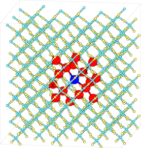
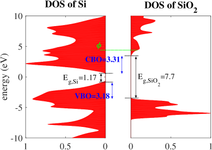
This research investigates the silicon quantum dots with diameters around 1.0 nm that are embedded in a -cristobalite SiO2 matrix. The dopant phosphorus (P) atoms are placed inside quantum dots based on their energetically-favored formation of structures QD1 (see Fig. 11). Lattice constants are determined with geometry relaxations in the SIESTA program (setting orbital bases s and p for species Si, O, and P). The obtained values are 5.5001 (5.4306 by experiment chembook1 ) for the Si diamond structure and 7.46831 (7.160-7.403 in textbooks chembook1 ; sio2a ) for -cristobalite silica. We investigate the energy band diagram of Si-SiO2-slabs heterojunctions by using Anderson’s rule through Fig. 12, in which the vacuum levels (green dotted lines) of Si and SiO2 slabs are aligned at the same energy. Here, the vacuum level is defined as the effective potential (adding local pseudopotential, Hartree potential, and exchange-correlation potential) at zero-density points near the surface of slabs having 35 atomic layers. All calculations are performed at -point of the reciprocal space. As indicated in Fig. 12, the vacuum levels are 1.064 eV and 1.626 eV for Si-slab and SiO2-slab, respectively, corresponding to working functions =4.46 eV and =4.52 eV. The experimental value chembook1 is eV. The computed energy gaps are 1.17 eV for bulk silicon and 7.7 eV for -cristobalite silica, which can be compared to the experimental values of 1.1 eV and 9.0 eV, respectively. The valence band offset (VBO) and conduction band offset (CBO) for Si-SiO2 heterojunctions are estimated to be 3.18 eV and 3.31 eV, respectively. The obtained VBO values are smaller than experimental measurements vbo1 ; vbo2 with VBO=4.6 eV and CBO=3.1 eV. Several theoretical works using hopping mechanisms QD1 ; QD2 ; QD3 give VBO2.6 eV and CBO3.9 eV.
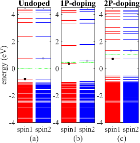
With relevant material parameters, the Si-SiO2 quantum-dot device in Fig. 11 is constructed from a supercell of -cristobalite silica by removing O atoms in a cut-off box QD1 . Figure 13 reports the eigenvalue spectra for the undoped, 1P-doping, and 2P-doping structures after relaxation processes, using the corresponding initial geometries in Fig. 11. The spectrum energies are aligned along the level of the deep valence states of SiO2, and the origin of the energy axis is determined according to the fermi level of the undoped structure. Black and gray circles mark the highest occupied molecular orbital (HOMO) and lowest unoccupied molecular orbital (LUMO) states, respectively. The green dotted line represents the fermi level of the corresponding structure.
In Fig. 13(a), the undoped quantum-dot structure exhibits a distinguished energy spectrum from that of the slab-heterojunction in Fig. 12, revealing the interfacially strain-related electron levels mismatch1 . For the 1P-doping system, the odd number of electrons leads to the spin-dependent energy spectrum in Fig. 13(b), which depicts a clear donor behavior and agrees well with previous works QD1 ; donor1 . This study adopts the 2P-dopping structure in Fig. 13(c) due to the following considerations: (i) has lower threshold voltage owing to the rising fermi level and the decreasing energy gap, compared to the other two structures; and (ii) has spin independence for reduced dimensions of the atomic orbital sets and the negligible spin-flip mechanism.
A.3 Transmission function of the open quantum-dot system
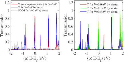
The complete open quantum-dot system is depicted in Fig. 4. Its transmission function T (blue curve) is calculated by SIESTA::Transiesta programs, and is compared with the projected density of the state (PDOS; gray curve) of the Si-SiO2 quantum dot, as shown in Fig. 14(a). The red-curve is calculated by fortran program using the tight-binding formulation. In Fig. 14(b), the transmission functions for the system with different biases are computed by SIESTA, signifying the effects of non-conserved charges in open quantum systems.
Appendix B Photon-assisted transport in 4,4’-Bipyridine molecules
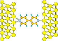
This appendix discusses photon assisted transport in the molecule device, as illustrated in Fig. 15. The 4,4’-Bipyridine molecule in the device region is enclosed by two semi-infinitely long Au wires. It is assumed that the positions of the atoms of Au electrodes are under constraint by the experimental set-ups, while the device atoms are in equilibrium according to geometry relaxations. The distance between the nearest device atoms and gold boundaries is initially set to be 2.5 for setting weak device-electrode couplings. Parameters about the muffin-tin radius are referred to the literature mt_radius .
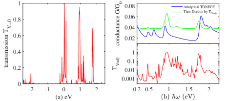
To analyze the device conductance with respect to photon energies, we set the voltage functions by and , with condition . Figure 16(a) shows the complete zero-bias transmission function of the system, depicting accessible transport channels in the molecule device. In Fig. 16(b), the upper diagram calculates the device conductance (blue curve) as a function of the photon energy using the TD-NEGF algorithm, and compares that (green curve) by the Tien-Gordon approach. Here, denotes the conductance quantum. Numerical results demonstrate that both curves show quantitative agreements in the low frequency regime. Beyond the linear response (low frequency) condition by the Tien-Gordon approximation, the conductance functions present qualitative comparability only with photon energies near primary excited energy-bands. The lower diagram in Fig. 16(b) plots the corresponding log-scale transmission curve, which is similar to that via TD-NEGF algorithms.
References
- (1) L. Ostrovska, A. Broz, A. Fucikova, T. Belinova, H. Sugimoto, T. Kanno, M. Fujii, J. Valenta, and M. H. Kalbacova, RSC Advances 6 (2016), 63403.
- (2) S. J. Rosenthal, J. C. Chang, O. Kovtun, J. R. McBride, I. D. Tomlinson, Chemistry Biology 18 (2011), 10.
- (3) S. Jin, and K. Ye, Biotechnol. Prog. 23 (2007), 32.
- (4) I. L. Medintz, H. Mattoussi, and A. R. Clapp, Int. J. Nanomed. 3 (2008), 151.
- (5) X. Michalet, F. F. Pinaud, L. A. Bentolila, J. M. Tsay, S. Doose, J. J. Li, G. Sundaresan, A. M. Wu, S. S. Gambhir, and S. Weiss, Science 307 (2005), 538.
- (6) X. Gao, Y. Cui, R. M. Levenson, L. W. K. Chung, and S. Nie, Nat. Biotech. 22 (2004), 969.
- (7) T. Pons, and H. Mattoussi, Ann. Biomed. Eng. 37 (2009), 1934.
- (8) F. Pinaud, S. Clarke, A. Sittner, and M. Dahan, Nat. Meth. 7 (2010), 275.
- (9) A. M. Derfus, W. C. W. Chan, and S. N. Bhatia, Adv. Mat. 16 (2004), 961.
- (10) G. Ruan, A. Agrawal, A. I. Marcus, and S. Nie, J. Am. Chem. Soc. 129 (2007), 14759.
- (11) H. Dong, T. Hou, X. Sun, Y. Li, and S. T. Lee, Appl. Phys. Lett. 103 (2013), 123115.
- (12) Y. Matsumoto, A. Dutt, G. S. Rodrıguez, J. S. Salazar, and M. A. Mijares, Appl. Phys. Lett. 106 (2015), 171912.
- (13) S. M. Lindsay, and M. A. Ratner, Adv. Mater. 19 (2007), 23.
- (14) S. Nazemi, M. Pourfath, E. A. Soleimani, and H. Kosina, J. App. Phys. 119 (2016), 144302.
- (15) G. Stefanucci, C.O. Almbladh, Phys. Rev. B 69 (2004), 195318.
- (16) Y. Wang, C. Y. Yam, Th. Frauenheim, G.H. Chen, T.A. Niehaus, Chemical Physics 391 (2011), 69.
- (17) X. Zheng, F. Wang, C. Y. Yam, Y. Mo, and G. H. Chen, Phys. Rev. B 75 (2007), 195127.
- (18) Christian Oppenlander, Time-dependent density functional tight binding combined with the Liouville-von Neumann equation applied to AC transport in molecular electronics, Dissertation, Faculty of Physics, University of Regensburg, (2014).
- (19) J. A. Melsen, U. Hanke, H. O. Muller, and K. A. Chao, Phys. Rev. B 55 (1997),10638.
- (20) I. L. Ho, T. H. Chou, and Y. C. Chang, Comput. Phys. Commun. 185 (2014), 1383.
- (21) N. Garcia-Castello, S. Illera, J. D. Prades, S. Ossicini, A. Cirera, and R. Guerra, Nanoscale 7 (2015), 12564.
- (22) J. M. Soler, E. Artacho, J. D. Gale, A. Garcia, J. Junquera, P. Ordejon and D. Sanchez-Portal, J. Phys.: Condens. Matter 14 (2002), 2745.
- (23) P. Ordejon, E. Artacho and J. M. Soler, Phys. Rev. B: Condens. Matter 53 (1996), R10441.
- (24) E. Runge and E. K. U. Gross, Phys. Rev. Lett. 52 (1984), 997.
- (25) submitting
- (26) J. C. Cuevas, and E. Scheer, Molecular Electronics: An Introduction to Theory and Experiment, World Scientific (2010).
- (27) R. Tuovinen, E. Perfetto, G. Stefanucci, and R. van Leeuwen, Phys. Rev. B 89 (2014), 085131.
- (28) A. P. Jauho, N. S. Wingreen, and Y. Meir, Phys. Rev. B 50 (1994), 5528.
- (29) S. Yokojima, G. Chen, R. Xu, and Y. Yan, Chem. Phys. Lett., 369 (2003), 495.
- (30) M. P. Lopez-Sancho, J. M. Lopez-Sancho, and J. Rubio, J. Phys. F: Met. Phys. 14 (1984), 1205; 15 (1985), 851.
- (31) A. Pecchia, G. Penazzi, L. Salvucci, and A. D. Carlo, New J. Phys. 10 (2008), 065022.
- (32) W. M. C. Foulkes and R. Haydock, Phys. Rev. B 39 (1989), 12520.
- (33) M. Elstner, D. Porezag, G. Jungnickel, J. Elsner, M. Haugk, Th. Frauenheim, S. Suhai, and G. Seifert, Phys. Rev. B 58 (1998), 7260.
- (34) S. Datta, Quantum Transport: Atom to Transistor, New York, Cambridge University Press (2005).
- (35) H. Grabert, and M. H. Devoret,Single Charge Tunneling: Coulomb Blockade Phenomena In Nanostructures, New York, Springer Science Business Media (1992).
- (36) I. L. Ho, D. S. Chung, M. T. Lee, C. S. Wu, Y. C. Chang, and C. D. Chen, J. Appl. Phys. 111 (2012), 064501.
- (37) H. Dreysse (editor), Electronic Structure and Physical Properties of Solids: The Uses of the LMTO Method, p. 122, Springer-Verlag, Berlin Heidelberg (2000).
- (38) G. Nazir, A. Ahmad, M. F. Khan, and S. Tariq, Comp. Cond. Mat. 4 (2015), 32.
- (39) M. F. Thomas, J. M. Williams, and T. C. Gibb (editors), Hyperfine interactions (C), p. 186, Springer Science Business Media Dordrecht (2002).
- (40) Z. Dai, W. Jin, J. X. Yu, M. Grady, J. T. Sadowski, Y. D. Kim, J. Hone, J. I. Dadap, J. Zang, R. M. Osgood, Jr., and K. Pohl, Phys. Rev. Materials 1 (2017), 074003.
- (41) C. Yam, X. Zheng, G. Chen, Y. Wang, T. Frauenheim, and T. A. Niehaus, Phys. Rev. B 83 (2011), 245448.
- (42) C. Oppenlander, B. Korff, and T. A. Niehaus, J. Comput. Elec. 12 (2013), 420.
- (43) W. M. Haynes, CRC Handbook of Chemistry and Physics, CRC Press, Taylor Francis Group (2017).
- (44) D. M. Ceperley and B. J. Alder, Phys. Rev. Lett. 45 (1980), 566.
- (45) J. P. Perdew and A. Zunger, Phys. Rev. B: Condens. Matter 23 (1981), 5048.
- (46) M. C. Payne, M. P. Teter, D. C. Allan, T. A. Arias and J. D. Joannopoulos, Rev. Mod. Phys. 64 (1992), 1045.
- (47) L. S. Wang, Phys. Chem. Chem. Phys. 12 (2010), 8694.
- (48) C. G. Sanchez, E. P. M. Leiva, and W. Schmickler, Electrochem. Commun. 5 (2003), 584.
- (49) C. Sevik, and C. Bulutay, J Mater. Sci. 42 (2007), 6555.
- (50) G. Conibeer, M. A. Green, D. Konig, I. Perez-Wurfl, S. Huang, X. Hao, D. Di, L. Shi, S. Shrestha, B. PuthenVeetil, Y. So, B. Zhang and Z. Wan, Prog. Photovoltaics: Res. Appl. 19 (2011), 813.
- (51) G. Seguini, S. Schamm-Chardon, P. Pellegrino and M. Perego, Appl. Phys. Lett. 99 (2011), 082107.
- (52) K. Seino, F. Bechstedt and P. Kroll, Phys. Rev. B: Condens. Matter 82 (2010), 085320.
- (53) K. Seino, F. Bechstedt and P. Kroll, Phys. Rev. B: Condens. Matter 86 (2012), 075312.
- (54) R. Guerra, E. Degoli and S. Ossicini, Phys. Rev. B: Condens. Matter 80 (2009), 155332.
- (55) M. Mavros, D. A. Micha and D. S. Kilin, J. Phys. Chem. C 115 (2011), 19529.
- (56) M. Dadsetani, and A. R. Omidi, RSC Adv. 5 (2015), 90559.