Ordered structure of FeGe2 formed during solid-phase epitaxy
Abstract
Fe3Si/Ge(Fe,Si)/Fe3Si thin film stacks were grown by a combination of molecular beam epitaxy and solid phase epitaxy (Ge on Fe3Si). The stacks were analyzed using electron microscopy, electron diffraction, and synchrotron X-ray diffraction. The Ge(Fe,Si) films crystallize in the well oriented, layered tetragonal structure FeGe2 with space group P4mm . This kind of structure does not exist as a bulk material and is stabilized by solid phase epitaxy of Ge on Fe3Si. We interpret this as an ordering phenomenon induced by minimization of the elastic energy of the epitaxial film.
Ordering phenomena of epitaxial layers have been found in semiconductor mixed crystals as well as in metallic alloys. In general, the ordering has a strong influence on the physical properties of the epitaxial films. In semiconductors (SC), the formation of monolayer superlattices in mixed crystal AlxGa1-xAs epitaxial films grown by metal-organic chemical vapor deposition on (110) or (100) oriented GaAs substrates has been observed.Kuan et al. (1985) The authors suggested that this long-range ordering is a thermodynamically stable phase at temperatures below about 800 ∘C. A strain-induced order-disorder transition was found in SiGe epitaxial films grown on Si(001) by molecular beam epitaxy (MBE).Ourmazd and Bean (1985) This phenomenon later was explained using self-consistent total energy calculations.Martins and Zunger (1986); Mbaye et al. (1987)
For metallic alloys, the amount of collected data is even larger.Gorsky (1928); Willliams (1935); Khachaturyan (1973, 1983); Ruban and Abrikosov (2008); Zhuravlev et al. (2014); Wr´obel et al. (2015) Here, the influence of ordering on material properties like hardness, conductivity, magnetism and corrosion resistance is important. The elastic interaction of the different atoms of the alloys often leads to energetically favored ordered structures. This kind of ordering is influenced by the anisotropy of the crystal lattice.
The structures of the epitaxial Ge and Fe3Si films on GaAs substrates correspond well to the known structures of their bulk materials.Tinkham et al. (2008); Jenichen et al. (2009, 2005) However, when the Fe3Si film is used as a substrate for epitaxial growth of Ge, the influence of the Fe3Si structure on the growing epitaxial Ge film unexpectedly turns out to be stronger and ordering phenomena occur. These ordering phenomena are induced by the epitaxial growth and were not observed in bulk material up to now. Several methods were applied to achieve perfect semiconducting Ge films on top of ferromagnetic (FM) layers.Yamada et al. (2012); Jenichen et al. (2014); Kawano et al. (2016) Recently, the method of solid-phase epitaxy (SPE) of Ge was utilized in order to achieve a perfect crystallinity of the film and superior interface quality.Gaucher et al. (2017); Sakai et al. (2017); Kawano et al. (2017) However, the diffusion of Fe and Si was not entirely prevented during the annealing process. Therefore, the Ge film contained some amount of Fe and Si, leading to a shift of the X-ray diffraction (XRD) peak of the Ge(Fe,Si) film and the formation of a superlattice-like structure inside the Ge(Fe,Si) film. The FM Fe3Si forms Schottky contacts with the SC Ge and GaAs.Hamaya et al. (2013) A triple layer structure FM-SC-FM is therefore suitable for Schottky barrier tunneling transistors described in Wu (2005), similar to tunneling magneto-resistance devices.Yuasa and Djayaprawira (2007); Oogane and Mizukami (2011) A spin dependent transport of holes was detected up to room temperature.Kawano et al. (2017) The aim of the present paper is the investigation of the structure of the Ge(Fe,Si) film.
Fe3Si/Ge(Fe,Si)/Fe3Si thin film stacks were grown combining MBE for Fe3Si on GaAs(001) and SPE for Ge on Fe3Si.Gaucher et al. (2017) A 36 nm thick Fe3Si film was grown by MBE on the GaAs buffer layer at a growth rate of 16 nm/h and a temperature of 200 ∘C in a separate growth chamber dedicated to metal growth. In the same chamber the 4 nm thick Ge film was deposited at 150 ∘C resulting in a smooth interface but with an amorphous structure. For the SPE of the Ge film the sample was heated at 5 K/min up to a temperature of 240 ∘C and then annealed for 10 min. The 12 nm thick upper Fe3Si film was then grown by MBE on top of the crystalline Ge under the same conditions as the lower Fe3Si film. The growth and annealing conditions of the sample result in a typical structure characteristic for the whole series.Gaucher et al. (2017) After sample preparation transmission electron microscopy (TEM) and XRD (here at an energy of E = 10keV) were used for structural characterization. Experimental details are given in the supplemental material.sup (2018) TEM and XRD simulations were performed using software packages available.Stadelmann (2016); CrystalMaker (2017); Stepanov (1997) In addition, density functional theory (DFT) was employed for the calculation of the lattice parameter and the electronic band structure of the Ge(Fe,Si). DFT in the generalized gradient approximation Perdew et al. (1996a) was applied using the Vienna Ab Initio Simulation Package.Kresse and Furthmuller (1996); Kresse and Furthmueller (1996) The Perdew-Burke-Ernzerhof (PBE) Perdew et al. (1996b) and the Heyd-Scuseria-Ernzerhof (HSE) Heyd et al. (2003) exchange-correlation functionals, were used for the calculations.
From earlier X-ray results it is clear that the diffusion inside the layer stack has an obvious influence on the formation of the structure of the Ge(Fe,Si) film.Gaucher et al. (2017) Here the diffusion during SPE is more important than the diffusion during the subsequent epitaxial growth of Fe3Si, because the characteristic structure was observed even without the uppermost Fe3Si film, and the diffusion during Fe3Si film growth is known to be low.Herfort et al. (2006) We obtained the depth dependence of the atomic composition of the different elements by energy dispersive X-ray (EDX) spectroscopy in the scanning TEM (STEM).sup (2018) The Ge(Fe,Si) film consisted of a Ge content of 605 at%, an Fe content of 355 at% and a Si content of 55 at%.foo (2018) Considering in a first approximation the binary phase diagram of Fe–Ge, the phases of FeGe, and FeGe2 could be expected for the given composition range and an annealing temperature of 240 ∘C during the SPE process.Jaafar et al. (2010) According to such a consideration the FeGe2 should have the tetragonal Al2Cu structure (I 4/m c m).Satyamurthy et al. (1965)
Let us consider the formation of our Ge(Fe,Si) thin film structure in more detail. During SPE, an initially amorphous material is annealed on top of a crystalline substrate resulting in a lattice-matched crystalline epitaxial film. In a solid solution inside the growing film, at first sight a random distribution of the elements on the different lattice sites can be expected. However, an ordered distribution of the solute atoms can sometimes lead to a minimum of the free energy F of the system. The distributions of the different elements can be described in the static concentration-wave formalism.Khachaturyan (1973, 1983) A heterogeneity can be written as
| (1) |
where is the occupation probability of a lattice site with a certain type of atom, is the average concentration of that element, and is the site-vector of the lattice in the crystalline film. The concentration-wave representation of the heterogeneity is written as follows: If all the positions of the crystal lattice sites are described by one Bravais lattice can be expanded in a Fourier series, i.e. it can be considered as a superposition of static concentration waves:
| (2) |
where is the static concentration wave amplitude and can be treated like a long-range order parameter, and is the nonzero wave-vector of the static concentration wave defined in the first Brillouin zone of the disordered alloy. The index denotes the wave vectors in the Brillouin zone. The ordering can result in a reduction F of the free energy. Then the uniform solid solution becomes unstable with respect to the heterogeneity (2) with a certain concentration wave vector . In our epitaxial films we clearly observe such an ordering.
In our experiment, the interface between the underlying Fe3Si film and an amorphous Ge layer is the starting point of the SPE. The lattice mismatch between Ge and Fe3Si is . During the deposition of the Ge and the subsequent annealing, Fe and Si atoms diffuse into the Ge film, leading to a small but finite lattice mismatch. This lattice mismatch can be compensated not only by a tetragonal distortion of a disordered Ge(Fe,Si) film, but in addition by an ordering of a substitutional solid solution which can be described as a concentration wave with the wave vector . From symmetry considerations, it is clear that the wave vector of the static concentration wave should be perpendicular to the Fe3Si/Ge(Fe,Si) interface, leaving the properties of the film unchanged along the interface. And indeed, the experimental results obtained earlier by XRD and TEM showed the formation of a superlattice only along one direction, the direction perpendicular to the Fe3Si/Ge(Fe,Si) interface.Gaucher et al. (2017) A possible choice for the length of the vector is , where is the superstructure period observed. At the same time we take as the lattice parameter of the growing Ge(Fe,Si) lattice perpendicular to the interface, and as the lattice parameter parallel to the interface. Such a choice of the lattice leads us to the possibility, that the ordering can be described in the frame of the Ge(Fe,Si) lattice itself with a basis of two types of lattice sites described by fractional lattice coordinates: one type occupied mainly by Ge-atoms (or Si-atoms) and the other mainly by Fe-atoms. In this case we can write where is the coordinate perpendicular to the Fe3Si/Ge(Fe,Si) interface. The occupation probability for a certain type of atom is then
| (3) |
where is the order parameter and is the average concentration.

A calculation of the change of the free energy F would need more detailed information about the structure of the film. That is why for further investigation of the structure we performed Z-contrast imaging in the STEM. The Z-contrast mode is an incoherent imaging method. In a first approximation presuming constant thickness and neglecting the influence of strain, a high angle annular dark field (HAADF) STEM micrograph exhibits Z-contrast: The intensity diffracted by an atomic column is I, thus heavier atoms give brighter image contrast.Pennycook and Jesson (1990) The intensity increases with the number of atoms in a column as well.VanAert et al. (2011) The STEM micrographs where evaluated using the method of template-matching using the symmetry in the growth plane.Zuo et al. (2014) Original data is presented in the supplemental material.sup (2018)
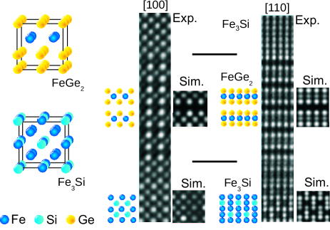
In Fig. 1, we can recognize the superstructure in the Ge-rich Ge(Fe,Si) film. The image of the [100] oriented sample shows brighter spots forming a square lattice. These spots are caused by Ge-columns (Z=32). The darker spots, which occur as center of every second square are due to Fe-columns (Z=26). In the image of the [110] oriented sample we see rows of brighter spots and can attribute them to Ge-columns. Between every second pair of bright rows we recognize darker spots and consider them as contrasts due to Fe-columns. In the Fe3Si film, we recognize the typical Fe-triplets of the image of the [110] oriented sample and the faint spots of the Si-columns between them (Z=14). The image of the [100] oriented sample shows a square lattice of relatively bright spots with darker spots in the centers of the squares. The DO3 structure of Fe3Si corresponding to this kind of contrast is known and can serve as a reference. On the basis of the Z-contrast of our HAADF micrographs obtained along the two crystal orientations [100] and [110], we are able to propose a structural model for the Ge(Fe,Si) film: It is the FeGe2 (P4mm) structure shown on the left side of Fig. 1. Four unit cells are depicted for better correspondence with the Fe3Si lattice. The structural models of Fe3Si (below, given as a reference) and FeGe2 (above, our proposal) are drawn. The experimental micrographs are compared to the structural models giving an illustration of our proposal of the FeGe2 structure. On the other hand, the well-known structure of the Fe3Si films is well reproduced, and so we can be sure that we described the FeGe2 structure in a good approximation.
The verification of the proposed FeGe2 structure (see Fig. 1) can be done using computer simulation of HAADF micrographs. We performed the simulations in the frozen phonon approximation using the parameters of the probe-Cs-corrected HR-STEM (JEOL ARM200) operating at 200 kV. Simulations and experimental micrographs shown in Fig. 1 agree well, indicating that a proper structural model was found. The location of the 5 at% Si detected by EDX spectroscopy is still unclear. The Si atoms probably are located on Ge sites. Besides, we found differently ordered regions of the Fe3Si, the B2 order located near the interface and the DO3 order in depth of the Fe3Si film.Hashimoto et al. (2007)
In Fig. 2 nano-beam diffraction patterns of the thin FeGe2 film from [100] and [110] oriented samples are given. The patterns were fully indexed using the proposed FeGe2 structure model and simulated in kinematical approximation. The results of the simulations given below in red color agree well with the experiments further supporting our structural model.
| EXP | PBE | HSE | |
|---|---|---|---|
| a(Fe3Si) | 0.5654 nm | 0.561 nm | 0.575 nm |
| 2a(FeGe2) | 0.5654 nm | 0.572 nm | 0.580 nm |
| c(FeGe2) | 0.5517 nm | 0.544 nm | 0.549 nm |
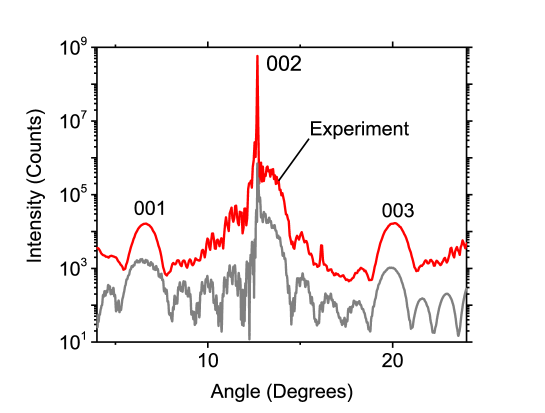
In Fig. 3, the XRD curve (symmetrical -scan, i.e. the 00L crystal truncation rod) together with the simulation of the diffraction curve of the Fe3Si/FeGe2/Fe3Si film stack in the vicinity of the GaAs(002) peak are shown. Here, the simulated diffraction curve agrees with the main features of the experimental diffraction curve, especially the FeGe2 001 and 003 maxima are visible, and the FeGe2 002 peak is shifted with respect to GaAs 002. In the supplemental material the XRD reciprocal space map of the non-symmetric 20L crystal truncation rod is shown.sup (2018) All relevant diffraction maxima of the reciprocal space map are positioned on a vertical line perpendicular to the sample surface, i.e. the structures are elastically strained and no plastic relaxation occurs.Heinke et al. (1994) From XRD we deduce the lateral lattice parameter of the epitaxial layer stack a = 0.5654 nm = 2 0.2827 nm and the strained vertical lattice parameter of the FeGe2 thin film of c = 0.5517 nm (cf. Table 1). A more careful analysis of the STEM HAADF micrographs allowed for determination of the strained lattice plane distances of two types of sublayers in the FeGe2 structure, viz. empty and filled ones. Empty layers and filled layers have distances of c1 = 0.266 nm and and c2 = 0.282 nm respectively. Filling with Fe leads to an expansion of the distance of the corresponding layer. This fact points to the possibility of strain compensation between the two sublayers of the FeGe2 lattice as a driving force for the formation of the ordered superlattice-like structure in the epitaxial layer stack.jen (2018) On the other hand, the integral layer thickness c1+c2 determined by STEM corresponds well to the strained c-value determined by XRD for the FeGe2 tetragonal lattice as a whole (see above). The theoretical values of the lattice parameters in Table 1 are given for unstrained lattices. In an epitaxial layer stack additional tetragonal deformation occurs.Hornstra and Bartels (1978); foo (2018)
Our results show that the ordering can be considered as a systematic arrangement of Fe-atoms and -vacancies in a CsCl-type FeGe lattice, where both atoms and vacancies are found on the Fe-sites, and the number of Fe-atoms is reduced by half in order to obtain the stoichiometry of FeGe2. A random positioning of the Fe-atoms would lead to a cubic lattice. But in our case we have the boundary condition at the FeGe2/Fe3Si interface, where the in-plane lattice parameter of FeGe2 is fixed to a value of 0.2827 nm. Let us take two CsCl-type unit cells to describe the FeGe2 lattice as a result of ordering of the Fe atoms and vacancies. Then the diffraction intensity of the fundamental 002 reflection is proportional to fFe + 2fGe, where fFe and fGe are the atomic form factors of the Fe-atom and the Ge-atom, respectively. The intensity of the 001 superlattice reflection is
| (4) |
because all other contributions vanish and only the ordered Fe-atoms give a diffraction signal. From the comparison of the intensities of the layer reflections 001 (superlattice) and 002 (fundamental) we obtain = (0.8050.02), i.e the ordering is nearly complete. The film consists of an almost ideal FeGe2 lattice. From the principle of minimum free energy the energy V lost by an atom moving from a disorder position to an order position can be calculated in the Gorsky-Bragg-Williams approximation.Gorsky (1928); Willliams (1935) This means in our case
| (5) |
For an order parameter = 0.805 and our annealing temperature of T = 513 K we obtain V= (0.0420.02) eV per atom.
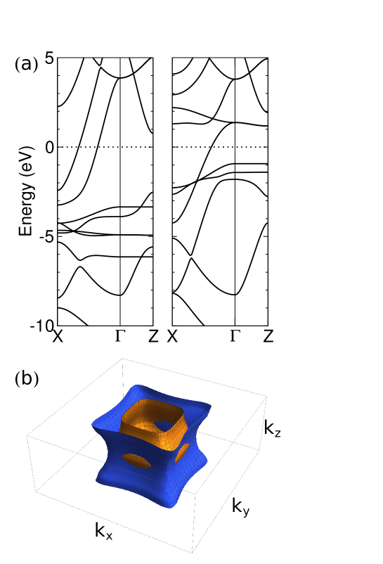
Thanks to the ordered structure of the FeGe2 film with the extended Fe-sheets we are expecting outstanding properties of the new material. As a first step, using the structural data of the FeGe2 obtained in the present work, we have calculated by DFT the band structure shown in Fig. 4(a). We can see, that the Fermi surfaces in Fig. 4(b) consist of cylinders along the z-axis, i.e. perpendicular to the Fe-sheets. The electrical properties in the plane of the Fe-sheets probably will differ considerably from those perpendicular to the sheets. FeGe2 belongs to a class of quasi-two-dimensional materials similar to MoS2.Rotjanapittayakul et al. (2018) Two-dimensional FeGe2 can now be fabricated with a thickness down to one nanometer, and high–TC superconductivity seems to be possible in such a structure.Stewart (2011); Miiller et al. (2015); Ge et al. (2015); Zhou et al. (2018) Thanks to the well ordered Fe-sheets, the concentration-waves can be accompanied by spin-density-waves.
Single crystal Ge-rich films were successfully grown by solid phase epitaxy on Fe3Si(001). Surprisingly the structure of the films was not the expected diamond structure of Ge, but a well oriented and layered tetragonal FeGe2 P4mm structure. A lattice misfit caused by interdiffusion of Si, Fe, and Ge leads to the formation of a new structure and ordering inside the film. We observe here one of the rare cases, where epitaxy is causing the formation of a distinct crystal structure differing from the equilibrium bulk structure, in particular the strain-induced ordering of the FeGe2 film with a periodicity along the direction perpendicular to the FeGe2/Fe3Si interface.
The authors thank Claudia Herrmann for her support during the MBE growth, Doreen Steffen, Margarita Matzek and Sabine Krauß for sample preparation, and Uwe Jahn for critical reading of the manuscript and helpful discussion. This work was supported in part by the Office of Naval Research through the Naval Research Laboratorys Basic Research Program. Some computations were performed at the DoD Major Shared Resource Center at AFRL. We thank the Helmholtz-Zentrum Berlin (HZB) for providing beamtime at the BESSY-beamline U125/2 KMC with the endstation PHARAO.
References
- Kuan et al. (1985) T. S. Kuan, T. F. Kuech, W. I. Wang, and E. L. Wilkie, Phys. Rev. Lett. 54, 201 (1985).
- Ourmazd and Bean (1985) A. Ourmazd and J. C. Bean, Phys. Rev. Lett. 55, 765 (1985).
- Martins and Zunger (1986) J. L. Martins and A. Zunger, Phys. Rev. Lett. 56, 1400 (1986).
- Mbaye et al. (1987) A. A. Mbaye, L. G. Ferreira, and A. Zunger, Phys. Rev. Lett. 58, 49 (1987).
- Gorsky (1928) W. Gorsky, Z. Phys. 50, 64 (1928).
- Willliams (1935) E. J. Willliams, Proc. Roy. Soc. A 152, 231 (1935).
- Khachaturyan (1973) A. G. Khachaturyan, Phys. Stat. Sol. B 60, 9 (1973).
- Khachaturyan (1983) A. G. Khachaturyan, Theory of Structural Transformations in Solids (John Wiley and Sons, Inc., New York, 1983).
- Ruban and Abrikosov (2008) A. V. Ruban and I. A. Abrikosov, Rep. Prog. Phys. 71, 046501 (2008).
- Zhuravlev et al. (2014) I. A. Zhuravlev, J. M. An, and K. D. Belashchenko, Phys. Rev. B 90, 214108 (2014).
- Wr´obel et al. (2015) J. S. Wr´obel, D. Nguyen-Manh, M. Y. Lavrentiev, M. Muzyk, and S. L. Dudarev, Phys. Rev. B 91, 024108 (2015).
- Tinkham et al. (2008) B. P. Tinkham, B. Jenichen, V. M. Kaganer, R. Shayduk, W. Braun, and K. H. Ploog, J. Cryst. Growth 310, 3416 (2008).
- Jenichen et al. (2009) B. Jenichen, V. M. Kaganer, R. Shayduk, W. Braun, and A. Trampert, Phys. Stat. Sol. A 206, 1740 (2009).
- Jenichen et al. (2005) B. Jenichen, V. M. Kaganer, J. Herfort, D. K. Satapathy, H.-P. Schonherr, W. Braun, and K. H. Ploog, Phys. Rev. B 72, 075329 (2005).
- Yamada et al. (2012) S. Yamada, K. Tanikawa, M. Miyao, and K. Hamaya, Crystal Growth and Design 12, 4703 (2012).
- Jenichen et al. (2014) B. Jenichen, J. Herfort, U. Jahn, A. Trampert, and H. Riechert, Thin Solid Films 556, 120 (2014).
- Kawano et al. (2016) M. Kawano, M. Ikawa, K. Arima, S. Yamada, T. Kanashima, and K. Hamaya, J. Appl. Phys. 119, 045302 (2016).
- Gaucher et al. (2017) S. Gaucher, B. Jenichen, J. Kalt, U. Jahn, A. Trampert, and J. Herfort, Appl. Phys. Lett. 110, 102103 (2017).
- Sakai et al. (2017) S. Sakai, M. Kawano, M. Ikawa, H. Sato, S. Yamada, and K. Hamaya, Semicond. Sci. Technol. 320, 094005 (2017).
- Kawano et al. (2017) M. Kawano, M. Ikawa, K. Santo, S. Sakai, H. Sato, S. Yamada, and K. Hamaya, Phys. Rev. Materials 1, 034604 (2017).
- Hamaya et al. (2013) K. Hamaya, Y. Baba, G. Takemoto, K. Kasahara, S. Yamada, K. Sawano, and M. Miyao, J. Appl. Phys. 113, 183713 (2013).
- Wu (2005) K. Wu, US Patent , 6963121B2 (2005).
- Yuasa and Djayaprawira (2007) S. Yuasa and D. D. Djayaprawira, J. Phys. D: Appl. Phys. 40, R337 (2007).
- Oogane and Mizukami (2011) M. Oogane and S. Mizukami, Phil. Trans. R. Soc. A 369, 3037 (2011).
- sup (2018) Supplemental material which includes a more detailed description of the TEM and XRD experiments as well as the results of energy dispersive X-ray (EDX) spectroscopy, HAADF original data, and XRD reciprocal space mapping (2018).
- Stadelmann (2016) P. Stadelmann, Electron Microscopy Simulation JEMS (http://www.jems-saas.ch/, Lausanne, 2016).
- CrystalMaker (2017) CrystalMaker, software for interactive crystal/molecular structures: modelling and diffraction by CrystalMaker Software Limited, http://www.crystalmaker.com/ (2017).
- Stepanov (1997) S. A. Stepanov, Collection of x-ray software (http://sergey.gmca.aps.anl.gov/ , Chicago, 1997).
- Perdew et al. (1996a) J. P. Perdew, K. Burke, and M. Ernzerhof, Phys. Rev. Lett. 77, 3865 (1996a).
- Kresse and Furthmuller (1996) G. Kresse and J. Furthmuller, Phys. Rev. B 54, 11169 (1996).
- Kresse and Furthmueller (1996) G. Kresse and J. Furthmueller, Comput. Mater. Sci. 6, 15 (1996).
- Perdew et al. (1996b) J. P. Perdew, M. Ernzerhof, and K. Burke, J. Chem. Phys. 105, 9982 (1996b).
- Heyd et al. (2003) J. Heyd, G. E. Scuseria, and M. Ernzerhof, J. Chem. Phys. 118, 8207 (2003).
- Herfort et al. (2006) J. Herfort, A. Trampert, and K. H. Ploog, Int. J. Mat. Res. 97, 1026 (2006).
- foo (2018) The Si content of 5 atom percent can lead in principle to a lattice contraction of about 0.4 percent. We neglect this in the present work, because we do not know the position of the Si atoms in the lattice. (2018).
- Jaafar et al. (2010) R. Jaafar, D. Berling, D. Sbilleau, and G. Garreau, Phys. Rev. B 81, 155423 (2010).
- Satyamurthy et al. (1965) N. S. Satyamurthy, R. J. Begum, C. S. Somanathan, and M. R. Murthy, Sol. State Com. 3, 113 (1965).
- Pennycook and Jesson (1990) S. J. Pennycook and D. E. Jesson, Phys. Rev. Lett. 64, 938 (1990).
- VanAert et al. (2011) S. VanAert, K. J. Batenburg, M. D. Rossel, R. Erni, and G. VanTendeloo, Nature 470, 374 (2011).
- Zuo et al. (2014) J.-M. Zuo, A. Shah, H. Kim, Y. Meng, W. Gao, and J.-L. Rouviére, Ultramicroscopy 136, 50 (2014).
- Hashimoto et al. (2007) M. Hashimoto, A. Trampert, J. Herfort, and K. H. Ploog, J. Vac. Sci. Technol. B 25, 1453 (2007).
- Heinke et al. (1994) H. Heinke, M. O. Möller, D. Hommel, and G. Landwehr, J. Cryst. Growth 135, 41 (1994).
- jen (2018) DFT yielded the lattice parameters of first a hypothetical primitive Ge lattice: a = 0.268 nm (a = 0.272 nm) and second a hypothetical CsCl-type GeFe lattice: a = 0.288 nm (a = 0.290 nm) correspondingly for HSE(PBE) functional. The halved lattice-parameter a/2 of Fe3Si of 0.2827 nm lies between those values of the DFT calculations for the hypothetical primitive and the CsCl-type lattices, so that a strain compensation between the two parts of the Ge2Fe lattice seems possible (2018).
- Hornstra and Bartels (1978) J. Hornstra and W. J. Bartels, J. Cryst. Growth 44, 513 (1978).
- Rotjanapittayakul et al. (2018) W. Rotjanapittayakul, W. Pijitrojana, T. Archer, S. Sanvito, and J. Prasongkit, Sci. Rep. 8, 4779 (2018).
- Stewart (2011) G. R. Stewart, Rev. Mod. Phys. 83, 1589 (2011).
- Miiller et al. (2015) W. Miiller, J. M. Tomczak, J. W. Simonson, G. Smith, G. Kotliar, and M. C. Aronson, J. Phys.: Condens. Matter 27, 175601 (2015).
- Ge et al. (2015) J.-F. Ge, Z.-L. Liu, C. Liu, C.-L. Gao, D. Qian, Q.-K. Xue, Y. Liu, and J.-F. Jia, Nature Mat. 14, 285 (2015).
- Zhou et al. (2018) Y. Zhou, L. Miao, P. Wang, F. F. Zhu, W. X. Jiang, S. W. Jiang, Y. Zhang, B. Lei, X. H. Chen, H. F. Ding, H. Zheng, W. T. Zhang, J. F. Jia, D. Qian, and D. Wu, Phys. Rev Lett. 120, 097001 (2018).