Anomalous anisotropic behaviour of spin-triplet proximity effect in Au/SrRuO3/Sr2RuO4 junctions
Abstract
Spin-polarized supercurrents can be generated with magnetic inhomogeneity at a ferromagnet/spin-singlet-superconductor interface. In such systems, complex magnetic inhomogeneity makes it difficult to functionalise the spin-polarized supercurrents. However, spin-polarized supercurrents in ferromagnet/spin-triplet-superconductor junctions can be controlled by angle between magnetization and spin of Copper pairs (-vector), that can effectively be utilized in developing of a field of research known as superconducting spintronics. Recently, we found induction of spin-triplet correlation into a ferromagnet SrRuO3 epitaxially deposited on a spin-triplet superconductor Sr2RuO4, without any electronic spin-flip scattering. Here, we present systematic magnetic field dependence of the proximity effect in Au/SrRuO3/ Sr2RuO4 junctions. It is found that induced triplet correlations exhibit strong anisotropic field response. Such behaviour attributes to the rotation of the -vector of Sr2RuO4. This anisotropic behaviour is in contrast with the vortex dynamic. Our results will stimulate study of interaction between ferromagnetism and unconventional superconductivity.
1 Introduction
Generation of dissipationless spin-polarized (spin-triplet) supercurrent is the major interest of superconducting devices, which can be utilized to establish energy efficient superconducting spintronics [1, 2]. In last two decades, rigorous works have been conducted to produce and control spin-triplet supercurrents using heterostructures of ferromagnets (Fs) and conventional spin-singlet superconductors (SSCs) [3, 5, 4, 6, 7, 8, 9, 10, 11, 12, 13]. It has been established that magnetic inhomogeneity is always required to emerge spin-triplet supercurrent at F/SSC interface, which can be achieved by using non-collinear magnetization in multilayer ferromagnets [6, 7, 9]. Complicated magnetic structure of multilayer ferromagnets makes it hard to functionalize the F/SSC devices. It can be settled by replacing SSC with a spin-triplet superconductor (TSC). In F/TSC heterostructures, a single F layer can affectively emerge spin-polarized supercurrents with fully conserved spin degree of freedom in the entire device. Furthermore, recent theoretical work suggested that superconducting properties of F/TSC junctions strongly depends on relative orientation of magnetization () of a F and -vector of a TSC [14, 15, 16, 17, 18]. Interestingly, when the -vector and are perpnadicular (angle between -vector and ) the spin-triplet correlation can be induced monotonically over a long range. However, for parallel configuration, , the induced order parameter oscillates spatially [18].
Sr2RuO4 (SRO214) is one of the best-candidates of TSCs [19] with the superconducting critical temperature () of 1.5 K. Most likely, it exhibits the chiral -wave spin-triplet state with broken time-reversal symmetry [20, 21, 22, 23, 24, 25, 26, 27, 28], although there are still unresolved issues [29, 30, 31]. Very recent nuclear magnetic resonance (NMR) study shows the reduction of Knight shift, which cannot be explained by spin-striplet scenario[32, 33]. Recently, SRO214 attracts interest for exploring topological superconducting phenomena originating from its orbital phase winding [26, 19, 27, 28]. The superconducting order parameter of a SRO214 (TSC) can be represented by a vector , where is the out-of-plane (along the -axis) basis vector, and and are the and components of the orbital order parameters, respectively [19]. Note that the -vector is always perpendicular to the spin of triplet Cooper pairs. For bulk SRO214 superconductor -vector is aligned along the -axis (out-of-plane) fixed by spin-orbit coupling [34, 35, 36] but at the surface it may not be true because of surface effects. It is expected that -vector may rotate to the in-plane direction with external magnetic field of about 20 mT applied along the out-of-plane direction [37, 38].
Newly, we developed F/TSC heterostructures by growing epitaxial ferromagnetic SrRuO3 (SRO113) thin films on a spin-triplet superconductor SRO214 single crystal using pulsed laser deposition [39]. Furthermore, long-ranged proximity effect is also observed, where even frequency -wave spin-triplet may dominate compared to odd frequency -wave spin-triplet, as junctions were in clean limit [40, 41].
In this article, we present our investigations on differential conductance (/) of Au/SRO113/SRO214 junctions as a function of temperature and magnetic field applied along both in-plane () and out-of-plane () directions. We found that the induced correlation exhibits anisotropic behavior in the response of applied field. Vortex dynamics cannot explain our results. This anisotropic effect can be attributed to the relative orientation of the -vector of SRO214 and of SRO113.
2 Results
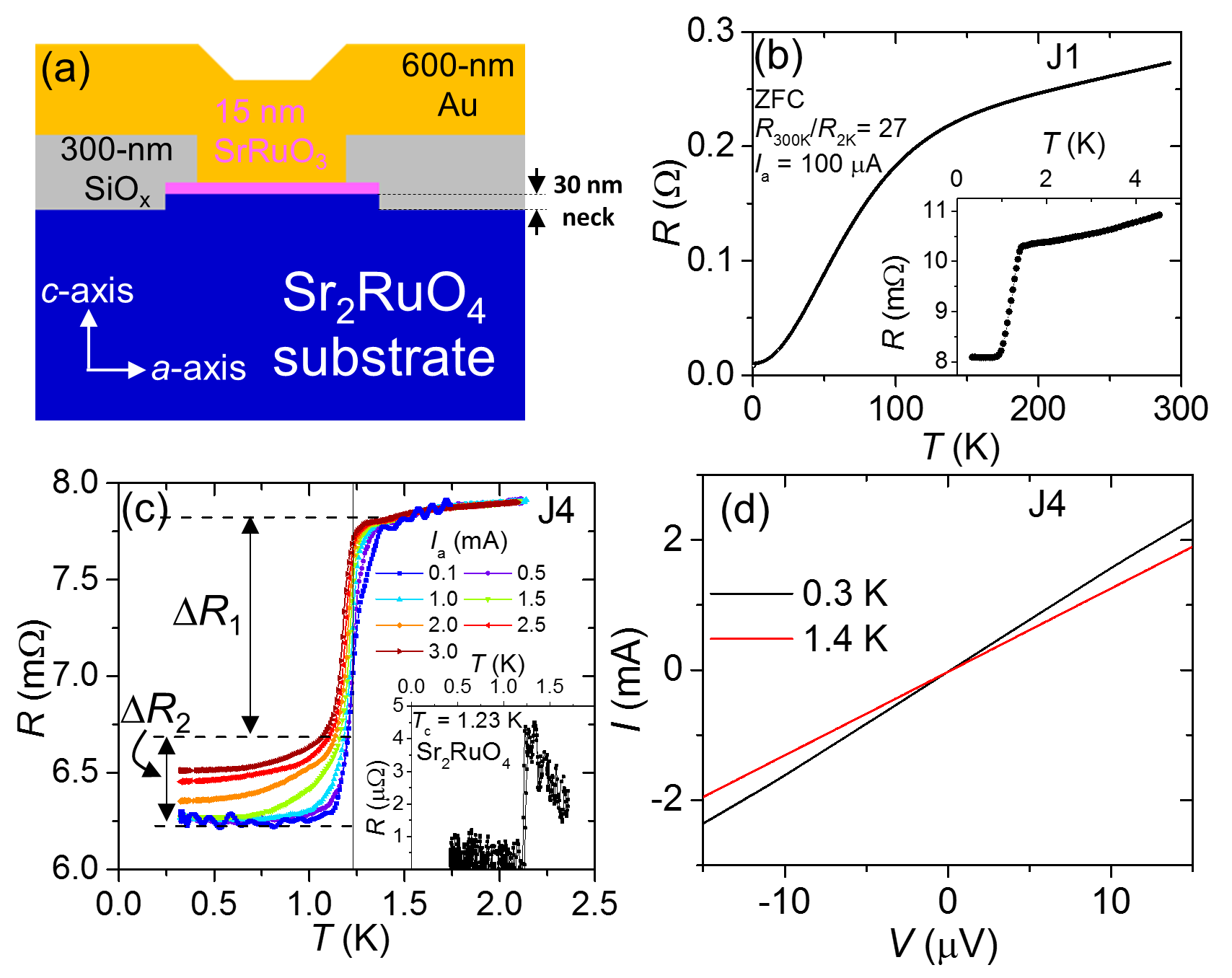
In this article, we present the results of various junctions but mainly focused on two junctions J4 and J5 that exhibit different normal-state resistance () 7.83 m and 198 m, respectively. A schematic illustration of a junction is shown in the Fig. 1(a).
Temperature dependent resistance () was measured during cooling in zero field down to 300 mK. SRO214, SRO113 and Au are good metals with very low resistivity at low temperatures, except the resistivity of SRO214 along the -axis () [29]. It suggests that at low temperatures resistivity of our junctions is dominated by the SRO113/SRO214 and Au/SRO113 interfaces [39, 40]. Our present junctions exhibit RRR = 27 that is three times larger than that of our previous junctions [40]. Furthermore, a sharp superconducting transition is observed that reflects good quality of the junctions (inset of Fig. 1(b)). It is also clear that in the normal state, the resistivity data have major contributions of of SRO214. It indicates that current is flowing along the normal of the junctions, which excludes the possibility of any direct contact between Au electrode and SRO214 superconductor.
Figure 1(c) presents () at low temperatures of Junction J4 (5 5 m2) measured with different applied currents ( in the range of 0.1 to 3 mA) that shows two superconducting regions robust and weak against . At = 0.1 mA the transition onset appears at 1.38 K, which is higher than the 1.23 K of SRO214 substrate (see the inset of Fig. 1(c)). This increase in may arises due to mutual strain (pressure) between the substrate and the film close to the interface [42]. The () behavior with increasing reveals that there are two distinct transition regions. The first transition with change in the resistance 1.15 m is only weakly dependent on . The second transition is strongly suppressed with increasing with the change in the resistance of 0.45 m. Multiple transitions are expected to emerge in a multi-barrier junction such as the junctions presented here: Normal-metal/F/TSC. Essentially, the same behaviour has been observed in our previous study [40]. These observations suggest that and correspond to SRO113/SRO214 and Au/SRO113 interfaces, respectively. It means that the / as a function of bias voltage should exhibit Andreev reflection (AR) features occurring at two distinct interfaces. Note that AR can occur for a bias voltage below superconducting gap (induced minigap in SRO113 [41]) at SRO113/SRO214 (Au/SRO113) interface. To study the AR, we obtained /() by taking first order numerical derivative of the measured current-voltage (-) curves shown in Fig. 1(d). We investigate the / as a function of externally applied magnetic fields both in-plane and directions and temperature as well.
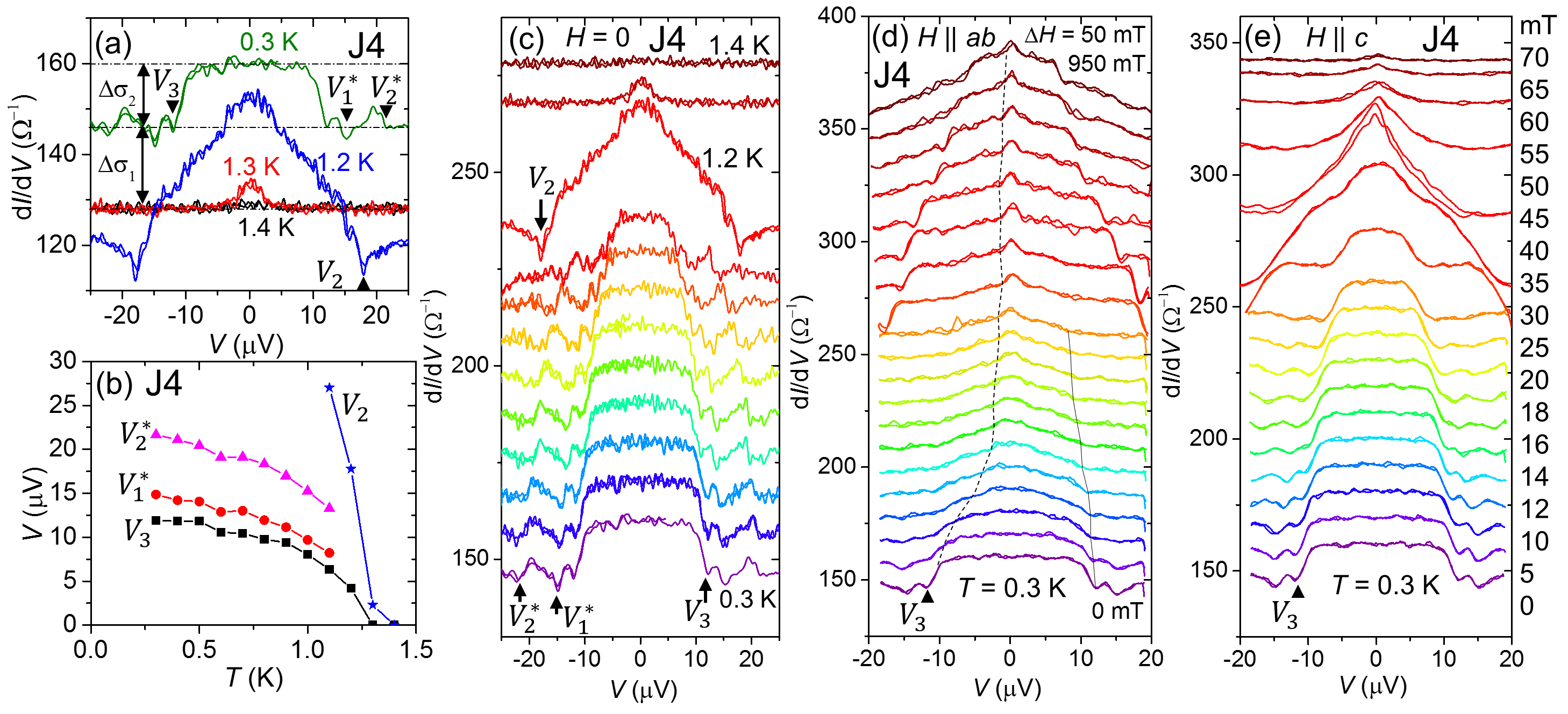
First, we present / data measured at different temperatures (see Fig. 2(a)). It shows an enhancement in / below superconducting transition temperature . Below , the conductance of a transparent F/SSC interface increases with opening of AR channel, which is related with spin-polarization of the ferromagnet as well. At 0.3 K and zero applied field (after zero field cooling), the conductance enhances by 10 below with almost flat top. This transition yields the change in the conductance 13.84 that corresponds to (second transition in ()). At temperatures higher than 1.1 K an additional enhancement within our applied bias voltage can be observed at . Note that there are sharp dips associated with features (Fig. 2(a)), which may correspond to the destruction of superconductivity at SRO113/SRO214 interface with critical current[41]. However, the temperature dependence of / (Fig. 2(c)) shows that the dip persists up to the bulk , which suggests that the dip can be attributed to the critical current of SRO214-neck part of the junctions, and the proximity effect at the SRO113/SRO214 interface is simultaneously switched off. The transition exhibits 14 increase with 18.04 consistent with (first transition in ()). It indicates that characteristic voltages of and are corresponding to multi AR features occurred at Au/SRO113 and SRO113/SRO214 interfaces, respectively. The data presented in Fig. 2(b)) is extracted from Fig. 2(c). It shows a monotonic suppression of the AR with increase in the temperature. Similar behaviour is observed for junction J5 as well which is shown in Fig. 3(f) and discussed more at the end of the section.
The observations of multiple enhancements in / reveal that superconductivity penetrates into a 15-nm thick SRO113 layer and reaches at Au/SRO113 interface as well, which is only possible with spin-triplet superconducting correlation, since spin-singlet coherence length of SRO113 is on the order of 1-nm [43]. Note that two additional oscillations with minima at and appear between and . These oscillations are suppressed monotonically just like with the increase in the temperature, see Fig. 2(b) and (c). These oscillations may correspond to McMillan-Rowell resonance [44] resulting from interference between Andreev reflected quasiparticles at the SRO113/SRO214 interface and the quasiparticles reflected back into SRO113-layer from the Au/SRO113 interface.
The most interesting and important part of this study is voltage biased / as a function of applied field. Figures 2(d) and (e) shows the /() data obtained with the fields and , respectively. In case of the applied field , is abruptly suppressed up to 200 mT and decreases slowly with further increase in . In contrast is suppressed gradually, which is an expected behaviour of Cooper pair breaking under applied magnetic fields (orbital effects). For fields , both and decreases monotonically. Thus spin-triplet proximity effect into the SRO113 layer exhibits an anisotropic response to applied field. Such an effect can be expected for anisotropic -vector rotation with applied field, further discussions are given in the discussions section.
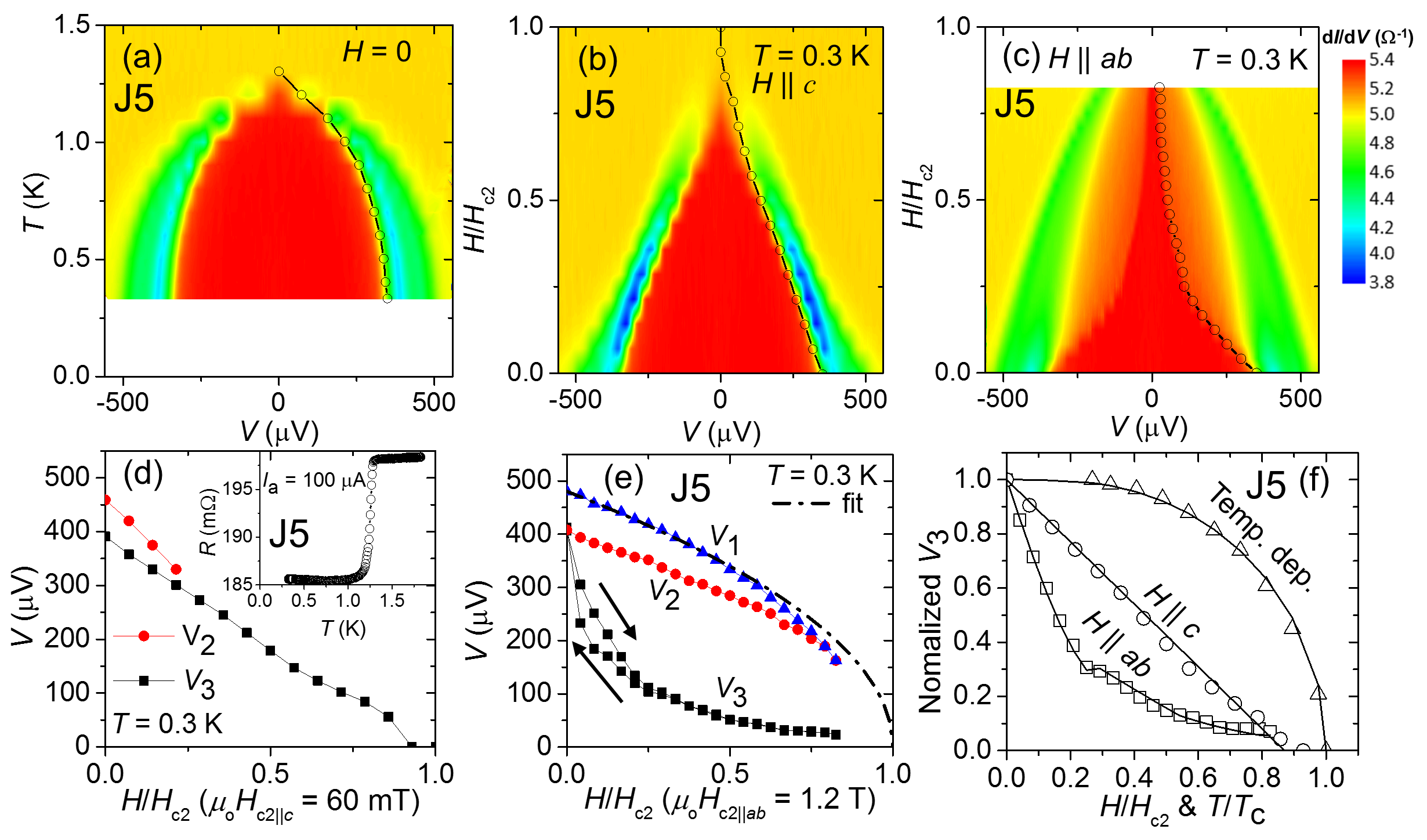
Junction J4 with lower exhibits various interesting features in the junction voltage. However, concerning to the signal to noise ratio a junction with larger is preferable. Indeed in Junction J5 with rather high 198.2 m, we observed good quality data that also exhibits AR features with multiple transitions. For Junction J5, /() as a function of temperature and applied field exhibit two transitions corresponding to and . Note that we also obtained the feature particularly at 0.3 K and zero field as observed in our previous junctions [40]. The characteristic voltage most probably arises due to critical-current of SRO214 neck [40]. Note; in this junction the oscillations corresponding to McMillan-Rowell resonance are not observed due to its lower amplitude and higher . By comparing Figs. 3(b) and (c), a strong anisotropy in is obviously reproduced. In fact, we observed this anisotropic effect in almost all our working junctions.
For Junction J5, under the effect of fields, the characteristic voltage shown in blue Fig. 3(b) becomes vague at higher fields as shown in Fig. 3(d). It reflects that in junctions with higher (lower interface conductance) the AR features are overlapped with each other. However, all the characteristic-voltage features are obviously present for all fields, see Fig. 3(e). Interestingly, exhibits hysteretic effect only below 200 mT. For a comparison, we plotted normalized as a function of field and temperature in Fig. 3(f).
We applied theoretical fits on temperature and field dependent to analyse its behavior. The behaviour of versus temperature follows the interpolation formula, with constant , which is relatively lower than the expected value of 1.74 for s-wave conventional BCS superconductivity. Interesting, a=1.56 is indicating unconventional superconducting proximity effect and potentially consistent with -wave superconductivity [45, 41]. The monotonic suppression of under fields can be reasonably fitted with the expression . However, under fields is strongly suppressed at lower fields less than 200 mT and slowly decreases for higher fields. Note that the coercive field of SRO113 layer is 200 mT for rectangular pads of the size of tens of microns [40]. It indicates that there are two distinct decoherence effects on the induced spin-triplet correlation in the SRO113 layer, such as orbital effect and rotation relative to the -vector of SRO214 superconductor. The phenomenological fit shown in Fig. 3(f) is discussed below.
3 Discussion
Before starting our discussion, let us summarize our main results. We observed AR features in / with characteristic voltages and emerged at Au/SRO113 and SRO113/SRO214 interfaces, respectively. The () exhibits anisotropic (isotropic) behaviour in the response of applied magnetic field. The AR feature with is suppressed strongly below 200 mT and decreases slowly with farther increase under the field . However, decreases monotonically with and as well. For the field along the -axis decreases similar to .
First, we discuss the subtraction of resistance contributions other than interfaces to estimate the accurate values of characteristic voltages and . As described below, the measured resistance of our devices may contain some contributions from non-interface resistance, such as from the neck part of SRO214. To estimate accurate values of characteristic voltages specifically, at 0.3 K, we subtract the contributions of estimated additional resistances. For simplicity, let us assume an ideal situation that AR probability is 100 so that the conductance of each interface is enhanced by a factor of two compared to its normal-state conductance. Under this assumption, for Junction-J4 (Junction-J5) the total resistance of Au/SRO113 and SRO113/SRO214 interface is two times the m (12.74 m). At 0.3 K, additional resistance of Junction-J4 (Junction-J5) 4.73 m (172.72 m) that contributes additional voltage drop across the junction. We subtract a linear contribution of and plotted the results in Fig. 4(a). It reveals that for junction-J4 (junction-J5) is 3 V ( 20 V). It shows that junction-J5 exhibits an order higher due to lower interface transparency and more drop of voltage across it.
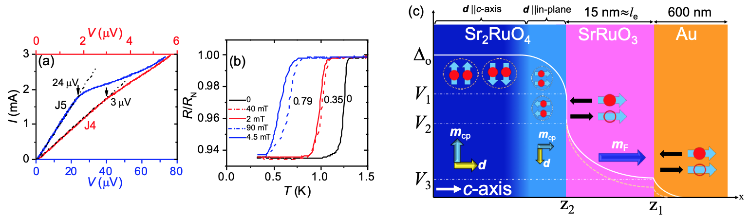
It is important to discuss the vortex effect on proximity effect in Au/SRO113/SRO214 junctions, which can also be anisotropic. Of course, vortices can be induced for the fields higher than . Note that of SRO214 is 1 mT and 70 mT along the -axis (in-plane) and the -axis[19], respectively. Transport properties of a superconducting junction can be affected when vortices are crossing the interface because of vortex dynamics. According to the geometry of our junctions (-axis is out-of-plane normal of the junction), the field induced vortices can encounter the interface only for fields . However, vortices align parallel to the interface for the fields . It means, AR features should exhibit additional suppression for fields . In contrast, is suppressed strongly for the fields only.
To understand the effect of vortices in our junctions, we measured () under the fields and . The of first transition with of SRO113/SRO214 interface decreases more for same effective field applied along the -axis compared for the in-plane direction, see Fig. 4(b). However, second transition corresponding to Au/SRO113 interface is in contrast. It indicates that the electronic transport properties of our junctions can encounter vortices only for the fields . Furthermore, it also reveals that the observed anisotropic response of under applied fields does not arise due to vortex dynamics.
Effect from the spin part: spin-triplet proximity effect at F/TSC interface can be dictated by angle between -vector of SRO214 and vector of SRO113 layer [14, 15, 16, 17, 18]. We applied a following phenomenological fit to (),
| (1) |
Where, (0) is the characteristic voltage at zero temperature, and cos() with a constant . We obtained a good fit by changing the nonmonotonically; first decreased until 200 mT and increased for higher fields. Furthermore, we presumed that -vector is aligned along the in-plane direction at the interface.
In bulk SRO214 superconductor, the -vector is aligned along the -axis and in the result the spins of the Cooper pairs are aligned along the -plane. Thus, the -vector and Cooper pair spins can be rotated with an applied magnetic field of 20 mT [37, 38] to in-plane and to out-of-plane, respectively. In this scenario, cannot rotate the -vector. That means, proximity effect should supress more in case of rather than . But, our results are suggesting in contrast.
If the -vector is perpendicularto the -axis particularly at the interface, can be affected with rotation of with . It can be possible that broken inversion symmetry at the SRO113/SRO214 interface induces Rashba-type [46] spin-orbit coupling with in-plane vector characterizing the spin–orbit coupling with out-of-plane effective field, which tends to align the -vector along the in-plane direction. Additionally, out-of-plane magnetic anisotropy of SRO113 thin film is also supporting such an alignment of the -vector. In the result, at zero applied field, spin of triplet Cooper pairs in SRO214 and of SRO113 are parallel and in the result , which is a favourable configuration for proximity effect in F/TSC junctions. The angle can be reduced with either rotation of or -vector that dictates the proximity effect in the junction accordingly [18]. It is most likely that the rotation of of SRO113 is responsible for first strong suppression in up to coercive field of SRO113-layer 200 mT [40]. It may also be the reason of hysteresis in below 200 mT; above 200 mT, is saturated and fully aligned along the . In the results decreases up to coercive field and suppresses the proximity effect. On the other hand, at the same time, the applied field tends to align the -vector along the -axis. Therefore, never becomes zero and proximity effect is weakly suppressing with increasing above 200 mT. In this configuration of -vector at the interface as illustrated in Fig. 4(c), the cannot rotate the -vector, as spins of Cooper pairs are aligned out-of-plane. Therefore, the suppresses monotonically with . Of course, temperature change between 2 K and 0.3 K cannot change or -vector, thus, there is no anomalous suppression in as a function of temperature.
The rotation of the -vector under the influence of an external magnetic field is well known for superfluid 3He-A phase [48] analogous to chiral -wave spin-triplet superconductivity anticipated in SRO214. In case of the standard chiral--wave scenario for SRO214, the -vector should be fixed along the -axis because of spin-orbit coupling. Possibility of rotation of the -vector to an in-plane direction under -axis magnetic field is discussed in the NMR study for [37]. However, at SRO113/SRO214 interface, broken inversion symmetry and out-of-plane exchange field of SRO113 can significantly affect the spin-orbit coupling. That may result into easier rotation of the -vector along the in-plane direction. This scenario explains our results well. Theoretically, Annett et al., [38] predicted that the -vector rotation by magnetic field along the -axis is accompanied by chiral to nonchiral phase transition depending on spin dependent effective pairing interaction. However, for a proximity effect in a junction based on a spin-triplet superconductor, the crucial parameter is the orientation of the -vector [18], whereas, the transition in the orbital part may not considerably modulate the proximity effect unless the junction size is of the order of the typical size of a chiral domain.
Effect from the orbital part: SRO214 exhibits multi-component () superconducting order parameter [28]. That may also explain this anisotropic behaviour of . The component can be significantly suppressed compared to the when magnetic field is parallel to and vice versa [49, 50, 51]. However, the fields along -direction, perpendicular to the both and components, can simultaneously affect both components of the order parameter. In this way, the differential conductance should depend differently on the in-plane and out-of-plane applied magnetic fields. Such anisotropic effect corresponding to the order parameter of the bulk SRO214 should emerge mainly in the SRO214 side and that should result in anisotropic behaviour either only in or both and . Thus, our observed anomalous anisotropic behaviour only in cannot be explained by the above mentioned non-chiral scenario. Rather, this observation supports that the spin-triplet proximity effect is controlled with the change in due to the relative rotation of m and d-vector. More experimental and theoretical works are needed to understand and manipulate the rotation of .
4 Conclusion
We studied long-range proximity effect in Au/SRO113/SRO214 double barrier junctions. Two distinct Andreev reflection features are observed in differential conduction vs bias voltage coming from two SRO113/SRO214 and Au/SRO113 interfaces with the induction of spin-triplet Cooper pairs in 15-nm thick SRO113 from SRO214. The transition of Au/SRO113 interface is suppressed anisotropically with externally applied magnetic fields. This anomalous anisotropic behaviour cannot be explained with vortex dynamics since differential conductance as a function of temperature and out-of-plane applied fields if qualitatively similar. However, conductance of SRO113/SRO214 interface suppressed faster when field is applied along the in-plane direction. Our results will stimulate the theoretical work to understand the correlation between unconventional superconductivity and ferromagnetism, -wave proximity effect and applications to initiate the Superconducting Spintronics.
Methods
Single crystals of SRO214 were grown in Kyoto using a floating-zone method [47]. Some parts of the SRO214 crystals tend to contain Sr3Ru2O7, SRO113, as well as Ru-metal inclusions. These inclusions are unavoidable in order to eliminate Ru deficiencies and obtain close to the intrinsic 1.5 K. To fabricate our superconducting junctions, we carefully choose the parts of SRO214 crystals that do not contain impurities but with a slightly lower 1.23 K. Ferromagnetic SRO113 thin films with thickness of 15-nm were epitaxially deposited using pulsed laser deposition on the cleaved -surface of the SRO214 substrates (3 3 0.5 mm3) in Seoul. The details of SRO113 thin film deposition can be found elsewhere [39, 40]. Immediately after the growth of SRO113 film, a 5-nm thick Ti adhesive layer and a 20-nm thick Au capping layer were deposited ex-situ by dc-sputtering.
Double interface Au/SRO113/SRO214 junctions shown schematically in Fig. 1a were fabricated in RIKEN. First, 25 25 m2 and 10 10 m2 pads of SRO113 were prepared on flat surfaces using photolithography and Ar ion etching. Then, an insulating 300-nm thick SiOx layer was sputtered. Finally, a 600-nm thick Au top electrode was deposited by electron beam evaporation with junction areas of 20 20 m2 and 5 5 m2 over 25 25 m2 and 10 10 m2 SRO113 pads, respectively. Note, a 30-nm thick neck part of SRO214 substrate was prepared with over-etching during SRO113 layer etching to define a bottom superconducting electrode, as shown in Fig. 1(a). Detailed descriptions of these processes are given in Ref. [40].
Electrical transport measurements were performed using the four-point technique with two contacts (, ) on the Au top electrode and the other two contacts (, ) connected directly to the side of the SRO214 crystal. Transport properties were studied down to 300 mK using a 3He cryostat equipped with a vector superconducting magnet.
References
- [1] Eschrig, M., Spin-polarized supercurrents for spintronics: a review of current progress. Rep. Prog. Phys. 78, 104501 (2015).
- [2] Linder, J. and Robinson, J. W. A., Superconducting spintronics. Nat. Phys. 11, 307 (2015).
- [3] Bergeret, F. S., Volkov, A. F. and Efetov, K. B., Long-range proximity effects in superconductor-ferromagnet structures. Phys. Rev. Lett. 86, 4096 (2001).
- [4] Eschrig, M. and Löfwander, T., Triplet supercurrents in clean and disordered half-metallic ferromagnets. Nat. Phys. 4, 138 (2008).
- [5] Keizer, R. S., Goennenwein, S. T. B., Klapwijk, T. M., Miao, M., Xiao, G. and Gupta, G., A spin triplet supercurrent through the half-metallic ferromagnet CrO2. Nature(London) 439, 825 (2006).
- [6] Khaire, T. S. , Khasawneh, M. A., Pratt, Jr. W. P. and Birge, N. O., Observation of spin-triplet superconductivity in Co-based Josephson junctions. Phys. Rev. Lett. 104, 137002 (2010).
- [7] Robinson, J. W. A., Witt, J. D. S. and Blamire, M. G., Controlled injection of spin-triplet supercurrents into a strong ferromagnet. Science 329, 59 (2010).
- [8] Anwar, M. S., Czeschka, F., Hesselberth, M. Porcu, M. and Aarts, J., Long-range supercurrents through half-metallic ferromagnetic CrO2. Phys. Rev. B 82, 100501(R) (2010).
- [9] Anwar, M. S., Veldhorst, M., Brinkman, A. and Aarts, J., Long range supercurrents in ferromagnetic CrO2 using a multilayer contact structure. Appl. Phys. Lett. 100, 052602 (2012).
- [10] Bergeret F. S. and Tokatly, I. V., Singlet-Triplet Conversion and the Long-Range Proximity Effect in Superconductor-Ferromagnet Structures with Generic Spin Dependent Fields. Phys. Rev. Lett. 110, 117003 (2013).
- [11] Bergeret F. S. and Tokatly, I. V., Spin-orbit coupling as a source of long-range triplet proximity effect in superconductor-ferromagnet hybrid structures. Phys. Rev. B 89, 134517 (2014).
- [12] Jacobsen, S. H., Kulagina, I. and Linder, J., Controlling superconducting spin flow with spin-flip immunity using a single homogeneous ferromagnet. Sci. Rep. 6, 23926 (2016).
- [13] Banerjee, N., Ouassou, J. A., Zhu, Y., Stelmashenko, N. A., Linder, J. and Blamire, M. G., Controlling the superconducting transition by spin-orbit coupling. Phys. Rev. B 97, 184521 (2018).
- [14] Brydon, P. M. R. and Manske, D., Transition in Magnetic Triplet Superconductor Josephson Junctions. Phys. Rev. Lett. 103, 147001 (2009).
- [15] Brydon, P. M. R., Spontaneous spin current due to triplet superconductor-ferromagnet interfaces. Phys. Rev. B 80, 224520 (2009).
- [16] Annunziata, G., Cuoco, M., Noce, C., Sudbø, A. and Linder, J., Spin-sensitive long-range proximity effect in ferromagnet/spin-triplet-superconductor bilayers. Phys. Rev. B 83, 060508(R) (2011).
- [17] Gentile,P., Cuoco, M., Romano, A., Noce, C., Manske, D. and Brydon, P. M. R., Spin-orbital coupling in a triplet superconductor-ferromagnet junction. Phys. Rev. Lett. 111, 097003 (2013).
- [18] Terrade, D., Gentile, P., Cuoco, M. and Manske, D., Proximity effects in a spin-triplet superconductor–ferromagnet heterostucture with a spin-active interface. Phys. Rev. B 88, 054516 (2013).
- [19] Maeno, Y, Kittaka, S., Nomura, T., Yonezawa, S. and Ishida, K., Evaluation of Spin-Triplet Superconductivity in Sr2RuO4. J. Phys. Soc. Jpn. 81, 011009 (2012).
- [20] Maeno, Y., Hashimoto, H., Yoshida, K., Nishizaki, S., Fujita, T., Bednorz, J. G. and Lichtenberg, F., Superconductivity in a layered perovskite without copper. Nature (London) 372, 532 (1994).
- [21] Luke, G. M., Fudamoto, Y., Kojima, K. M., Larkin, M. I., Merrin, J., Nachumi, B., Uemura, Y. J., Maeno, Y., Mao, Z. Q., Mori, Y., Nakamura, H. and Sigrist, M., Time-reversal symmetry-breaking superconductivity in Sr2RuO4. Nature (London) 394, 558–561 (1998).
- [22] Ishida, K., Mukuda, H., Kitaoka, Y., Asayama, K., Mao, Z. Q., Mori, Y.and Maeno, Y., Spin-triplet superconductivity in Sr2RuO4 identified by 17O knight shift. Nature (London) 396, 658 (1998).
- [23] Nelson, K. D., Mao, Z. Q., Maeno, Y.and Liu, Y., Odd-parity superconductivity in Sr2RuO4. Science 306, 1151 (2004).
- [24] Xia, J., Maeno, Y., Beyersdorf, P. T., Fejer, M. M. and Kapitulnik, A., High resolution polar Kerr effect measurements of Sr2RuO4: Evidence for broken time-reversal symmetry in the superconducting state. Phys. Rev. Lett. 97, 167002 (2006).
- [25] Kidwingira, F., Strand, J. D., Harlingen D. J. V., and Maeno, Y., Dynamical superconducting order parameter domains in Sr2RuO4. Science 314, 1267 (2006).
- [26] Nakamura, T., Nakagawa, R., Yamagishi, T., Terashima, T., Yonezawa, S., Sigrist, M. and Maeno, Y., Topological competition of superconductivity in Pb/Ru/Sr2RuO4 junctions. Phys. Rev. B 84, 060512(R) (2011).
- [27] Anwar, M. S., Nakamura, T., Yonezawa, S., Yakabe, M., Ishiguro, R., Takayanagi, H. and Maeno Y., Anomalous switching in Nb/Ru/Sr2RuO4 topological junctions by chiral domain wall motion. Sci. Rep. 3, 2480 (2013).
- [28] Anwar, M. S., Ishiguro, R., Nakamura, T., Yakabe, M., Yonezawa, S., Takayanagi, H., and Maeno, Y., Multicomponent order parameter superconductivity of Sr2RuO4. Phys. Rev. B 95, 224509 (2017).
- [29] Hicks, C. W., Kirtley, J. R., Lippman, T. M., Koshnick, N. C., Huber, M. E., Maeno, Y., Yuhasz, W. M., Maple, M. B. and Moler, K. A., Limits on superconductivity-related magnetization in Sr2RuO4 and PrOs4Sb from scanning SQUID microscopy. Phys. Rev. B 81, 214501 (2010).
- [30] Yonezawa, S., Kajikawa, T. and Maeno, Y., First-order superconducting transition of Sr2RuO4. Phys. Rev. Lett. 110, 077003 (2013).
- [31] Hassinger, E., Bourgeois-Hope, P., Taniguchi, H., René de Cotret, S., Grissonnanche, G., Anwar, M. S., Maeno, Y., Doiron-Leyraud, N., and Taillefer, L., Vertical line nodes in the superconducting gap structure of Sr2RuO4. Phys. Rev. X 7, 011032 (2017).
- [32] Pustogow, A., Luo, Y., Chronister, A., Su, Y.-S., Sokolov, D. A., Jerzembeck, F., Mackenzie, A. P., Hicks, C. W., Kikugawa, N., Raghu, S., Bauer, E. D. and Brown, S. E., Constraints on the superconducting order parameter in Sr2RuO4 from oxygen-17 nuclear magnetic resonance. Nature(London) 574, 72 (2019).
- [33] Ishida, K., Manago, M. and Maeno, Y., Reduction of the 17O Knight shift in the superconducting state and the heat-up effect by NMR pulses on Sr2RuO4. Preprint at https://arxiv.org/abs/1907.12236 (2019).
- [34] Ng, K. K. and Sigrist, M., Anisotropy of the spin susceptibility in the normal state of Sr2RuO4. J. Phys. Soc. Jpn. 69, 3764-3765 (2000).
- [35] Ng, K. K. and Sigrist, M., The role of spin-orbit coupling for the superconducting state in Sr2RuO4. Europhys. Lett. 49, 473 (2000).
- [36] Annett, J.F., Litak, G., Györffy,B. L., and Wysokinski, K. I., Spin-orbit coupling and symmetry of the order parameter in strontium ruthenate. Phys. Rev. B 73, 134501 (2006).
- [37] Murakawa, H., Ishida, K., Kitagawa, K., Mao, Z. Q. and Maeno, Y., Measurement of the 101Ru-Knight shift of superconducting Sr2RuO4 in a parallel magnetic field. Phys. Rev. Lett. 93, 167004 (2004).
- [38] Annett, J. F., Györffy,B. L., Litak, G. and Wysokiński K. I., Magnetic field induced rotation of the -vector in the spin-triplet superconductor Sr2RuO4. Phys. Rev. B 78, 054511 (2008).
- [39] Anwar, M. S., Shin, Y. J., Lee, S. R., Kang, S. J., Sugimoto, Y., Yonezawa, S., Noh T. W., and Maeno, Y., Ferromagnetic SrRuO3 thin-film deposition on a spin-triplet superconductor Sr2RuO4 with a highly conducting interface. Appl. Phys. Exp. 8, 019202 (2015).
- [40] Anwar, M. S., Lee, S. R., Ishiguro, R., Sugimoto, Y., Tano, Y., Kang, S. J., Shin, Y. J., Yonezawa, S., Manske, D., Takayanagi, H., Noh T. W., and Maeno, Y., Direct penetration of spin-triplet superconductivity into a ferromagnet in Au/SrRuO3/Sr2RuO4 junctions. Nat. Commun. 8, 13220 (2016).
- [41] Anwar, M. S., Kunieda, M., Ishiguro, R., Lee, S. R., Olde Olthof, L. A. B., Robinson, J. W. A., Yonezawa, S., Noh, T. W., and Maeno, Y., Observation of superconducting gap spectra of long-range proximity effect in Au/SrTiO3/SrRuO3/Sr2RuO4 tunnel junctions. Phys. Rev. B 100, 024516 (2019).
- [42] Steppke, A., Zhao, L., Barber, M. E., Scaffidi, T., Jerzembeck, F., Rosner, H., Gibbs, A. S., Maeno, Y., Simon, S. H., Mackenzie, A. P., and Hicks, C. W., Strong peak in Tc of Sr2RuO4 under uniaxial pressure. Science 355, 133 (2017).
- [43] Asulin, I., Yuli, O., Koren, G., and Millo, O., Evidence for crossed Andreev reflections in bilayers of (100) YBa2Cu3O7-δ and the itinerant ferromagnet SrRuO3. Phys. Rev. B 74, 092501 (2006).
- [44] Visani, C., Sefrioui, Z., Tornos, J., Leon, C., Briatico, J., Bibes, M., Barthlmy, A., Santamara, J. and Villegas, J. E., Equal-spin Andreev reflection and long-range coherent transport in high-temperature superconductor/half-metallic ferromagnet junctions. Nat. Phys. 8, 539 (2012).
- [45] Nomura, T. and Yamada, K., Detailed investigation of gap structure and specific heat in the -wave superconductor Sr2RuO4. J. Phys. Soc. Jpn. 71, 404 (2002).
- [46] Rashba, E. I., Properties of semiconductors with an extremum loop .1. Cyclotron and combinational resonance in a magnetic field perpendicular to the plane of the loop. Sov. Phys. Solid State 2, 1109 (1960).
- [47] Mao, Z. Q., Maeno, Y., and Fukazawa, H., Crystal growth of Sr2RuO4. Mater. Res. Bull. 35, 1813 (2000).
- [48] Lee, D. M., The extraordinary phases of liquid 3He. Rev. Mod. Phys. 69, 645 (1997).
- [49] Agterberg, D. F., Vortex Lattice Structures of Sr2RuO4. Phys. Rev. Lett. 80, 5184 (1998).
- [50] Kaur, R. P., Agterberg, D. F. and Kusunose, H., Quasiclassical determination of the in-plane magnetic field phase diagram of superconducting Sr2RuO4. Phys. Rev. B 72, 144528 (2005).
- [51] Ishihara, M., Amano, Y., Ichioka, M., and Machida, K., Transverse magnetic field and chiral-nonchiral transition in vortex states for nearly in chiral -wave superconductors. Phys. Rev. B 87, 224509 (2013).
Acknowledgement
We are thanful to D. Manske, M. Couco and S. Arif for fruitful discussions. This work is supported by the JSPS KAKENHI projects Topological Quantum Phenomena (JP22103002 and JP25103721) and Topological Materials Science (JP15H05851, JP15K21717 and JP15H05852), JSPS KAKENHI 17H04848, as well as by JSPS-EPSRC core-to-core program ”Oxide-Superspin (OSS)” . MSA is supported as an International Research Fellow of the JSPS.
Author contributions statement
M.S.A., S.Y. and Y.M. designed the experiments. S.R.L. grown the SRO113 thin films and preformed XDR experiments under supervision of T.W.N.. R.S. and M.S.A. fabricated the devices. C. W. grew the single crystals. M.S.A and M.K. prepared the SRO214 substrates and performed the measurements under supervision of Y.M.. M.S.A, M.K. S.Y. and Y.M. wrote the manuscript. All authors contributed in data analysis, discussion and reviewing the manuscript.
Additional information
The authors declare no competing interests.