Lattice matched Volmer-Weber growth of Fe3Si on GaAs(001) – the influence of the growth rate
Abstract
We investigate the formation of lattice matched single-crystalline Fe3Si/GaAs(001) ferromagnet/semiconductor hybrid structures by Volmer-Weber island growth, starting from the epitaxial growth of isolated Fe3Si islands up to the formation of continuous films as a result of island coalescence. We find coherent defect-free layers exhibiting compositional disorder near the Fe3Si/GaAs–interface for higher growth rates, whereas they are fully ordered for lower growth rates.
I Introduction
Often thin film growth can be realized in a layer-by-layer mode resulting in narrow interface widths. However, during heteroepitaxy of a metal film on top of a semiconductor different surface tensions of the epitaxial materials play a crucial role.Volmer and Weber (1926); Raviswaran et al. (2001) A poor wetting of the substrate surface by the deposited metal may result in an island growth mode even for zero mismatch,Kaganer et al. (2009) which can be utilized for the growth of nanostructures.Placidi et al. (2000); Raviswaran et al. (2001) Surface energies of GaAs(001) lie in the range near 65 Moll et al. (1996) whereas the energies of Fe3Si(001) are in the range from 100 to 200 or even above,Hafner and Spisák (2007) i.e. Fe3Si has really higher surface energies compared to GaAs.
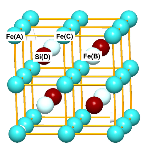
In the case of Fe3Si growth on GaAs the stoichiometry of the metallic films has an influence on their lattice parameterHerfort et al. (2003, 2004) and their long-range ordering.Jenichen et al. (2005) We find three types of diffraction maxima of Fe3Si. Fundamental reflections, i.e. (where is integer), are not sensitive to disorder. Their structure factor is . In the D structure of Fe3Si the Si atoms occupy the lattice position D, whereas the Fe atoms sit on the positions A,B,C, see Figure 1.Niculescu et al. (1976); Jenichen et al. (2005) The disorder is described by two types of order parameters and , which are the fractions of Si atoms occupying the Fe(B) and the Fe(A,C) sites, respectively. For (where is odd) the structure factor is
| (1) |
And for odd H,K,L we have
| (2) |
The lattice misfit between Fe3Si and GaAs is minimized for stoichiometric films. The lattice parameter of GaAs is 0.56325 nm whereas the lattice parameter of Fe3Si is 0.5654 nm.Hongzhi et al. (2007) From these values we obtain a mismatch below 0.4 %. In earlier work we found evidence for the presence of islands: The measured island height was larger than the nominal thickness of the deposited film.Kaganer et al. (2009) Later Fe3Si islands on GaAs were directly imaged by scanning tunneling microscopy, and it was found that the islands show a D03 structure, i.e. they were fully ordered.Noor et al. (2013) After coalescence of the Fe3Si islands a layer-by-layer growth of the metal was observed, which is typical for homoepitaxy of Fe3Si.Jenichen et al. (2007, 2008)
In general, the material Fe3Si with its high Curie temperature of about 567∘C is well suited for spintronic applications. The spin polarization of Fe3Si is about 45%.Ionescu et al. (2005) Room temperature spin injection from Fe3Si into GaAs was demonstrated.Herfort et al. (2005) The role of interdiffusion in the system Fe3Si/GaAs was investigated, and influence of interdiffusion on the ordering was found.Gusenbauer et al. (2011); Krumme et al. (2009) The ferromagnetism of the thin Fe3Si films arises at a nominal thickness of about 3 monolayers (MLs).Liou et al. (1993); Herfort et al. (2008); Noor et al. (2013) One ML corresponds to 0.28 nm.
The aim of the present work is a detailed structural characterization of the heteroepitaxial Fe3Si on GaAs(001). We directly image Fe3Si growth islands by cross-section high resolution transmission electron microscopy (HR TEM) and perform corresponding measurements of crystal truncation rods using grazing incidence X-ray diffraction of synchrotron radiation. The influence of the growth rate on long-range ordering is studied. A comparison of fundamental and superlattice maxima gives information about long-range ordering within the Fe3Si.Niculescu et al. (1976); Jenichen et al. (2005) Residual disordering near the Fe3Si/GaAs interface is revealed using the Z-contrast method in a probe-Cs-corrected scanning TEM with atomic resolution.
| sample | 1 | sample | 2 | sample | 3 | sample | 4 | |||||||||
|---|---|---|---|---|---|---|---|---|---|---|---|---|---|---|---|---|
| thickness | TS | vg | thickness | TS | vg | thickness | TS | vg | thickness | TS | vg | |||||
| (ML) | ∘C | (ML/h) | (ML) | ∘C | (ML/h) | (ML) | ∘C | (ML/h) | (ML) | ∘C | (ML/h) | |||||
| GaAs | 1071 | 580 | ./. | 1071 | 580 | ./. | 1071 | 580 | ./. | 1071 | 580 | ./. | ||||
| Fe3Si | 3 (4) | 200 | 71 | 0.48 | 3 (4) | 200 | 3 | 0.0 | 6 (7) | 200 | 71 | 0.45 | 7 (71) | 200 | 3 | 0.0 |
| Ge | 14 | 150 | ./. | ./. | ./. | 14 | 150 | ./. | ./. | ./. |
II Experimental
The GaAs(001) substrates were overgrown with a 350 nm thick GaAs buffer layer at a growth temperature TG = 580∘C. After cooling down this leads to a formation of an atomically flat and As-rich c(44) reconstructed GaAs(001) surface. Subsequently, the substrates were transferred under UHV conditions to a separate, As-free chamber with a base pressure of 110-10 mbar where the Fe3Si was grown at different growth rates (3 ML/h and 71 ML/h). Fe and Si where coevaporated and deposited on the GaAs substrate at TG = 200∘C.Herfort et al. (2003, 2004)
Two types of samples were compared (see Table 1), i.e. samples grown with a relatively high Fe3Si growth rate (samples 1 and 3) and samples grown with lower Fe3Si growth rate (samples 2 and 4). Growth rates and Fe3Si stoichiometry were determined via calibration measurements using X-ray diffraction peak position and thickness fringes.Herfort et al. (2004); Jenichen et al. (2007) In addition we measured Reflection high energy electron diffraction oscillations and X-ray oscillations of the layer-by-layer growth of Fe3Si. We have used these methods because the flux rates are relatively low and cannot be determined directly with the sufficient accuracy. Two different types of MBE systems were used, one with relatively low growth rateJenichen et al. (2003) due to geometrical reasons, the other with higher growth rate.Herfort et al. (2003) Two nominal Fe3Si film thicknesses were taken into account: 3 ML (before coalescence of growth islands, samples 1 and 2) and 6 ML (after coalescence of growth islands, samples 3 and 4). Some of the samples (samples 1 and 3) were capped with 4 nm of amorphous Ge deposited at TG = 150∘C, the remaining ones (samples 2 and 4) were characterized in–situ immediately after the growth. Sample 5 contains a 36 nm thick Fe3Si film on top of the GaAs(001) buffer layer. It was grown at high growth rate. The ordering of the thick Fe3Si film near the Fe3Si/GaAs interface is investigated using sample 5.
Synchrotron-based X-ray diffraction (XRD) was performed in grazing incidence geometry at the PHARAO U-125/2 KMC beamline of the storage ring BESSY II (Berlin). The photon energy was 10 keV, with an energy resolution of 10-4. The simulations of the crystal truncation rods were performed as in Ref. Kaganer et al., 2009 , where the disorder parameters and where taken into account.
The GaAs 222 and 002 reflections are quasiforbidden and in that way the corresponding Fe3Si maxima are not disturbed by an intense substrate reflection. In this manner the disorder parameter can be determined with high sensitivity. In the present work we restrict ourselves to this parameter, because the amount of material is extremely small and cannot be determined due to intense substrate contribution for odd H,K,L.
Cross-sectional TEM specimens were prepared by mechanical lapping and polishing, followed by Ar ion milling. A TEM JEOL JEM2100 F operated at 200 kV was used for high-resolution (HR) imaging. The probe-Cs-corrected JEOL ARM200 operated in the scanning TEM (STEM) mode at 200 kV was utilized for atomically resolved high-angle annular dark field imaging. In addition, corresponding image contrast simulations using the program JEMS allowed for a certain interpretation of the image contrast.Stadelmann (2016)
III Results
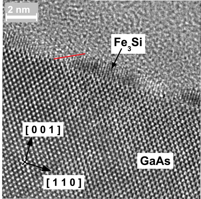
Fe3Si islands of sample 1 imaged by HR TEM (Figure 2) are approximately 4 MLs high and 3 nm in lateral size. The real height of 4 MLs is larger than the nominal film thickness 3 MLs, and so the coverage of the GaAs surface becomes smaller than 1.
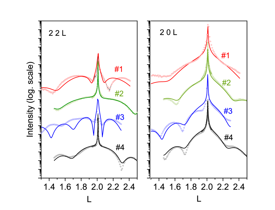
Figure 3 shows the L-scans of all the samples of the 20L and 22L crystal truncation rods measured by grazing incidence diffraction (GID) using synchrotron radiation. From comparison with simulations we obtain for sample 1 an island height of 4 MLs and a poor ordering of the Fe3Si islands (with = 0.48, see Table 1, cf. also Jenichen et al. (2005)). The 202 maximum is fundamental and not sensitive to disorder.Jenichen et al. (2005) Therefore we determined the island height from comparison of the experimental curve and the simulation of this 20L crystal truncation rod and used the same height for the simulation of the 22L-measurement as well. Obviously for the 22L-measurement the fringe period is deviating from the calculated value indicating inhomogeneity of the ordering.
The 202 diffraction maxima of Fe3Si and GaAs overlap without peak shift, i.e. the Fe3Si islands exhibit nearly ideal stoichiometry.Herfort et al. (2003, 2004) For sample 1 the 222 and 002 maxima have characteristic shapes with a strong reduction of the Fe3Si layer maxima, which are evidence for chemical disorder in the Fe3Si. The difference with respect to a fully ordered film becomes obvious from comparison with sample 2 (Figure 3). The 202 peaks of both samples are rather similar, because they are not sensitive to disorder, whereas the 222 peaks of the Fe3Si islands differ, because in sample 1 the Fe3Si is disordered, resulting in a reduced Fe3Si 222 peak intensity, and in sample 2 it is fully ordered with = 0.0 (see Table 1), and the Fe3Si 222 peak exhibits full intensity. Sample 3 contains a nominally 6 ML thick film, and was grown at high growth rate. It exhibits strong disorder with = 0.45. For sample 3 the thickness of the disordered region again does not coincide with the full film thickness due to inhomogeneous ordering resulting in different interference period lengths for fundamental and superlattice maxima, i.e. a disagreement of measurement and simulation. Sample 4 is a nominally (71) ML thick film, and was grown at low growth rate, and exhibits perfect ordering with = 0.0 (see Table 1). The measured thickness for this sample coincides with the nominal thickness, i.e. the coverage now equals one. The film is continuous now, all islands are coalesced. This would be the starting phase of Fe3Si homoepitaxy.
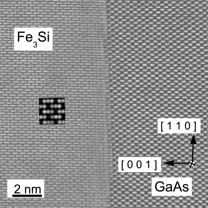
Figure 4 shows the Fe3Si/GaAs interface of sample 5 in a scanning transmission micrograph taken in the high-angle annular dark field (HAADF) mode of the STEM. The inset depicts a simulation for perfectly D03 ordered Fe3Si with characteristic Fe-triples. In the z-contrast mode the Fe atoms give the highest scattering intensity, whereas the Si atoms scatter with lower intensity.Pennycook and Jesson (1990) The GaAs crystal structure is nearly ideal, however the Fe3Si structure shows evidence of disordering near the interface, where the Fe-triples are blurred. The sample was grown at a growth rate of 71 ML/h. The disordering near the interface is connected to the disorder occuring during the starting phase of the epitaxial growth. We note, that a similar effect was obtained for the growth of lattice matched Co2FeSi Heusler alloy film on GaAs(001).Hashimoto et al. (2007) The role of interdiffusion should be stronger for lower growth rate, however, perfect ordering is found for the lower growth rate. In this way the disorder found in our case is rather a growth phenomenon.
Neglecting the anisotropy of Fe3Si we can make a rough estimate of the Fe3Si/GaAs(001) interface energy using the simple formula from Ref. de Gennes, 1985
| (3) |
where taking into account a contact angle (Figure 2), the surface energy of GaAs , and the surface energy of Fe3Si (see above). The limited accuracy of this estimate does not allow for any conclusions about the influence of the growth rate on the interface energy.
IV Conclusion
Thin Fe3Si islands and films grown on GaAs(001) exhibit long-range ordering which is depending on their growth rate. A sufficiently low enough growth rate can secure a fully ordered Fe3Si lattice, whereas a higher growth rate leads to a nearly fully disordered film, which is however still lattice matched. The disorder occurring in the starting phase of the growth seems to be the reason for disorder observed near the Fe3Si/GaAs interface.
V Acknowledgments
The authors thank V. Kaganer for helpful discussion and the simulation program for the X-ray data. We also thank H. Kirmse and T. Heil for the help with the HAADF micrograph shown in Figure 4. We are grateful C. Herrmann and H.-P. Schönherr for their support during the growth of the samples, and D. Steffen for preparation of the TEM-samples.
VI References
References
- Volmer and Weber (1926) M. Volmer and A. Weber, Z. phys. Chem. 119, 277 (1926).
- Raviswaran et al. (2001) A. Raviswaran, C.-P. Liu, J. Kim, D. G. Cahill, and G. Gibson, Phys. Rev. B 63, 125314 (2001).
- Kaganer et al. (2009) V. M. Kaganer, B. Jenichen, R. Shayduk, W. Braun, and H. Riechert, Phys. Rev. Lett. 102, 016103 (2009).
- Placidi et al. (2000) E. Placidi, M. Fanfoni, F. Archiprete, F. Patella, N. Motta, and A. Balzarotti, Mat. Sci. and Eng. B69-70, 243 (2000).
- Moll et al. (1996) N. Moll, A. Kley, E. Pehlke, and M. Scheffler, Phys. Rev. B 54, 8844 (1996).
- Hafner and Spisák (2007) J. Hafner and D. Spisák, Phys. Rev. B 75, 195411 (2007).
- Herfort et al. (2003) J. Herfort, H.-P. Schönherr, and K. H. Ploog, Appl. Phys. Lett. 83, 3912 (2003).
- Herfort et al. (2004) J. Herfort, H. P. Schoenherr, K. J. Friedland, and K. H. Ploog, J. Vac. Sci. Technol. B 22, 2073 (2004).
- Jenichen et al. (2005) B. Jenichen, V. M. Kaganer, J. Herfort, D. K. Satapathy, H. P. Schönherr, W. Braun, and K. H. Ploog, Phys. Rev. B 72, 075329 (2005).
- Niculescu et al. (1976) V. Niculescu, K. Raj, J. I. Budnick, T. J. Burch, W. A. Hines, and A. H. Menotti, Phys. Rev. B 14, 4160 (1976).
- Hongzhi et al. (2007) L. Hongzhi, Z. Zhiyong, M. Li, X. Shifeng, L. Heyan, Q. Jingping, L. Yangxian, and W. Guangheng, J. Phys. D: Appl. Phys. 40, 7121 (2007).
- Noor et al. (2013) S. Noor, I. Barsukov, M. S. Ozkan, L. Elbers, N. Melnichak, J. Lindner, M. Farle, and U. Koehler, J. Appl. Phys. 113, 103908 (2013).
- Jenichen et al. (2007) B. Jenichen, V. M. Kaganer, W. Braun, J. Herfort, R. Shayduk, and K. H. Ploog, Thin Solid Films 515, 5611 (2007).
- Jenichen et al. (2008) B. Jenichen, V. M. Kaganer, W. Braun, R. Shayduk, B. P. Tinkham, and J. Herfort, J. Mat. Sci.: Mater. Electron. 19, 199 (2008).
- Ionescu et al. (2005) A. Ionescu, C. A. F. Waz, T. Trypiniotis, C. M. Gürtler, H. Garcia-Miquel, J. A. C. Bland, M. E. Vickers, R. M. Dalgliesh, C. Langridge, Y. Bugoslavsky, Y. Miyoshi, L. F. cohen, and K. R. A. Ziebeck, Phys. Rev. B 71, 094401 (2005).
- Herfort et al. (2005) J. Herfort, H.-P. Schönherr, A. Kawaharazuka, M. Ramsteiner, and K. H. Ploog, J. Cryst. Growth 278, 666 (2005).
- Gusenbauer et al. (2011) C. Gusenbauer, T. Ashraf, J. Stangl, G. Hesser, T. Plach, A. Meingast, G. Kothleitner, and R. Koch, Phys. Rev. B 83, 035319 (2011).
- Krumme et al. (2009) B. Krumme, C. Weis, H. C. Herper, F. Stromberg, C. Antoniak, A. Warland, E. Schuster, P. Srivastava, M. Walterfang, K. Fauth, J. Minár, H. Ebert, P. Entel, W. Keune, and H. Wende, Phys. Rev. B 80, 144403 (2009).
- Liou et al. (1993) S. H. Liou, S. S. Malhotra, J. X. Shen, M. Hong, J. Kwo, H. S. Chen, and J. P. Mannaerts, J. Appl. Phys. 73, 6766 (1993).
- Herfort et al. (2008) J. Herfort, H.-P. Schönherr, and B. Jenichen, J. Appl. Phys. 103, 07B506 (2008).
- Jenichen et al. (2003) B. Jenichen, W. Braun, V. M. Kaganer, A. G. Shtukenberg, L. Däweritz, C. G. Schulz, and K. H. Ploog, Rev. Sci. Instr. 74, 1267 (2003).
- Stadelmann (2016) P. Stadelmann, Electron Microscopy Simulation progam JEMS, version 4.xx, http://www.jems-saas.ch/, Lausanne, (2016).
- Pennycook and Jesson (1990) S. J. Pennycook and D. E. Jesson, Phys. Rev. Lett. 64, 938 (1990).
- Hashimoto et al. (2007) M. Hashimoto, A. Trampert, J. Herfort, and K. H. Ploog, J. Vac. Sci. Technol. B 25, 1453 (2007).
- de Gennes (1985) P. G. de Gennes, Rev. of Mod. Phys. 57, 827 (1985).