Dimensionality reduction and band quantization induced by potassium intercalation in 1-HfTe2
Abstract
We have performed angle-resolved photoemission spectroscopy on transition-metal dichalcogenide 1-HfTe2 to elucidate the evolution of electronic states upon potassium (K) deposition. In pristine HfTe2, an in-plane hole pocket and electron pockets are observed at the Brillouin-zone center and corner, respectively, indicating the semimetallic nature of bulk HfTe2, with dispersion perpendicular to the plane. In contrast, the band structure of heavily K-dosed HfTe2 is obviously different from that of bulk, and resembles the band structure calculated for monolayer HfTe2. It was also observed that lightly K-dosed HfTe2 is characterized by quantized bands originating from bilayer and trilayer HfTe2, indicative of staging. The results suggest that the dimensionality-crossover from 3D (dimensional) to 2D electronic states due to systematic K intercalation takes place via staging in a single sample. The study provides a new strategy for controlling the dimensionality and functionality of novel quantum materials.
Controlling the dimensionality of materials is one of the key challenges in condensed matter physics because dimensionality plays a crucial role in determining exotic physical properties and quantum phenomena Novoselov1 ; Klitzing ; Cao ; Zeng ; Mak1 ; Mak2 ; Wang ; Xi1 ; Lu ; Xi2 ; Saito ; Mak3 . It is often seen that reduction of dimensionality from 3D to 2D causes emergence of novel physical properties absent in 3D bulk, as represented by massless Dirac fermions in graphene Novoselov1 , quantum Hall effect in semiconductor heterostructures Klitzing , valley-selective circular dichroism Cao ; Mak1 ; Zeng , and valley Hall effect Mak2 . Moreover, the 3D-to-2D crossover sometimes leads to more gigantic physical properties, as exemplified by a drastic increase in the superconducting transition temperature in monolayer FeSe Wang , the enhancement of charge-density-wave (CDW) transition temperature Xi1 and upper-critical field Lu ; Xi2 ; Saito in transition-metal dichalcogenides (TMDs). These drastic changes in physical properties upon reducing the dimensionality are known to be inherently linked to the modification of the electronic band structure such as the spin splitting caused by the inversion-symmetry breaking Zhu ; Nakata1 and the indirect-to-direct transition nature of band gap due to the absence of 3D chemical bonding Mak3 . Also, 2D systems are very sensitive to external stimuli like strain, charge doping, and electric field, so that the engineering of band structure is more feasible, making 2D systems a promising platform to explore novel physical properties.
Given the importance of controlling the dimensionality, a next important issue is how to control it. A widely used approach to reduce the dimensionality of materials from 3D to 2D is to mechanically or chemically exfoliate the sample Novoselov2 ; Joesen (top-down approach). This can lead to an exotic change in properties as highlighted by the realization of quantum Hall effect in graphene exfoliated from graphite Novoselov2 . A bottom-up approach such as deposition of atoms or molecules on a substrate using molecular-beam-epitaxy method Koma ; Zhang ; Nakata1 ; Nakata2 ; Sugawara or chemical-vapor-deposition technique Sutter ; Kim , is also useful. While these approaches have been successfully employed to explore unconventional physical properties associated with the reduction of dimensionality, a systematic control of dimensionality in these approaches needs great efforts because it requires one-by-one fabrication of various films with different thickness. As reported here, we have found a rather unexpected and effective way to systematically control the dimensionality and band structure of a TMD system.
In this Rapid Communication, we carried out a simple and useful approach to control the dimensionality and electronic structure on the surface of the TMD 1-HfTe2. Using angle-resolved photoemission spectroscopy (ARPES) for visualizing the band structure of 1-HfTe2, we first show that the pristine bulk compound is a typical semimetal with hole and electron pockets at the and M points in the Brillouin zone. Very surprisingly, our results also show that the original 3D electronic structure in bulk pristine 1-HfTe2 converts into a purely 2D electronic structure upon potassium (K) intercalation. Intriguingly, while the observed valence-band (VB) structure in pristine HfTe2 is well reproduced by the band calculations for bulk, those in lightly and heavily K-dosed HfTe2 well follow the calculated bands for and , respectively, providing evidence for dimensionality reduction and band quantization driven by K intercalation.
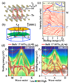
We have chosen HfTe2 as a test material to carefully monitor the evolution of electronic states upon K deposition, without complications from various orders (such as CDW and superconductivity) Brattas ; Hodul1 ; Hodul2 ; Klipstein ; Aminalragia-Giamini ; Mangelsen which are known to exist in many other TMDs. High-quality single crystals of 1-HfTe2 [see Fig. 1(a) for the crystal structure] were grown by the chemical-vapor-transport method Ueno . ARPES measurements were performed at the beamlines BL28 of Photon Factory, KEK and BL21B1 of Taiwan Light Source, NSRRC. First-principles band-structure calculations were carried out by a projector augmented wave method VASP with generalized gradient approximation (GGA) GGA . For details of experiments and calculations, see sections 1-3 of Supplemental Material.
First, we show the electronic states of pristine HfTe2. Figure 1(c) displays the energy distribution curves (EDCs) in the VB region measured along the M cut in the bulk Brillouin zone (BZ) [Fig. 1(b)] at photon energy () of 85 eV. We recognize several dispersive bands such as holelike bands centered at the point. One of these holelike bands crosses the Fermi level (), forming a small hole pocket at the point. A low-intensity but clear Fermi-edge cut-off is seen around the M point [see the inset in Fig. 1(c) and Fig. 2(c)], indicating a small electron pocket around the M point. These results confirm the semimetallic nature of HfTe2, consistent with previous transport measurements Klipstein ; Mangelsen and first-principles band-structure calculations Aminalragia-Giamini ; Mangelsen . To see the VB structure in more detail, we show in Figs. 1(d) and 1(e) the experimental band dispersions obtained by plotting the ARPES intensity as a function of wave vector () and binding energy () along high-symmetry cuts in the KM ( = 0) and AHL ( = ) planes, respectively. We also show the corresponding band dispersions calculated for bulk 1-HfTe2 for comparison. As shown in Fig. 1(d), the overall experimental VB dispersion such as the location of dispersive holelike bands at the point is well reproduced in the calculation when the calculated bands are shifted downward as a whole by 0.47 eV. These holelike bands are attributed to the Te 5 orbital. On the other hand, the electron pocket at the M point stemming from the Hf 5 orbital Aminalragia-Giamini ; Mangelsen is significantly larger in the calculation. This is not due to the imperfect compensation of electrons and holes in the experiment, but due to the overestimation of the semimetallic band overlap ( negative band gap) in the calculations ( 1 eV in contrast to 0.05 eV in experiments). Such overestimation was also recognized in previous band calculations of HfTe2 Aminalragia-Giamini ; Mangelsen and also in other TMDs such as TiSe2 Chen . While one may attribute such overestimation to the unoptimized interlayer coupling, we found that the change in the -axis lattice constant ( layer spacing) in the calculation is insufficient to correctly reproduce the experimental band structure, suggesting that there are other factors to overestimate the band gap in the calculation (see section 4 of Supplemental Material for details). As shown in Figs. 1(d) and 1(e), while the overall experimental VB dispersion looks similar between the = 0 and plane, a closer look reveals some characteristic differences such as the number of holelike bands and presence/absence of a flat dispersion at 2.6 eV for = 0 / = , indicating the 3D nature of the band structure. It is noted that the agreement of band structure between experiments and calculations is relatively poor in the = plane compared to that in the = 0 plane. In fact, it was necessary to shift the calculated VB dispersions upward by 0.28 eV to make a better match to the experimental data for = .
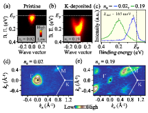
Now that the band structure of pristine HfTe2 is established, next we demonstrate how the electronic states are influenced by K deposition. One would naturally expect that K atoms donate electrons into the HfTe2 top layers. This is clearly visible as a downward shift of the electronlike band at the M point, as shown in Figs. 2(a) and 2(b). We have estimated the energy shift () to be 165 meV by comparing the peak position of EDCs as shown in Fig. 2(c). The electron doping with K deposition is also seen in the change of Fermi surface [Figs. 2(d) and 2(e)]. Upon K deposition, the hole pocket at the point disappears and at the same time the ellipsoidal electron pocket at the M point expands. Hereafter we label each sample with the size of electron pocket at the M point (See Section 5 of Supplemental Material for the detailed procedure), which corresponds to the electron density in a unit layer. For example, samples in Figs. 2(d) and 2(e) are labeled =0.02 and =0.19 samples, respectively.
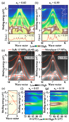
Figures 3(a) and 3(b) show a side-by-side comparison of experimental band dispersions between pristine (=0.02) and heavily K-deposited (=0.19) sample. Although the electron pocket at the M point is shifted downward by K deposition as expected, the data show several anomalous changes in the band structure which cannot be explained within a simple rigid-band scheme. For example, in the =0.02 sample, we observe three holelike bands centered at the point; two topped at around and one topped at 1 eV. On the other hand, only two holelike bands (topped at 0.1 and 0.75 eV) exist in the =0.19 sample. Such a difference in the number of bands is also highlighted by the representative momentum distribution curve (MDC) in the bottom panels of Figs. 3(a) and 3(b) which signify the presence of broad three peaks and sharp two peaks in the M cut (also in the K cut) for = 0.02 and 0.19, respectively. As shown in Figs. 3(a) and 3(b), while a relatively flat band at 2.6 eV appears to shift downward upon K deposition, a new M-shaped band emerges slightly above this band ( 2.5 eV) in the =0.19 sample. To clarify the origin of such anomalous variation of the band structure, we compare in Figs. 3(c) and 3(d) the experimental band structure for = 0.19 with the calculated band structure for bulk and monolayer HfTe2, respectively. One can see that the calculated band structure for monolayer shows a good agreement with the experimental band structure (except for the electron pocket at the M point), while the calculated band structure for the bulk apparently shows some disagreements such as in the location of the holelike bands and the absence of the M-shaped band. This suggests that the originally bulk-like band dispersion is “converted” into the monolayer-like one upon K deposition. Such a change to the monolayer-like behavior is also confirmed by performing photon-energy-dependent ARPES measurements that signify a finite energy dispersion along in the pristine (=0.02) sample [Fig. 3(f)] in line with the band calculation [Fig. 3(e)], in contrast to no discernible dispersion in the =0.19 sample [Fig. 3(g)]. These results indicate that the K deposition switches the dimensionality of electronic structure from 3D to 2D. We found that such a 3D-2D transition is accompanied by a sharpening of the spectral line shape highlighted by the comparison of EDC at the point between = 0.02 and 0.19 in Fig. 3(b), which likely reflects absence of -broadening effect and reduced contribution of photoelectron lifetime for = 0.19.
To gain further insight into the origin of observed dimensionality change, we investigated the evolution of electronic states for various K-deposition time and show the ARPES intensities for a series of in Figs. 4(a)-4(d). This plot again confirms that the number of bands are apparently different between = 0.02 and 0.19, reflecting the dimensionality change. One can also see that the band structures for = 0.19 and 0.25 are very similar to each other. This suggests that the 2D nature of electronic states is more or less established at = 0.19 and further K deposition simply leads to extra electron doping with a small constant shift of the overall band structure to higher binding energies. We comment here that, while a previous study for epitaxy-grown atomic-layer HfTe2 thin film on AlN Aminalragia-Giamini reported the Dirac-semimetal phase characterized by the Dirac-cone band at the point, the present result shows no upper Dirac-cone-like band for monolayer HfTe2 [Fig. 4(d)] (see Section 5 of Supplemental Material for details). This difference may be attributed to a substrate induced effect in epitaxial atomic-layer HfTe2 film on AlN compared to the present study.
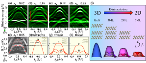
Finally, we present another very important finding. We found that the experimental band structure for = 0.05 shows unexpected behavior at energies away from . As highlighted by the area enclosed by red rectangle in Fig. 4(b), there exist three holelike bands topped at the range of 1-1.7 eV. Such multiple bands are absent in other samples, and hence they are likely a characteristic of an intermediate state between 3D ( = 0.02) and 2D ( = 0.19 - 0.25). To obtain further insight into the origin of such subband feature, we compare the ARPES-derived band dispersion [Fig. 4(e)] with the calculations for multilayer HfTe2 [Figs. 4(f), 4(g), and 4(h)]. One can see that band A is due to the bulk band since its shape and energy position are well reproduced by the calculation for bulk HfTe2 as shown in Fig. 4(f). This assignment is also corroborated with the observation of a similar band in the pristine sample ( = 0.02) [Fig. 4(a)]. On the other hand, bands B and C show a reasonable agreement with the calculated topmost quantized bands for trilayer and bilayer HfTe2, respectively. This implies that the surface of the = 0.05 sample is inhomogeneous in terms of the K concentration, and different domains coexist at the surface. It is thus likely that we simultaneously detect three domains (, bulk, trilayer, and bilayer) in the ARPES data [Fig. 4(b)] for = 0.05. It is noted that a weak feature labeled D in Fig. 4(e) may be ascribed to a mixture of the second and/or third quantized orbital in trilayer and bilayer domains.
We discuss the origin of observed intriguing change in the band structure. We found no obvious change in the LEED (low-energy-electron-diffraction) pattern upon K deposition, in particular, regarding the location of the LEED spot. This suggests that the in-plane lattice parameter does not change and no surface reconstruction takes place (see section 7 of Supplemental Material for details). Thus, the observed evolution of band structure upon K deposition in Figs. 2-4 is not ascribed to the structural modulation of the HfTe2 layer itself. A plausible explanation for the observation of monolayer-like band dispersion for = 0.19 and 0.25 is that K atoms are intercalated into the van der Waals gap of HfTe2 layers around the surface, as naively understood by referring to stage-one graphite intercalation compounds (GICs) where atoms are intercalated in all the available van der Waals gaps. Since K atoms are randomly placed in HfTe2 as inferred from the absence of band folding and additional LEED spots after K deposition, the K atoms do not enhance the interlayer coupling unlike the case of GICs where the periodic arrangement of intercalant atoms would promote the 3D nature of materials. In contrast, in the case of HfTe2, each layer is effectively isolated from adjacent layers due to the increased layer spacing, leading to enhancement of monolayer-like nature. A similar behavior has been observed in K-intercalated MoS2 Eknapakul1 and H-intercalated graphene on SiC H-SiC . On the other hand, besides the monolayer-like feature, we found that a multiple staging from stage-two to stage-three takes place at the surface of a single sample and gives rise to emergence of several quantized bands in the lightly K-deposited regime ( = 0.05). This finding is of particular significance since we could experimentally demonstrate that the dimensionality of the electronic states (in other words, staging of the intercalation) around the surface can be and controlled by the simple K-deposition technique.
The above quantization picture is further corroborated by considering the orbital character for the observed subbands. As visible in Fig. 4(b), the band quantization is well resolved only for the bands located at 1-2 eV. These bands originate from the orbital which is highly dispersive along the direction, as seen in Fig. 3(e). This situation is favorable for forming the quantized bands since the quantum confinement occurs along the direction (perpendicular to the surface). In contrast, the and orbitals are unlikely to be well quantized because of their weak dispersion; this is indeed inferred from the absence of subbands for the -derived flat band at 2.6 eV in Figs. 4(a)-4(d) [see also Fig. 3(e)]. It is worthwhile to note here that the previous study reported similar subbands after Na intercalation in HfSe2 Eknapakul2 . However, the mechanism of subband formation is totally different from the present case since the subbands of Na-intercalated HfSe2 have a character and they originate from the in-plane lattice strain Eknapakul2 . This is also consistent with the ARPES and LEED data (see section 7 of Supplemental Material) of HfTe2 which show no discernible variation of the in-plane lattice constant upon K intercalation in support of a weak strain effect. The present study demonstrates for the first time that the band quantization and dimensionality of electronic states can be manipulated by a simple deposition of atoms on the sample surface, as highlighted in Fig. 4(i).
We emphasize that the method proposed here to control the dimensionality and visualize the electronic states is useful since it can be performed on a single sample; this could be contrasted to the so-far established exfoliation and MBE techniques in which systematic control is rather difficult because they require one-by-one fabrication of various films with different thickness. Also, it is expected that our method can be widely applicable to other layered materials including TMDs if the condition of intercalation such as the species of alkali metals and evaporation temperature is optimized for each material (this point is important since the intercalation/adsorption condition would strongly depend on the combination of alkali-metal elements and constituent elements of TMDs Biswas ; Kang ). While we selected HfTe2 to monitor the evolution of electronic states to avoid complications from various orders Brattas ; Hodul1 ; Hodul2 ; Klipstein ; Aminalragia-Giamini ; Mangelsen and to effectively demonstrate controllability of dimensionality, a choice of other TMDs would provide us a precious opportunity to study in a systematic way the interplay between dimensionality and various exotic physical properties, such as unconventional superconductivity Lu ; Xi2 ; Saito , ferromagnetism Bonilla , topological phase transition, and quantum spin Hall effect Qian ; Tang ; Fei ; Wu . Experiments combining surface spectroscopies and magneto-transport measurements in K-deposited TMDs would be highly desired in future.
In conclusion, our ARPES study on HfTe2 revealed a rich variation of electronic structure upon K intercalation associated with the 3D-to-2D crossover. We proposed a new technique to control the dimensionality of electronic states at the surface by simple K deposition. The present result would serve as a foundation for investigating the interplay between dimensionality and exotic physical properties in TMDs and other layered quantum materials.
Acknowledgements.
We thank T. Kato, K. Hori, K. Owada, T. Nakamura, H. Oinuma, K. Shigekawa, and D. Takane for their assistance in the ARPES measurements. We also thank KEK-PF for access to beamline BL28 (Proposal number: 2018S2-001) and NSRRC-TLS for beamline BL21A2. This work was supported by JST-CREST (No: JPMJCR18T1), MEXT of Japan (Innovative Area “Topological Materials Science” JP15H05853), JSPS (JSPS KAKENHI No: JP17H01139, JP26287071, JP18H01160, JP18H01821, 18K18986, JP25107003, JP25107004, and 18J10038), Grant for Basic Science Research Projects from the Sumitomo Foundation, and Murata Science Foundation. Y. N. acknowledges support from GP-Spin at Tohoku University.References
- (1) K. S. Novoselov, A. K. Geim, S. V. Morozov, D. Jiang, M. I. Katsnelson, I. V. Grigorieva, S. V. Dubonos, and A. A. Firsov, Nature 438, 197 (2005).
- (2) K. V. Klitzing, G. Dorda, and M. Pepper, Phys. Rev. Lett. 45, 494 (1980).
- (3) T. Cao, G. Wang, W. Han, H. Ye, C. Zhu, J. Shi, Q. Niu, P. Tan, E. Wang, B. Liu, and J. Feng, Nat. Commun. 3, 887 (2012).
- (4) H. Zeng, J. Dai, W. Yao, D. Xiao, and X. Cui, Nat. Nanotech. 7, 490 (2012).
- (5) K. F. Mak, K. He, J. Shan, and T. F. Heinz, Nat. Nanotech. 7, 494 (2012).
- (6) K. F. Mak, K. L. McGill, J. Park, and P. L. McEuen, Science 344, 1489 (2014).
- (7) Q. Y. Wang, Z. Li, W. H. Zhang, Z. C. Zhang, J. S. Zhang, W. Li, H. Ding, Y. B. Ou, P. Deng, K. Chang, J. Wen, C. L. Song, K. He, J. F. Jia, S. H. Ji, Y. Y. Wang, L. L. Wang, X. Chen, X. C. Ma, and Q. K. Xue, Chin. Phys. Lett. 29, 037402 (2012).
- (8) X. Xi, L. Zhao, Z. Wang, H. Berger, L. Forr, J. Shan, and K. F. Mak, Nat. Nanotechnol. 10, 765 (2015).
- (9) J. M. Lu, O. Zheliuk, I. Leermakers, N. F. Q. Yuan, U. Zeitler, K. T. Law, and J. T. Ye, Science 350, 1353 (2015).
- (10) Y. Saito, Y. Nakamura, M. S. Bahramy, Y. Kohama, J. Ye, Y. Kasahara, Y. Nakagawa, M. Onga, M. Tokunaga, T. Nojima, Y. Yanase, and Y. Iwasa, Nat. Phys. 12, 144 (2015).
- (11) X. Xi, Z. Wang, W. Zhao, J. -H. Park, K. T. Law, H. Berger, L. Forr, J. Shan, and K. F. Mak, Nat. Phys. 12, 139 (2016).
- (12) K. F. Mak, C. Lee, J. Hone, J. Shan, and T. F. Heinz, Phys. Rev. Lett. 105, 136805 (2010).
- (13) Z. Y. Zhu, Y. C. Cheng, and U. Schwingenschlgl, Phys. Rev. B 84, 153402 (2011).
- (14) Y. Nakata, K. Sugawara, S. Ichinokura, Y. Okada, T. Hitosugi, T. Koretsune, K. Ueno, S. Hasegawa, T. Takahashi, and T. Sato, npj 2D Mater. Appl. 2, 12 (2018).
- (15) K. S. Novoselov, D. Jiang, F. Schedin, T. J. Booth, V. V Khotkevich, S. V Morozov, and A. K. Geim, Proc. Natl. Acad. Sci. 102, 10451 (2005).
- (16) P. Joesen, R. F. Frindt, and S. R. Morrison, Mater. Res. Bull. 21, 457 (1986).
- (17) A. Koma, K. Sunouchi, and T. Miyajima, Microelectron. Eng. 2, 129 (1984).
- (18) Y. Zhang, T. R. Chang, B. Zhou, Y. T. Cui, H. Yan, Z. Liu, F. Schmitt, J. Lee, R. Moore, Y. Chen, H. Lin, H. T. Jeng, S. K. Mo, Z. Hussain, A. Bansil, and Z. X. Shen, Nat. Nanotech. 9, 111 (2014).
- (19) Y. Nakata, K. Sugawara, R. Shimizu, Y. Okada, P. Han, T. Hitosugi, K. Ueno, T. Sato, and T. Takahashi, NPG Asia Mater. 8, e321 (2016).
- (20) K. Sugawara, Y. Nakata, R. Shimizu, P. Han, T. Hitosugi, T. Sato, and T. Takahashi, ACS Nano 10, 1341 (2016).
- (21) P. W. Sutter, J. I. Flege, and E. A. Sutter, Nat. Mater. 7, 406 (2008).
- (22) D. Kim, D. Sun, W. Lu, Z. Cheng, Y. Zhu, D. Le, T. S. Rahman, and L. Bartels, Langmuir 27, 11650 (2011).
- (23) L. Brattas and A. Kjekshus, Acta Chem. Scand. 27, 1290 (1973).
- (24) D. Hodul and M. J. Sienko, Physica 99B, 215 (1980).
- (25) D. T. Hodul and A. M. Stacy, J. Phys. Chem. Solids 46, 1447 (1985).
- (26) P. C. Klipstein, D. R. P. Guy, E. A. Marseglia, J. I. Meakin, R. H. Friend, and A. D. Yoffe, J. Phys. C: Solid State Phys. 19, 4953 (1986).
- (27) S. Aminalragia-Giamini, J. Marquez-Velasco, P. Tsipas, D. Tsoutsou, G. Renaud, and A. Dimoulas, 2D Mater. 4, 015001 (2017).
- (28) S. Mangelsen, P. G. Naumov, O. I. Barkalov, S. A. Medvedev, W. Schnelle, M. Bobnar, S. Mankovsky, S. Polesya, C. Näther, H. Ebert, and W. Bensch, Phys. Rev. B 96, 205148 (2017).
- (29) K. Ueno, J. Phys. Soc. Jpn. 84, 121015 (2015).
- (30) G. Kresse and J. Furthmuller, Phys. Rev. B 54, 11169 (1996).
- (31) J. P. Perdew, K. Burke and M. Ernzerhof, Phys. Rev. Lett. 77, 3865 (1996).
- (32) P. Chen, Y.-H. Chan, X.-Y. Fang, Y. Zhang, M.Y. Chou, S.-K. Mo, Z. Hussain, A.-V. Fedorov, and T.-C. Chiang, Nat. Commun. 6, 8943 (2015).
- (33) T. Eknapakul, P. D. C. King, M. Asakawa, P. Buaphet, R. H. He, S. K. Mo, H. Takagi, K. M. Shen, F. Baumberger, T. Sasagawa, S. Jungthawan, and W. Meevasana, Nano Lett. 14, 1312 (2014).
- (34) C. Riedl, C. Coletti, T. Iwasaki, A. A. Zakharov, and U. Starke, Phys. Rev. Lett. 103, 246804 (2009).
- (35) T. Eknapakul, I. Fongkaew, S. Siriroj, W. Jindata, S. Chaiyachad, S. K. Mo, S. Thakur, L. Petaccia, H. Takagi, S. Limpijumnong, and W. Meevasana, Phys. Rev. B 97, 201104(R) (2018).
- (36) D. Biswas, Alex M. Ganose, R. Yano, J. M. Riley, L. Bawden, O. J. Clark, J. Feng, L. Collins-Mcintyre, M. T. Sajjad, W. Meevasana, T. K. Kim, M. Hoesch, J. E. Rault, T. Sasagawa, David O. Scanlon, and P. D. C. King, Phys. Rev. B 96, 085205 (2017).
- (37) M. Kang, B. Kim, S. H. Ryu, S. W. Jung, J. Kim, L. Moreschini, C. Jozwiak, E. Rotenberg, A. Bostwick, and K. S. Kim, Nano Lett. 17, 1610 (2017).
- (38) M. Bonilla, S. Kolekar, Y. Ma, H. C. Diaz, V. Kalappattil, R. Das, T. Eggers, H. R. Gutierrez, M. H. Phan, and M. Batzill, Nat. Nanotech. 13, 289 (2018).
- (39) X. Qian, J. Liu, L. Fu, and J. Li, Science 346, 1344 (2014).
- (40) S. Tang, C. Zhang, Di. Wong, Z. Pedramrazi, H. Z. Tsai, C. Jia, B. Moritz, M. Claassen, H. Ryu, S. Kahn, J. Jiang, H. Yan, M. Hashimoto, D. Lu, R. G. Moore, C. C. Hwang, C. Hwang, Z. Hussain, Y. Chen, M. M. Ugeda, Z. Liu, X. Xie, T. P. Devereaux, M. F. Crommie, S. K. Mo, and Z. X. Shen, Nat. Phys. 13, 683 (2017).
- (41) Z. Fei, T. Palomaki, S. Wu, W. Zhao, X. Cai, B. Sun, P. Nguyen, J. Finney, X. Xu, and D. H. Cobden, Nat. Phys. 13, 677 (2017).
- (42) S. Wu, V. Fatemi, Q. D. Gibson, K. Watanabe, T. Taniguchi, R. J. Cava, and P. Jarillo-Herrero, Science 359, 76 (2018).