ABSense: Sensing Electromagnetic Waves on Metasurfaces via Ambient Compilation of Full Absorption
Abstract
Metasurfaces constitute effective media for manipulating and transforming impinging EM waves. Related studies have explored a series of impactful MS capabilities and applications in sectors such as wireless communications, medical imaging and energy harvesting. A key-gap in the existing body of work is that the attributes of the EM waves to-be-controlled (e.g., direction, polarity, phase) are known in advance. The present work proposes a practical solution to the EM wave sensing problem using the intelligent and networked MS counterparts-the HyperSurfaces (HSFs), without requiring dedicated field sensors. An nano-network embedded within the HSF iterates over the possible MS configurations, finding the one that fully absorbs the impinging EM wave, hence maximizing the energy distribution within the HSF. Using a distributed consensus approach, the nano-network then matches the found configuration to the most probable EM wave traits, via a static lookup table that can be created during the HSF manufacturing. Realistic simulations demonstrate the potential of the proposed scheme. Moreover, we show that the proposed workflow is the first-of-its-kind embedded EM compiler, i.e., an autonomic HSF that can translate high-level EM behavior objectives to the corresponding, low-level EM actuation commands.
Index Terms:
Metasurfaces, HyperSurfaces, EM sensing, nano-networks.I Introduction
Metasurfaces (MS) are highly efficient media for the manipulation of electromagnetic (EM) waves in custom and even unnatural ways. Wave attributes such as the direction of reflection, polarization [1], and the amount of absorption [2], among others, can be controlled with unprecedented accuracy. The outstanding principles MS have been already proven in the microwave, Terahertz (THz), and optical regimes [3], finding their way into a plethora of applications [4, 5, 6].
The basis for the MS operation is the Huygens principle, which states that any EM wavefront can be traced back to a planar distribution of currents [6]. In that sense, a MS acts as a canvas of currents comprising: i) passive elements acting as sub-wavelength antennas receiving impinging waves, i.e., inductive current sources, and ii) active elements such as PIN diodes acting as current flow manipulators. The active elements can be externally-biased, transforming the currents to follow a planar distribution that corresponds to a required wavefront. Thus, any overall manipulation of the impinging EM waves can be attained, e.g., anomalous steering, polarization and phase alteration, partial attenuation or even full absorption. HSFs are the intelligent, networked variation of MSes, which include an embedded nano-network and a gateway [7]. The nano-network collectively controls the biasing of the active elements in a distributed, autonomic manner, while the gateway connects the nano-network to the HSF-external world via a standard protocol (e.g., WiFi, Bluetooth, etc.).
It is a widespread practice to design MSes (and HSFs) assuming that the impinging wave attributes are known [6]. Nevertheless, this is rarely the case in a broad set of applications where the availability of EM sensing systems becomes a necessity. Currently, the wave attributes can be sensed via HSF-external systems and devices (e.g., d-dot sensors) [8]. However, this approach is not space-granular, since the EM field quantities are sensed i) on average and ii) at one point near or on the HSF gateway. Incorporating multiple such sensors in the HSF adds up to its assembly complexity and overall cost. Moreover, d-EM field sensors are currently size-able, posing novel minification challenges.
The present study proposes a wave sensing approach that operates without specialized sensory hardware and exploiting the HSF networking capabilities instead. The key idea is to sense the attributes of an impinging wave by fully absorbing it. Full absorption of impinging EM waves is well-studied MS capability [6]. When the surface impedance of the HSF is matched perfectly to the impinging wave, its power dissipates on the passive and active elements, at the same time serving the dual purpose of identifying the condition for perfect absorption. Thus, we use the embedded controller network within the HSF to intelligently iterate over the active element states and obtain the one yielding maximal dissipated power across the active elements. Then, we employ a static lookup table (provided by the HSF manufacturer) that contains the actuator states to achieve full absorption for specific impinging wave cases. The best matching entry is picked as the estimate of the impinging wave attributes. Apart from acting as a wave sensing scheme, the proposed approach is also a form of an ambient EM Compiler [9], since the nano-nodes collectively tune the HSF to attain a macroscopic functionality, i.e., the full absorption of an unknown EM wave.
II Related Studies
Metasurfaces are highly effective systems for controlling different aspects of EM waves (wavefront [10], collimation [11], polarization [12], dispersion [13], controllable absorption [14]), especially if they are tunable thus offering the ability to perform multiple functionalities and switch between them at will [3]. In recent years, interest has mainly focused on incorporating voltage-controlled actuation elements inside each unit cell, thus providing a means of dynamically tuning the surface impedance of the metasurface to external EM waves. This is because voltage-controlled elements can be readily controlled by an external controller, such as an Field Programmable Gate Array (FPGA), thus allowing for centrally controlling the metasurface response. The commonly integrated elements are PIN switch [15] or varactor [16] diodes, allowing for a broad range of functionalities ranging from wavefront manipulation, beam splitting, and polarization control. However, switch diodes allow for obtaining two discrete states of the surface impedance; it can be extended to when unit cells are clustered together to allow for -bit encoding, but is typically limited to or [15] since the resulting supercell must be subwavelength to remain in the metasurface regime. On the other hand, varactor diodes allow for continuous control but only over the reactive part of the surface impedance, thus providing the ability to tune the phase of the impinging wave but not its amplitude.
Recently, it has been shown that having the ability to continuously control both the reactive and resistive part of the complex surface impedance leads to maximum freedom over the available functionalities [17]. This can be achieved by integrating elaborate controller chips in each unit cell that can provide a complex input impedance (). Further enhancing this concept by forming a nano-network of the controllers defines the HyperSurface (HSF) paradigm [18, 7]. In a nutshell, the HyperSurface entails the passive meta-atom enhanced with an actuation module, a computation and communication module for exchanging data with other cells, and a gateway for communicating with HSF-external entities, such as receiving cell actuation commands and diffusing them for propagation within the inter-cell network. A prominent example of the applications enabled by HSFs are employing mitigation strategies for fault tolerance [19] or deploying programmable wireless environments [18, 20, 21, 5].
Here, we demonstrate a different possibility enabled by the rich HSF capabilities. Specifically, we demonstrate sensing of the characteristics, i.e., direction of incidence (measured by the spherical coordinate angles and ) and polarization (TE or TM), of the impinging wave. Similar functionalities have been demonstrated in plasmonic metasurfaces incorporating pixelated photodetectors strictly for polarization detection [22] and for orbital angular momentum detection enabled through the decomposition of the transmitted waves impinging on a properly designed metasurface [23]. In our approach we utilize the controllers integrated in the HSF configuration. In particular, we rely on the fact that by fully absorbing the incident wave the power dissipated on the controllers is maximized. More specifically, we monitor the dissipated power on the actuation elements themselves, thus avoiding extra sensing circuitry which would increase the complexity. Moreover, the proposed sensory system is autonomic, not requiring HSF-external computing or communication elements [8]. Additionally, to be best of the authors’ knowledge, the present work also constitutes the first application of distributed consensus algorithms [24, 25] as the enabler for the autonomic and collective operation of nano-networks. In this aspect, we note that related works have studied controlled flooding [26, 27], peer-to-peer [28, 26, 29, 30, 31] and nature-inspired alternatives [32].
It is noted that impressive further capabilities of metasurfaces has been recently demonstrated, promising novel expansions of the HyperSurface concept. Estakhri et al have showcased metastructure design processes able to serve as analog solvers to integral problems [33]. La Spada et al have proposed design workflows for curvilinear metasurfaces exerting arbitrary control over surface EM currents [34], as well as near-zero index wires [35]. Finally, graphene has also been extensively studied for frequency-tunable THz metasurfaces, since its conductivity can be dynamically modulated via electrical, magnetic and optical means [36].
III The proposed scheme
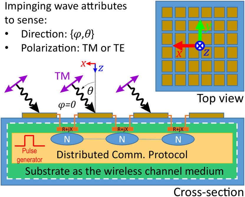
We consider a generic HSF architecture as shown in Fig. 1. From its physical aspect, it comprises the common passive and active elements of a metasurface. Additionally, it includes a wireless nano-network embedded within the HSF material, with each nano-node being responsible for the control of one active element. Notably, the HSF material also constitutes the wireless channel medium for the communicating nano-nodes [37, 38]. A distributed communications protocol is employed by the nodes at the application layer, as described later in this Section. The nano-network is supplied with power via an energy pulse generator, which also serves as a rudimentary clock as discussed later. The power pulses can be of any spectrum, such as microwaves, visible light, etc. [39]. A planar wave impinges upon the HSF, with a specific direction and polarization, as illustrated in Fig. 1. The objective is to employ the nano-network capabilities in order to detect these characteristics of the wave, i.e., direction and polarization. The proposed process executed by the HSF as a whole is denoted as ABSense and formulated in pseudo-code as Algorithm. 1.
The goal of the ABSense scheme is to sense the impinging wave attributes by: i) detecting the active element configurations that leads to the full absorption of the wave, and ii) deducing the best matching wave attributes by reversing a hashmap provided by the HSF manufacturer. This hashmap, denoted as , corresponds any parameterized EM function supported by the HSF to the active element state per node to achieve it. For instance, an entry of can be written as:
| (1) |
Treating and the impinging wave as inputs, the ABSense workflow is as follows. Signaled and synchronized by the pulse generator, each nano-node iterates over its possible active element states. All nodes move along their iterations in lock-step (detailed below), resulting each time into a uniform surface impedance across the HSF, which will eventually match the impinging wave. For each state , a node obtains a corresponding measurement of power flowing via its active element, . Susceptibility to noise and errors is taken into account. The state that yields the maximum is communicated to the nano-network as a whole via a distributed consensus approach, and an average value, , is obtained. Finally, using the map in reverse, each nano-node obtains the best matching parameterized function and, hence, the best matching wave attributes as well.
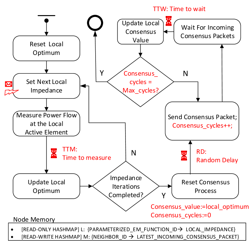
We proceed to detail the operation of each nano-node in Fig. 2. It comprises two phases, the iteration over local active element states (a set of impedance values ) to detect the one () yielding the maximum power flow, and the consensus phase to obtain the . From another point of view, this phase is also an ambient compilation of an EM functionality, since the nano-nodes self-tune the HSF to perform a full EM wave absorption [9]. The iteration phase is initialized by resetting the variable. Subsequently, the nodes are iterating over all their impedance values, orchestrated by the pulse/power generator (considered to be physically decoupled from the inter-nanonode packet exchange process). We assume that the pulse generator emits its energy in the form of pulse sequences representing integer identifiers of the nodes’ impedance values. This pulse emission and orchestration via impedance value identifier broadcast process is continuous. The identifiers are broadcast given enough time for the impedance value to be setup and the power measurement to be obtained (TTM: time to measure), accounting for clock drifts and signal processing variations.
The consensus phase then operates as follows. Each node initializes
its consensus value as ,
and broadcasts it to all nano-nodes in its vicinity. A random delay
(RD) is considered to minimize packet collisions. The broadcast
date has the form of a packet structured as follows:
SENDER_ID (8 bit)
R (32 bits)
X (32 bits)
where the sender ID is an integer identifier of the sending node.
During a fixed time interval (TTW: time to wait), each receiving
node collects incoming packets while also keeping a log of the average
reception power for each one. This information is kept in a hash-map,
,
with sender IDs as keys, as shown in Fig. 2. Subsequently,
each node obtains a first estimate of
as:
| (2) |
where is the personal weight that the node gives to its local value, and is the weight assigned to the incoming consensus packets. We consider that the values are proportional to the reception power of the corresponding incoming packets, and are normalized to comply to the condition:
| (3) |
The consensus process converges iteratively, allowing each node to obtain the actual value [25]. The consensus process is allowed to run for a maximum number of send/receive packet cycles (max_cycles), upon which it yields the estimated . The process then concludes by reversing to detect the full EM absorption parameterized function that best matches the estimated and, subsequently, it returns the corresponding EM function parameters as the most probable EM wave attributes.
The process as a whole can be immediately restarted, should the HSF tile be operating in a dedicated sensory role, i.e., to sense EM waves and inform other HSF units to adapt accordingly. Alternatively, having obtained the sensory information, the same HSF tile can autonomically apply a different EM manipulation function, such as steering the sensed wave towards a direction. The mode of operation can be adapted to the application scenario at hand.
IV Evaluation
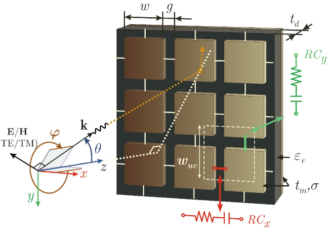
We evaluate the proposed scheme using simulations. The evaluation combines full wave simulations conducted in CST [40] and nano-network simulations conducted in the AnyLogic platform [41]. The full wave simulations produce a dataset of power flow values at each active element in a specific HSF design (shown in Fig. 3) for a variety of impinging wave directions and polarizations, and for any active element state each time. This dataset is then passed on to the nano-network simulator which follows the process described in Section III.
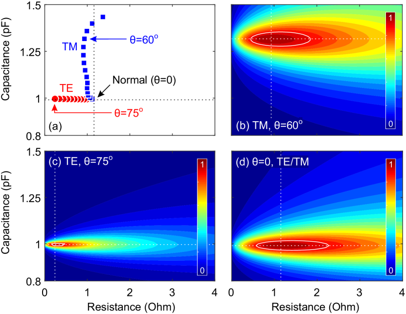
The HSF used in this work consists of an array of square metallic patches over a thin metal-backed dielectric (Fig. 3 illustrates a sub-part for ease of presentation). The unit-cell includes two lumped elements modeled as complex-valued (resistive and capacitive) loads that connect neighbouring metallic patches, along the - and -directions. The corresponding unit-cell, framed with a white border, is designed for 5 GHz operation and its main parameters are: mm, mm, mm, mm, mm, and S/m. For normal incidence, perfect absorption of - and -polarized plane waves is achieved when Ohm and pF.
Sample visual hash-maps that are used to link the values required for perfect absorption with incidence direction and polarization are depicted in Fig. 4: panel (a) shows the required for TE/TM polarized incidence as the elevation angle varies, for azimuth angle , i.e., when is the plane of incidence; panels (b)-(d) show the absorption coefficient for waves of three different incidence directions and polarizations as the values are varied; the white circles mark the regions where the attenuation coefficient is higher than 0.9 (corresponding to reflection coefficient of dB or lower), and the white crosses mark the values leading to perfect absorption. Note that only the lumped elements oriented parallel to the impinging -field affect the resonance of the unit-cell; for instance, when the TE (perpendicular) polarization is only affected by elements and TM (parallel) polarization is only affected by elements. Finally, our algorithm inherently assumes that the power in the TE and TM polarizations is known (or can be measured) so that the absorption coefficient can be translated to absorbed power. In the context of the consensus workflow, we will assume that the possible values are discretized in a grid covering uniformly the axes span of Fig. 4.
The present physical implementation of the HSF can ABSense the direction of any linear polarization in the principal planes ( and , or , respectively), where the - and -oriented lumped loads are decoupled and directly correspond to TE or TM polarizations; ABSensing the direction of incidence of pure TE or TM (but not both) polarizations, when is also possible, but requires for more careful cross-polarization coupling considerations as both loads () affect both polarizations (TE/TM) simultaneously. The general case of ABSensing elliptical polarizations in a broad frequency range and in the entire hemisphere, , is a topic for future work requiring for more complicated ‘anisotropic’ unit-cell designs (optimized for higher resolution in vs. measurement) and, additionally, the ability to measure the current (or voltage) phase on the lumped elements.
Regarding the nano-node workflow parameters, we consider one nano-node per HSF active element. Each nano-node is located exactly below the corresponding element center and at depth within the substrate. In order to simulate the inter-nanonode communication channel, we employ the model of [27, 42, 43] using the same physical-layer parameter values (frequency GHz, noise level dBnW, SINR threshold dB, guard interval nsec). Assuming a bitrate of Gbps, we consider a consensus data packet duration of approximately nsec (i.e., the bits of the consensus packet plus preamble overheads rounding up at bits total). The transmission power is set to 30 dBnW, yielding approximately nodes within connectivity range.
Regarding the consensus process parameters, we set a TTM equal to times the HSF operating period ( GHz nsec), to accommodate any transient EM phenomena (typically lasting periods) and obtain dependable average power flow values. The RD is picked at random in the range to packet duration(s) to minimize collisions. The TTW is set to a marginally larger value than the maximum RD, i.e., times the single packet duration. Finally, we assign a % consensus weight to the local optimum of each node and an equal, % aggregate weight to all incoming consensus values.
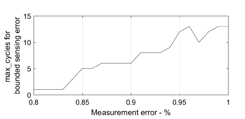
In Fig. 5 we consider the impinging EM wave of Fig. 4(b). Additionally, we assume that the power measurements of each node contain a fault expressed as a random percentage over the actual value. We are interested in deducing the minimal max_cycle value that eliminates the error via the consensus value averaging. The consensus process is shown to be very robust to such errors in the measurements. For errors up to ~ %, even one consensus cycle is enough, while ~ cycles can eliminate even the highest measurement errors.
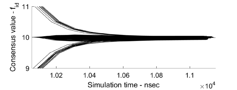
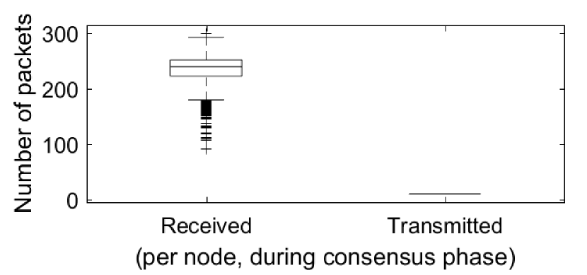
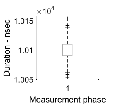
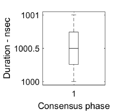
In Fig. 6-7 we focus on the % measurement error case and set max_cycles to . Fig. 6 plots the consensus (i.e., sensory) value progression versus time. For ease of exposition, we employ the EM function identifier (cf. rel. (1)) to denote the correct impinging wave attribute (). As shown, the consensus process converges rapidly even for nodes with completely erroneous initial measurement. Thus, the consensus process is economic in terms of required packet transmissions. The corresponding packet statistics are shown in Fig. 7-top: each node received packets (per cycle) from each of its neighbors, subject to some losses due to collisions. The transmission per node are strictly bounded and fully defined by the max_cycles value. Finally, as shown in Fig. 7-bottom, the measurements phase lasts for sec (i.e., RC values to iterate over, times the time to obtain a single measurement), while the consensus phase lasts for sec (i.e., max_cyles times the RD and TTW). At an aggregate EM wave sensing time of sec, ABSense shows promise for application in real-time-adapting HSFs.
V Conclusion and Future Work
The manipulation and re-shaping of EM waves via intelligent metasurfaces constitutes a key enabler of exotic capabilities in energy harvesting, medical imaging and wireless communications. Nonetheless, accurate EM manipulation requires the accurate sensing of the attributes (direction, polarization, phase) of the wave impinging on a metasurface. Filling in a gap in the related research, the study proposed a novel sensory scheme that exploits the ambient intelligence and communication capabilities of the HyperSurfaces, a novel meta-surface variant. An embedded nano-network automatically tunes the HyperSurface to full absorb the impinging waves, as exhibited by the increase of energy dissipating within it, hence indirectly estimating its attributes. The proposed scheme, validated via extensive EM simulations, can also constitute the basis for distributed EM compiler processes, were the nano-network will auto-tune the HyperSurface status to obtain any high-level objective in its macroscopic EM behavior.
In the future, the authors plan to extend the proposed scheme towards sensing non-planar, complex EM waves, while also advancing the nano-network consensus process into an always-on process that will run in parallel with EM manipulation objectives.
VI Acknowledgments
This work was funded by the European Union via the Horizon 2020: Future Emerging Topics call (FETOPEN), grant EU736876, project VISORSURF (http://www.visorsurf.eu).
The authors would like to thank all members of the VISORSURF consortium for the valuable, inter-disciplinary knowledge exchange that has taken place since the project start.
References
- [1] H. Yang et al., “A programmable metasurface with dynamic polarization, scattering and focusing control,” NPG Scientific reports, vol. 6, 2016.
- [2] H. Wakatsuchi et al., “Waveform-dependent absorbing metasurfaces,” Physical Review Letters, vol. 111, no. 24, 2013.
- [3] A. Tasolamprou and othes, “Experimental demonstration of ultrafast thz modulation in a graphene-based thin film absorber through negative photoinduced conductivity,” ACS Photonics, vol. 6, no. 3, 2019.
- [4] H. Wallace, “Analysis of rf imaging applications at frequencies over 100 ghz,” OSA Applied optics, vol. 49, no. 19, 2010.
- [5] C. Liaskos et al., “Using any surface to realize a new paradigm for wireless communications,” Communications of the ACM, vol. 61, no. 11, 2018.
- [6] A. Li et al., “Metasurfaces and their applications,” Nanophotonics, vol. 7, no. 6, 2018.
- [7] S. Abadal et al., “Computing and communications for the software-defined metamaterial paradigm: A context analysis,” IEEE Access, vol. 5, 2017.
- [8] M. electronics, “Field sensors: montena technology sa,” https://www.montena.com/system/pulse-measurement-fibre-optic-links/field-sensors/, (Accessed on 12/01/2018).
- [9] C. Liaskos et al., “Initial UML definition of the HyperSurface compiler middle-ware,” European Commission, H2020-FETOPEN-2016-2017, Project VISORSURF: Accepted Public Deliverable D2.2, 31-Dec-2017, [Online:] http://www.visorsurf.eu/m/VISORSURF-D2.2.pdf, 2017.
- [10] A. Díaz-Rubio et al., “From the generalized reflection law to the realization of perfect anomalous reflectors,” AAAS Sci. Adv., vol. 3, no. 8, 2017.
- [11] A. Tasolamprou et al., “Experimentally excellent beaming in a two-layer dielectric structure,” Opt. Express, vol. 22, no. 19, 2014.
- [12] T. Niemi et al., “Synthesis of polarization transformers,” IEEE Trans Antennas Propag, vol. 61, no. 6, 2013.
- [13] O. Tsilipakos et al., “Antimatched electromagnetic metasurfaces for broadband arbitrary phase manipulation in reflection,” ACS Photonics, vol. 5, 2018.
- [14] X. Wang et al., “Extreme asymmetry in metasurfaces via evanescent fields engineering: Angular-asymmetric absorption,” Phys Rev Lett, vol. 121, no. 25, 2018.
- [15] T. J. Cui et al., “Coding metamaterials, digital metamaterials and programmable metamaterials,” Light Sci. Appl., vol. 3, no. 10, 2014.
- [16] C. Huang et al., “Reconfigurable metasurface for multifunctional control of electromagnetic waves,” Adv. Opt. Mater., vol. 5, 2017.
- [17] F. Liu et al., “Intelligent metasurfaces with continuously tunable local surface impedance for multiple reconfigurable functions,” Phys. Rev. Appl., vol. 11, 2019.
- [18] C. Liaskos et al., “Realizing wireless communication through software-defined hypersurface environments,” in IEEE WoWMoM’18.
- [19] T. Saeed et al., “Fault adaptive routing in metasurface controller networks,” in NoCArc’18.
- [20] C. Liaskos et al., “A novel communication paradigm for high capacity and security via programmable indoor wireless environments in next generation wireless systems,” Ad Hoc Networks, vol. 87.
- [21] ——, “A new wireless communication paradigm through software-controlled metasurfaces,” IEEE Communications Magazine, vol. 56, 2018.
- [22] C. Pelzman and S.-Y. Cho, “Plasmonic metasurface for simultaneous detection of polarization and spectrum,” Opt. Lett., vol. 41, no. 6, 2016.
- [23] M. Chen et al., “Detection of orbital angular momentum with metasurface at microwave band,” IEEE Antennas Wirel. Propag. Lett., vol. 17, no. 1, 2018.
- [24] C. Hadjicostis et al., “Robust distributed average consensus via exchange of running sums,” IEEE Transactions on Automatic Control, vol. 61, no. 6, 2016.
- [25] L. Tseng and N. Vaidya, “Fault-tolerant consensus in directed graphs,” in ACM PODC’15.
- [26] N. Abuali et al., “Performance evaluation of routing protocols in electromagnetic nanonetworks,” IEEE Access, vol. 6, 2018.
- [27] A. Tsioliaridou et al., “Corona: A coordinate and routing system for nanonetworks,” in NANOCOM’15.
- [28] H. Mabed and J. Bourgeois, “A flexible medium access control protocol for dense terahertz nanonetworks,” in NANOCOM’18.
- [29] A. Tsioliaridou et al., “N3: Addressing and routing in 3d nanonetworks,” in IEEE ICT’16.
- [30] ——, “A novel protocol for network-controlled metasurfaces,” in NANOCOM’17.
- [31] F. Al-Turjman and K. I. Kilic, “Lagoon: a simple energy-aware routing protocol for wireless nano-sensor networks,” IET Wireless Sensor Systems, 2018.
- [32] C. Liaskos et al., “A deployable routing system for nanonetworks,” in IEEE ICC’16.
- [33] N. M. Estakhri, B. Edwards, and N. Engheta, “Inverse-designed metastructures that solve equations,” AAAS Science, vol. 363, no. 6433, 2019.
- [34] L. La Spada et al., “Curvilinear metasurfaces for surface wave manipulation,” Scientific reports, vol. 9, no. 1, 2019.
- [35] L. La Spada and L. Vegni, “Near-zero-index wires,” OSA Optics express, vol. 25, no. 20, 2017.
- [36] A. Vakil and N. Engheta, “Transformation optics using graphene,” AAAS Science, vol. 332, no. 6035, 2011.
- [37] A. Tasolamprou et al., “Intercell wireless communication in software-defined metasurfaces,” in ISCAS’18, 2018.
- [38] X. Timoneda et al., “Channel Characterization for Chip-scale Wireless Communications within Computing Packages,” in Proceedings of the NOCS ’18, 2018.
- [39] W. Guo et al., “Multi-scale energy harvesting,” in Wireless Information and Power Transfer: A New Paradigm for Green Communications. Springer, 2018, pp. 157–185.
- [40] CST, Microwave Studio, 2016. [Online]. Available: http://www.cst.com/
- [41] XJ Technologies, The AnyLogic Simulator, 2018. [Online]. Available: http://www.anylogic.com/
- [42] A. Tsioliaridou et al., “Stateless linear-path routing for 3d nanonetworks,” in ACM NANOCOM’16.
- [43] A. Iyer et al., “What is the right model for wireless channel interference?” IEEE Trans. Wir. Comm., vol. 8, no. 5, 2009.