AWG-based Nonblocking Shuffle-Exchange Networks

Tong Ye,  Jingjie Ding, Tony T. Lee,  and Guido Maier This work was supported by the National Science Foundation of China (61571288, 61671286, and 61433009).Tong Ye, Jingjie Ding are with the State Key Laboratory of Advanced Optical Communication Systems and Networks, Shanghai Jiao Tong University, Shanghai 200240, China. (email: {yetong,mrdingjay}@sjtu.edu.cn).Tony T. Lee is with the Chinese University of Hong Kong (Shenzhen), Shenzhen 518172, China (e-mail: tonylee@cuhk.edu.cn). Guido Maier is with the Dipartimento di Elettronica, Informazione e Bioingegneria, Politecnico di Milano, Milan 20133, Italy (e-mail: guido.maier@polimi.it).
Abstract

Optical shuffle-exchange networks (SENs) have wide application in different kinds of interconnection networks. This paper proposes an approach to construct modular optical SENs, using a set of arrayed waveguide gratings (AWGs) and tunable wavelength converters (TWCs). According to the wavelength routing property of AWGs, we demonstrate for the first time that an AWG is functionally equivalent to a classical shuffle network by nature. Based on this result, we devise a systematic method to design a large-scale wavelength-division-multiplexing (WDM) shuffle network using a set of small-size AWGs associated with the same wavelength set. Combining the AWG-based WDM shuffle networks and the TWCs with small conversion range, we finally obtain an AWG-based WDM SEN, which not only is scalable in several ways, but also can achieve 100% utilization when the input wavelength channels are all busy. We also study the routing and wavelength assignment (RWA) problem of the AWG-based WDM SEN, and prove that the self-routing property and the nonblocking routing conditions of classical SENs are preserved in such AWG-based WDM SEN.

Index Terms:
Shuffle-exchange network (SEN), routing and wavelength assignment (RWA), arrayed-waveguide grating (AWG), wavelength division multiplexing (WDM).a’da’d’s

I Introduction

With the coming of big data era, high-speed switching networks become more and more important. Currently, massive data exchange is very common within the information systems at different scales. On a multi-processor system, different processors work together through a switching network to provide high-power data processing capability [1, 2, 3]. This is also true for mega data centers, where more than 105superscript10510^{5} servers [4] are interconnected via a large-scale switching network to deliver high-quality cloud computing service or high-performance computation service. Also, in an even larger area, high-capacity switching network is now indispensable to big data transfers among different data centers [5]. For example, it is reported that the traffic rate per link in a data center has come to tens of Tb/s [5, 6], and will reach Pb/s in the near future [4, 5, 7].

In the meanwhile, optical shuffle-exchange networks (SENs) have exhibited several advantages in high-speed interconnection [8]. First, as a kind of optical switches, an optical SEN can provide large switching capacity [4, 9, 10, 11], especially when it employs wavelength division multiplexing (WDM) technology [12]. Second, the structure of SENs is very regular and thus easy to deploy [4, 13]. Third, the SEN has a less network diameter than other networks, and thus less implementation cost [3]. Fourth, the routing algorithm of the SEN is simple since it has a self-routing property [14, 15]: the path between an input-output pair is uniquely determined by the addresses of the input and the output. Hence, optical SEN has been considered as a promising candidate to provide high-speed interconnection for different network application scenarios [1, 2, 4, 8, 16].
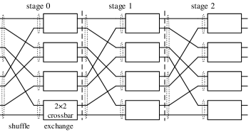
Refer to caption
Figure 1: An 8×8888\times 8 shuffle exchange network.

The SEN is a kind of multi-stage switching networks, as Fig. 1 illustrates. An mn×mnsuperscript𝑚𝑛superscript𝑚𝑛{m^{n}}\times{m^{n}} SEN consists of n𝑛n cascaded switching stages, each of which is a shuffle network followed by an exchange network. For example, the SEN in Fig. 1 is a SEN with m=2𝑚2m=2 and n=3𝑛3n=3. Each shuffle network is an mn×mnsuperscript𝑚𝑛superscript𝑚𝑛m^{n}\times m^{n} perfect shuffle. It splits its inputs and its outputs into m𝑚m input groups and mn1superscript𝑚𝑛1m^{n-1} output groups, respectively, and connects an input group and an output group via one and only one link. Each exchange network contains mn1superscript𝑚𝑛1m^{n-1} m×m𝑚𝑚m\times m crossbars, and each crossbar is attached to an output group of the shuffle network. In other words, each crossbar performs switching function for an output group. For example, each shuffle network in Fig. 1 is a 23×23superscript23superscript232^{3}\times 2^{3} perfect shuffle, and it partitions 8 inputs and 8 outputs into m=2𝑚2m=2 input groups and mn1=231=4superscript𝑚𝑛1superscript2314m^{n-1}=2^{3-1}=4 output groups, each of which is encircled by a dotted circle. Each exchange network in Fig. 1 consists of mn1=231=4superscript𝑚𝑛1superscript2314m^{n-1}=2^{3-1}=4 2×2222\times 2 crossbars, and the inputs of a crossbar are actually the outputs of an output group of a shuffle network.

Though electrical SEN is already a mature technology, the design of scalable optical SENs remains a big challenge. Up to now, several kinds of optical components, such as micro-electromechanical system (MEMS) [4], arrayed waveguide grating (AWG) [17], and tunable wavelength converter (TWC) [18], have been available to construct optical switches. The power consumption of optical components typically increases with their size, which, however, cannot be very large, due to cost, synthesis difficulty, or physical-layer performance. For example, an AWG with a large port count induces serious coherent crosstalk when the same wavelength is fed into a number of inputs [19]. Such coherent crosstalk causes signal degradation and is very hard to get rid of. Another example is TWC with large wavelength conversion range, which is powerful but expensive [20]. Also, the number of wavelengths required by the network, referred to as wavelength granularity in this paper, should not be very large, since the number of wavelengths available in optical transmission window is limited [21]. Furthermore, the number of links in each shuffle network should be carefully considered. It is well-known that the cabling complexity has become one of the development bottle-neck of high-speed switching nodes [22]. At last, the optical SEN should be compact and easy for maintenance, which is also very important for practical applications. Though there exist several optical designs, they cannot meet all these requirements at the same time.

I-A Previous work

In the early phase, the design of optical SENs was mainly based on free-space optics (FSO) technology. Ref. [23, 24, 25] proposed several designs, employing customized complex lens, polarizing beam splitters and micro-blazed grating arrays. In [26, 27, 13], different kinds of exchange networks were implemented with spatial light modulators, ferroelectric liquid crystals, calcite crystals, and arrayed optical switches, respectively. However, these FSO devices are typically costly, bulky, and difficult to adjust and maintain [28]. Therefore, the FSO-based schemes are not suitable for most of practical applications.

In [9] and [29], two kinds of fiber-based SENs were proposed to avoid the disadvantages of the FSO-based SEN. In such SENs, optical fiber was used to construct the optical shuffle networks, while the MEMSs [29] or the electric-optical switches [9] were employed to implement the optical exchange networks. One feature of such kind of SENs is that each fiber only carries one optical signal. Thus, there are N𝑁N fibers in each optical shuffle network if the port count of the SEN is N𝑁N. Clearly, the cabling complexity of optical shuffle networks in the SEN will be high if N𝑁N is large.

Recently, combination of AWGs and TWCs provides a new way to construct SENs [17]. An N×N𝑁𝑁N\times N AWG is an N×N𝑁𝑁N\times N passive optical component [17], each port of which carries the same set of N𝑁N wavelengths. The function of AWGs is to forward the signal from an input to an output without any contention. On the other hand, the TWC can convert an input wavelength to any of the output wavelengths in the conversion range. With the TWCs at each input, the AWG can perform high-speed switching function [17, 30, 31, 32, 33, 34, 35]. In particular, a TWC can send an optical packet from an input to an output of the AWG, if it converts the incoming wavelength to one of N𝑁N wavelengths. Based on such feature, Ref. [17] proposed an N×N𝑁𝑁N\times N AWG-based SEN with log2Nsubscript2𝑁\log_{2}N cascaded switching stages, each of which was an N×N𝑁𝑁N\times N AWG with each output attached by a TWC. However, the design in [17] has several drawbacks as follows. Firstly, in order to eliminate coherent crosstalk, the AWG-based SEN in [17] does not make full use of the WDM property of AWGs. Only N𝑁N wavelength channels of each AWG are employed, and thus the AWG utilization is only 1/N1𝑁1/N. Secondly, when N𝑁N is large, the scalability of this design is not good due to the following reasons: 1) it needs large-scale AWGs, which results in large wavelength granularity; 2) the conversion range of the employed TWCs is large; 3) a complex interconnection between the TWCs and the AWG at each stage is required to avoid the coherent crosstalk induced by the large-scale AWG.

I-B Our Work

The focus of this paper is on the construction of AWG-based WDM SENs. Different from that in [17], the design of this paper takes full advantage of the WDM property of AWGs, such that the above-mentioned drawbacks can be avoided.

To achieve this goal, the important step is to construct a modular AWG-based WDM shuffle network, in which the wavelength channels of each AWG are fully utilized. We demonstrate that an AWG is functionally equivalent to a shuffle network by nature if the wavelength channels at each port are considered as a channel group. Based on this result, we devise a systematic method to construct a large-scale WDM shuffle network using a collection of small-size AWGs associated with the same wavelength set. We show that the cabling complexity of such modular AWG-based shuffle networks is remarkably cut down and serious coherent crosstalk is suppressed.

We then propose an AWG-based WDM SEN by combining AWG-based WDM shuffle networks and TWC modules, each of which is constructed from a set of TWCs. We show that the conversion range of TWCs in the network is reduced since the size of each employed AWG is small. We also study the routing and wavelength assignment (RWA) problem of the AWG-based WDM SEN. We show that the self-routing property and the nonblocking routing conditions of the classical SEN are also preserved in such AWG-based WDM SEN.

In summary, our main contribution includes:

  1. 1)

    We find, for the first time, the functional equivalence between a single AWG and a shuffle network;

  2. 2)

    We develop a systematic method to construct modular AWG-based shuffle networks, of which the AWG size, the wavelength granularity, and the cabling complexity are scaled down;

  3. 3)

    We design AWG-based WDM SENs, of which the coherent crosstalk is small and the utilization of the optical components is 100% if the input channels are all busy.

The rest of this paper is organized as follows. We first demonstrate the functional equivalence between an AWG and a shuffle network in Section II, and then we develop a systematic approach to construct a modular AWG-based WDM shuffle network in Section III. Based on the result in Section III, we design AWG-based WDM SENs in Section IV. At last, Section V shows that the self-routing property and the nonblocking conditions of classical SENs are also preserved by such WDM SENs. Finally, Section VI concludes this paper.

II Generalized AWG-Based Shuffle Network

AWG is a kind of passive wavelength router, which is able to provide exact one connection between each input and each output. Because of such unique feature, the AWG has been used to provide broadband optical interconnections for different applications, such as shuffle network in [17]. However, the efficient way for AWGs to fulfill the function of shuffle networks is still unknown.

In this section, we show for the first time that an AWG is functionally equivalent to a shuffle network. In particular, we first recall the definition of shuffle networks in Section II-A, and then demonstrate why and how the AWG can be equivalent to a shuffle network in Section II-B.

II-A Generalized Shuffle Network

Refer to caption
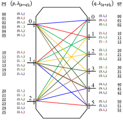
Figure 2: An example of 18×18181818\times 18 generalized shuffle 𝒩(3,6)𝒩36\mathcal{N}(3,6).

Consider an N×N𝑁𝑁N\times N interconnection network with N𝑁N inputs and N𝑁N outputs. Assume that N𝑁N inputs can be equally divided into m𝑚m groups, each with l𝑙l ports, and N𝑁N outputs can be partitioned into l𝑙l groups, each with m𝑚m ports, where N=ml𝑁𝑚𝑙N=ml. The N×N𝑁𝑁N\times N generalized shuffle network can be defined as follows.

Definition 1.

An N×N𝑁𝑁N\times N interconnection network is an N×N𝑁𝑁N\times N generalized shuffle network, denoted by 𝒩(m,l)𝒩𝑚𝑙\mathcal{N}(m,l), if the q𝑞qth port of the p𝑝pth input group connects to the p𝑝pth port of the q𝑞qth output group, where p=0,1,,m1𝑝01𝑚1p=0,1,\cdots,m-1 and q=0,1,,l1𝑞01𝑙1q=0,1,\cdots,l-1.

Fig. 2 plots an 18×18181818\times 18 shuffle network 𝒩(3,6)𝒩36\mathcal{N}(3,6), where 18 inputs and 18 outputs are evenly divided into 3 groups and 6 groups, respectively. Also, the 5th input of input group 0 connects with the 0th output of output group 5.

We assign each port a two-field address, of which the first field is called group field while the second field is port field. In particular, we assign a two-field address p¯q¯¯absent𝑝¯absent𝑞\underaccent{{\underline{\mskip 7.0mu}}}{p}\underaccent{{\underline{\mskip 7.0mu}}}{q} to the q𝑞qth input of the p𝑝pth input group, and a two-field address q¯p¯¯absent𝑞¯absent𝑝\underaccent{{\underline{\mskip 7.0mu}}}{q}\underaccent{{\underline{\mskip 7.0mu}}}{p} to the p𝑝pth output of the q𝑞qth output group, where the underlined numbers in the field address are used to represent the corresponding port and/or group sub-addresses. Under such numbering scheme, input p¯q¯¯absent𝑝¯absent𝑞\underaccent{{\underline{\mskip 7.0mu}}}{p}\underaccent{{\underline{\mskip 7.0mu}}}{q} connects with output q¯p¯¯absent𝑞¯absent𝑝\underaccent{{\underline{\mskip 7.0mu}}}{q}\underaccent{{\underline{\mskip 7.0mu}}}{p}. We thus denote this connection by C(p¯q¯,q¯p¯)𝐶¯absent𝑝¯absent𝑞¯absent𝑞¯absent𝑝C(\underaccent{{\underline{\mskip 7.0mu}}}{p}\underaccent{{\underline{\mskip 7.0mu}}}{q},\underaccent{{\underline{\mskip 7.0mu}}}{q}\underaccent{{\underline{\mskip 7.0mu}}}{p}). For example, input 1¯4¯¯absent1¯absent4\underaccent{{\underline{\mskip 7.0mu}}}{1}\underaccent{{\underline{\mskip 7.0mu}}}{4} connects with output 4¯1¯¯absent4¯absent1\underaccent{{\underline{\mskip 7.0mu}}}{4}\underaccent{{\underline{\mskip 7.0mu}}}{1} via connection C(1¯4¯,4¯1¯)𝐶¯absent1¯absent4¯absent4¯absent1C(\underaccent{{\underline{\mskip 7.0mu}}}{1}\underaccent{{\underline{\mskip 7.0mu}}}{4},\underaccent{{\underline{\mskip 7.0mu}}}{4}\underaccent{{\underline{\mskip 7.0mu}}}{1}) in Fig. 2.

From the above definition, it is easy to show that shuffle networks have the following two features:

  1. F1.

    An input group connects with an output group via exact one connection;

  2. F2.

    An input connects to an output, whose address is formed by exchanging the two sub-addresses of the input address.

An N×N𝑁𝑁N\times N interconnection network is functionally equivalent to shuffle network 𝒩(m,l)𝒩𝑚𝑙\mathcal{N}(m,l) if it can fulfill these two connection features.

II-B Single-AWG based Shuffle Network

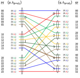
An m×l𝑚𝑙m\times l AWG, denoted as 𝒜(m,l)𝒜𝑚𝑙\mathcal{A}(m,l), has m𝑚m inputs and l𝑙l outputs, which are labelled from top to bottom. AWG 𝒜(m,l)𝒜𝑚𝑙\mathcal{A}(m,l) is associated with a wavelength set Λ={λ0,λ1,,λ|Λ|1}Λsubscript𝜆0subscript𝜆1subscript𝜆Λ1\Lambda=\{\lambda_{0},\lambda_{1},\cdots,\lambda_{|\Lambda|-1}\} in a free spectrum range (FSR), where |Λ|=max{m,l}Λmax𝑚𝑙|\Lambda|=\mbox{max}\{m,l\}. Without loss of generality, we assume that l>m𝑙𝑚l>m in this section, and thus |Λ|=lΛ𝑙|\Lambda|=l. This paper only considers the wavelength channels in the main FSR, because AWGs suffer physical performance degradation at the wavelength channels outside the main FSR [36]. In the main FSR, each input of AWG 𝒜(m,l)𝒜𝑚𝑙\mathcal{A}(m,l) carries l𝑙l wavelength channels, and each output has m𝑚m wavelength channels. Fig. 3 gives an example of a 3×6363\times 6 AWG 𝒜(3,6)𝒜36\mathcal{A}(3,6).

Refer to caption
Refer to caption
Figure 3: Equivalence between a single AWG and a shuffle: (a) AWG 𝒜(3,6)𝒜36\mathcal{A}(3,6) and (b) its space representation.

The AWG is a passive wavelength router. In an m×l𝑚𝑙m\times l AWG, input p𝑝p is connected to output q𝑞q via wavelength λisubscript𝜆𝑖\lambda_{i}, where:

i=[p+q]l𝑖subscriptdelimited-[]𝑝𝑞𝑙{i=[p+q]_{l}} (1)

or

q=[ip]l𝑞subscriptdelimited-[]𝑖𝑝𝑙{q=[i-p]_{l}} (2)

or

p=[iq]l,𝑝subscriptdelimited-[]𝑖𝑞𝑙{p=[i-q]_{l},} (3)

where [X]l(X mod l)subscriptdelimited-[]𝑋𝑙𝑋 mod 𝑙[X]_{l}\triangleq(X\mbox{ mod }l). The wavelength routing property (1) clearly shows that input p𝑝p and output q𝑞q are connected by exact one wavelength channel λ[p+q]lsubscript𝜆subscriptdelimited-[]𝑝𝑞𝑙\lambda_{[p+q]_{l}}, of which the connection is denoted by C~A(p,q,λ[p+q]l)subscript~𝐶𝐴𝑝𝑞subscript𝜆subscriptdelimited-[]𝑝𝑞𝑙\tilde{C}_{A}(p,q,\lambda_{[p+q]_{l}}). Such connection feature is consistent with the feature F1 of shuffle network 𝒩(m,l)𝒩𝑚𝑙\mathcal{N}(m,l).

TABLE I: Wavelength Routing Table 𝑻Asubscript𝑻𝐴\bm{T}_{A} of a 3×6363\times 6 AWG 𝒜(3,6)𝒜36\mathcal{A}(3,6)
p\q\𝑝𝑞p\backslash q 00 111 222 333 444 555
00 λ0subscript𝜆0\lambda_{0} λ1subscript𝜆1\lambda_{1} λ2subscript𝜆2\lambda_{2} λ3subscript𝜆3\lambda_{3} λ4subscript𝜆4\lambda_{4} λ5subscript𝜆5\lambda_{5}
111 λ1subscript𝜆1\lambda_{1} λ2subscript𝜆2\lambda_{2} λ3subscript𝜆3\lambda_{3} λ4subscript𝜆4\lambda_{4} λ5subscript𝜆5\lambda_{5} λ0subscript𝜆0\lambda_{0}
222 λ2subscript𝜆2\lambda_{2} λ3subscript𝜆3\lambda_{3} λ4subscript𝜆4\lambda_{4} λ5subscript𝜆5\lambda_{5} λ0subscript𝜆0\lambda_{0} λ1subscript𝜆1\lambda_{1}

Also, the wavelength routing property (1) of 𝒜(m,l)𝒜𝑚𝑙\mathcal{A}(m,l) can be described by an m×l𝑚𝑙m\times l routing table, denoted by 𝑻Asubscript𝑻𝐴\bm{T}_{A}, where the p𝑝pth row and the q𝑞qth column are corresponding to input p𝑝p and output q𝑞q, and the entry at the intersection, denoted by (p,q)𝑝𝑞(p,q), records the wavelength channel λ[p+q]lsubscript𝜆subscriptdelimited-[]𝑝𝑞𝑙\lambda_{[p+q]_{l}} of connection C~A(p,q,λ[p+q]l)subscript~𝐶𝐴𝑝𝑞subscript𝜆subscriptdelimited-[]𝑝𝑞𝑙\tilde{C}_{A}(p,q,\lambda_{[p+q]_{l}}). For example, Table I is the routing table of AWG 𝒜(3,6)𝒜36\mathcal{A}(3,6) in Fig. 3, and entry (1,4)14(1,4) is the wavelength channel λ[p+q]l=λ[1+4]6=λ5subscript𝜆subscriptdelimited-[]𝑝𝑞𝑙subscript𝜆subscriptdelimited-[]146subscript𝜆5\lambda_{[p+q]_{l}}=\lambda_{[1+4]_{6}}=\lambda_{5} of C~(1,4,λ5)~𝐶14subscript𝜆5\tilde{C}(1,4,\lambda_{5}). Therefore, the entries at row p𝑝p (column q𝑞q) are corresponding to the wavelength channels at input p𝑝p (output q𝑞q).

According to the structure of 𝑻Asubscript𝑻𝐴\bm{T}_{A}, we assign addresses to the input channels and the output channels as follows:

  1. 1)

    Input channel: Assign addresses to the wavelength channels at row p𝑝p (i.e., input group p𝑝p) from left to right. The q𝑞qth entry at row p𝑝p is assigned with field address p¯q¯¯absent𝑝¯absent𝑞\underaccent{{\underline{\mskip 7.0mu}}}{p}\underaccent{{\underline{\mskip 7.0mu}}}{q} and two-tuple address (p,λ[p+q]l)𝑝subscript𝜆subscriptdelimited-[]𝑝𝑞𝑙(p,\lambda_{[p+q]_{l}}).

  2. 2)

    Output channel: Assign addresses to the wavelength channels at column q𝑞q (i.e., output group q𝑞q) from top to bottom. The p𝑝pth entry at column q𝑞q is assigned with field address q¯p¯¯absent𝑞¯absent𝑝\underaccent{{\underline{\mskip 7.0mu}}}{q}\underaccent{{\underline{\mskip 7.0mu}}}{p} and two-tuple address (q,λ[q+p]l)𝑞subscript𝜆subscriptdelimited-[]𝑞𝑝𝑙(q,\lambda_{[q+p]_{l}}).

In the field address, the first field is called port field, and the second field is referred to as channel field.

With such numbering scheme, entry (p,q)𝑝𝑞(p,q) in 𝑻Asubscript𝑻𝐴\bm{T}_{A} delineates both input channel p¯q¯¯absent𝑝¯absent𝑞\underaccent{{\underline{\mskip 7.0mu}}}{p}\underaccent{{\underline{\mskip 7.0mu}}}{q} and output channel q¯p¯¯absent𝑞¯absent𝑝\underaccent{{\underline{\mskip 7.0mu}}}{q}\underaccent{{\underline{\mskip 7.0mu}}}{p}, which means they connect to each other through λ[p+q]lsubscript𝜆subscriptdelimited-[]𝑝𝑞𝑙\lambda_{[p+q]_{l}}. To describe such kind of connectivity explicitly, we replace entry (p,q)𝑝𝑞(p,q) in 𝑻Asubscript𝑻𝐴\bm{T}_{A} with input channel p¯q¯¯absent𝑝¯absent𝑞\underaccent{{\underline{\mskip 7.0mu}}}{p}\underaccent{{\underline{\mskip 7.0mu}}}{q} and output channel q¯p¯¯absent𝑞¯absent𝑝\underaccent{{\underline{\mskip 7.0mu}}}{q}\underaccent{{\underline{\mskip 7.0mu}}}{p}, and obtain a new table, called connectivity table and denoted by 𝑻Bsubscript𝑻𝐵\bm{T}_{B}. For example, Table II gives the connectivity table of 𝒜(3,6)𝒜36\mathcal{A}(3,6), in which entry (1,4)14(1,4) shows that input channel 1¯4¯¯absent1¯absent4\underaccent{{\underline{\mskip 7.0mu}}}{1}\underaccent{{\underline{\mskip 7.0mu}}}{4} connects with output channel 4¯1¯¯absent4¯absent1\underaccent{{\underline{\mskip 7.0mu}}}{4}\underaccent{{\underline{\mskip 7.0mu}}}{1}. This property is quite similar to the connection feature F2 of shuffle network 𝒩(m,l)𝒩𝑚𝑙\mathcal{N}(m,l).

TABLE II: Connectivity Table 𝑻Bsubscript𝑻𝐵\bm{T}_{B} of 𝒜(3,6)𝒜36\mathcal{A}(3,6)
p\q\𝑝𝑞p\backslash q 00 111 222 333 444 555
00 0¯0¯,0¯0¯¯absent0¯absent0¯absent0¯absent0\underaccent{{\underline{\mskip 7.0mu}}}{0}\underaccent{{\underline{\mskip 7.0mu}}}{0},\underaccent{{\underline{\mskip 7.0mu}}}{0}\underaccent{{\underline{\mskip 7.0mu}}}{0} 0¯1¯,1¯0¯¯absent0¯absent1¯absent1¯absent0\underaccent{{\underline{\mskip 7.0mu}}}{0}\underaccent{{\underline{\mskip 7.0mu}}}{1},\underaccent{{\underline{\mskip 7.0mu}}}{1}\underaccent{{\underline{\mskip 7.0mu}}}{0} 0¯2¯,2¯0¯¯absent0¯absent2¯absent2¯absent0\underaccent{{\underline{\mskip 7.0mu}}}{0}\underaccent{{\underline{\mskip 7.0mu}}}{2},\underaccent{{\underline{\mskip 7.0mu}}}{2}\underaccent{{\underline{\mskip 7.0mu}}}{0} 0¯3¯,3¯0¯¯absent0¯absent3¯absent3¯absent0\underaccent{{\underline{\mskip 7.0mu}}}{0}\underaccent{{\underline{\mskip 7.0mu}}}{3},\underaccent{{\underline{\mskip 7.0mu}}}{3}\underaccent{{\underline{\mskip 7.0mu}}}{0} 0¯4¯,4¯0¯¯absent0¯absent4¯absent4¯absent0\underaccent{{\underline{\mskip 7.0mu}}}{0}\underaccent{{\underline{\mskip 7.0mu}}}{4},\underaccent{{\underline{\mskip 7.0mu}}}{4}\underaccent{{\underline{\mskip 7.0mu}}}{0} 0¯5¯,5¯0¯¯absent0¯absent5¯absent5¯absent0\underaccent{{\underline{\mskip 7.0mu}}}{0}\underaccent{{\underline{\mskip 7.0mu}}}{5},\underaccent{{\underline{\mskip 7.0mu}}}{5}\underaccent{{\underline{\mskip 7.0mu}}}{0}
111 1¯0¯,0¯1¯¯absent1¯absent0¯absent0¯absent1\underaccent{{\underline{\mskip 7.0mu}}}{1}\underaccent{{\underline{\mskip 7.0mu}}}{0},\underaccent{{\underline{\mskip 7.0mu}}}{0}\underaccent{{\underline{\mskip 7.0mu}}}{1} 1¯1¯,1¯1¯¯absent1¯absent1¯absent1¯absent1\underaccent{{\underline{\mskip 7.0mu}}}{1}\underaccent{{\underline{\mskip 7.0mu}}}{1},\underaccent{{\underline{\mskip 7.0mu}}}{1}\underaccent{{\underline{\mskip 7.0mu}}}{1} 1¯2¯,2¯1¯¯absent1¯absent2¯absent2¯absent1\underaccent{{\underline{\mskip 7.0mu}}}{1}\underaccent{{\underline{\mskip 7.0mu}}}{2},\underaccent{{\underline{\mskip 7.0mu}}}{2}\underaccent{{\underline{\mskip 7.0mu}}}{1} 1¯3¯,3¯1¯¯absent1¯absent3¯absent3¯absent1\underaccent{{\underline{\mskip 7.0mu}}}{1}\underaccent{{\underline{\mskip 7.0mu}}}{3},\underaccent{{\underline{\mskip 7.0mu}}}{3}\underaccent{{\underline{\mskip 7.0mu}}}{1} 1¯4¯,4¯1¯¯absent1¯absent4¯absent4¯absent1\underaccent{{\underline{\mskip 7.0mu}}}{1}\underaccent{{\underline{\mskip 7.0mu}}}{4},\underaccent{{\underline{\mskip 7.0mu}}}{4}\underaccent{{\underline{\mskip 7.0mu}}}{1} 1¯5¯,5¯1¯¯absent1¯absent5¯absent5¯absent1\underaccent{{\underline{\mskip 7.0mu}}}{1}\underaccent{{\underline{\mskip 7.0mu}}}{5},\underaccent{{\underline{\mskip 7.0mu}}}{5}\underaccent{{\underline{\mskip 7.0mu}}}{1}
222 2¯0¯,0¯2¯¯absent2¯absent0¯absent0¯absent2\underaccent{{\underline{\mskip 7.0mu}}}{2}\underaccent{{\underline{\mskip 7.0mu}}}{0},\underaccent{{\underline{\mskip 7.0mu}}}{0}\underaccent{{\underline{\mskip 7.0mu}}}{2} 2¯1¯,1¯2¯¯absent2¯absent1¯absent1¯absent2\underaccent{{\underline{\mskip 7.0mu}}}{2}\underaccent{{\underline{\mskip 7.0mu}}}{1},\underaccent{{\underline{\mskip 7.0mu}}}{1}\underaccent{{\underline{\mskip 7.0mu}}}{2} 2¯2¯,2¯2¯¯absent2¯absent2¯absent2¯absent2\underaccent{{\underline{\mskip 7.0mu}}}{2}\underaccent{{\underline{\mskip 7.0mu}}}{2},\underaccent{{\underline{\mskip 7.0mu}}}{2}\underaccent{{\underline{\mskip 7.0mu}}}{2} 2¯3¯,3¯2¯¯absent2¯absent3¯absent3¯absent2\underaccent{{\underline{\mskip 7.0mu}}}{2}\underaccent{{\underline{\mskip 7.0mu}}}{3},\underaccent{{\underline{\mskip 7.0mu}}}{3}\underaccent{{\underline{\mskip 7.0mu}}}{2} 2¯4¯,4¯2¯¯absent2¯absent4¯absent4¯absent2\underaccent{{\underline{\mskip 7.0mu}}}{2}\underaccent{{\underline{\mskip 7.0mu}}}{4},\underaccent{{\underline{\mskip 7.0mu}}}{4}\underaccent{{\underline{\mskip 7.0mu}}}{2} 2¯5¯,5¯2¯¯absent2¯absent5¯absent5¯absent2\underaccent{{\underline{\mskip 7.0mu}}}{2}\underaccent{{\underline{\mskip 7.0mu}}}{5},\underaccent{{\underline{\mskip 7.0mu}}}{5}\underaccent{{\underline{\mskip 7.0mu}}}{2}

Therefore, if the channels at one port are regarded as a channel group, 𝒜(m,l)𝒜𝑚𝑙\mathcal{A}(m,l) and 𝒩(m,l)𝒩𝑚𝑙\mathcal{N}(m,l) have the following equivalence:

Property 1.

A single AWG 𝒜(m,l)𝒜𝑚𝑙\mathcal{A}(m,l) is equivalent to a shuffle network 𝒩(m,l)𝒩𝑚𝑙\mathcal{N}(m,l) in terms of the connectivity between input channels and output channels.

Proof:

This property holds due to the fact that each input-output pair of 𝒜(m,l)𝒜𝑚𝑙\mathcal{A}(m,l) is connected via only one wavelength channel, which is elaborated as follows:

  1. 1)

    In 𝒜(m,l)𝒜𝑚𝑙\mathcal{A}(m,l), input p𝑝p connects to output q𝑞q via only one connection C~A(p,q,λ[p+q]l)subscript~𝐶𝐴𝑝𝑞subscript𝜆subscriptdelimited-[]𝑝𝑞𝑙\tilde{C}_{A}(p,q,\lambda_{[p+q]_{l}}). It follows that there exists an one-one and onto mapping

    p,qC~A(p,q,λ[p+q]l).𝑝𝑞subscript~𝐶𝐴𝑝𝑞subscript𝜆subscriptdelimited-[]𝑝𝑞𝑙{p,q\leftrightarrow\tilde{C}_{A}(p,q,\lambda_{[p+q]_{l}}).} (4)
  2. 2)

    According to the property of shuffle network 𝒩(m,l)𝒩𝑚𝑙\mathcal{N}(m,l), input group p𝑝p is connected to output group q𝑞q via a unique connection C(p¯q¯,q¯p¯)𝐶¯absent𝑝¯absent𝑞¯absent𝑞¯absent𝑝C(\underaccent{{\underline{\mskip 7.0mu}}}{p}\underaccent{{\underline{\mskip 7.0mu}}}{q},\underaccent{{\underline{\mskip 7.0mu}}}{q}\underaccent{{\underline{\mskip 7.0mu}}}{p}). Thus, there is an one-one and onto mapping

    p,qC(p¯q¯,q¯p¯).𝑝𝑞𝐶¯absent𝑝¯absent𝑞¯absent𝑞¯absent𝑝{p,q\leftrightarrow C(\underaccent{{\underline{\mskip 7.0mu}}}{p}\underaccent{{\underline{\mskip 7.0mu}}}{q},\underaccent{{\underline{\mskip 7.0mu}}}{q}\underaccent{{\underline{\mskip 7.0mu}}}{p}).} (5)

Thus, if each port of 𝒜(m,l)𝒜𝑚𝑙\mathcal{A}(m,l) is regarded as a channel group, there is an one-one and onto mapping between connection C~A(p,q,λ[p+q]l)subscript~𝐶𝐴𝑝𝑞subscript𝜆subscriptdelimited-[]𝑝𝑞𝑙\tilde{C}_{A}(p,q,\lambda_{[p+q]_{l}}) in 𝒜(m,l)𝒜𝑚𝑙\mathcal{A}(m,l) and connection C(p¯q¯,q¯p¯)𝐶¯absent𝑝¯absent𝑞¯absent𝑞¯absent𝑝C(\underaccent{{\underline{\mskip 7.0mu}}}{p}\underaccent{{\underline{\mskip 7.0mu}}}{q},\underaccent{{\underline{\mskip 7.0mu}}}{q}\underaccent{{\underline{\mskip 7.0mu}}}{p}) in 𝒩(m,l)𝒩𝑚𝑙\mathcal{N}(m,l), i.e.,

C~A(p,q,λ[p+q]l)C(p¯q¯,q¯p¯).subscript~𝐶𝐴𝑝𝑞subscript𝜆subscriptdelimited-[]𝑝𝑞𝑙𝐶¯absent𝑝¯absent𝑞¯absent𝑞¯absent𝑝{\tilde{C}_{A}(p,q,\lambda_{[p+q]_{l}})\leftrightarrow C(\underaccent{{\underline{\mskip 7.0mu}}}{p}\underaccent{{\underline{\mskip 7.0mu}}}{q},\underaccent{{\underline{\mskip 7.0mu}}}{q}\underaccent{{\underline{\mskip 7.0mu}}}{p}).} (6)

This establishes Property 1. ∎

The space representation of 𝒜(m,l)𝒜𝑚𝑙\mathcal{A}(m,l) is plotted in Fig. 3, where each line in the left side represents an input channel, each line in the right side stands for an output channel, and that in between is a connection connecting a pair of input channel and output channel. Fig. 3 clearly shows the one-one and onto mapping between the connection in 𝒜(m,l)𝒜𝑚𝑙\mathcal{A}(m,l) and that in 𝒩(m,l)𝒩𝑚𝑙\mathcal{N}(m,l).

According to Property 1, we can use an m×l𝑚𝑙m\times l AWG to construct an N×N𝑁𝑁N\times N single-AWG based shuffle network 𝒜(m,l)𝒜𝑚𝑙\mathcal{A}(m,l), where N=ml𝑁𝑚𝑙N=ml. The cabling complexity is only O(l)𝑂𝑙O(l), since we need m+l𝑚𝑙m+l fibers at the inputs and outputs when we use it. Also, the m×l𝑚𝑙m\times l AWG contains N=ml𝑁𝑚𝑙N=ml wavelength channels, and thus the utilization of the AWG is 100% if all the input wavelength channels are busy. However, as either the number of inputs m𝑚m or that of outputs l𝑙l becomes large, the single-AWG based shuffle network is not scalable and will suffer from difficult synthesis technique, serious crosstalk, and large wavelength granularity, as we mention in Section I.

III Modular AWG-based Shuffle Network

In this section, we study the method to construct a modular AWG-based shuffle network, which is the key step for the design of AWG-based SENs. In particular, we consider how to devise 𝒩(m,l)𝒩𝑚𝑙\mathcal{N}(m,l) using a set of r𝑟r m×m𝑚𝑚m\times m AWGs, where l=rm𝑙𝑟𝑚l=rm and r=1,2,3,𝑟123r=1,2,3,\cdots. From Section II, we establish the equivalence between a single AWG and a shuffle network through investigating the routing table of AWGs. Thus, Section III-A starts the construction from the design of the routing table of the modular AWG-based shuffle network, based on which we come up with a systematic method to achieve the construction in Section III-B.

III-A Routing Table of 𝒲(m,rm)𝒲𝑚𝑟𝑚\mathcal{W}(m,rm)

We denote the modular AWG-based shuffle network to be constructed as 𝒲(m,rm)𝒲𝑚𝑟𝑚\mathcal{W}(m,rm). In 𝒲(m,rm)𝒲𝑚𝑟𝑚\mathcal{W}(m,rm), there are mrm=rm2𝑚𝑟𝑚𝑟superscript𝑚2m\cdot rm=rm^{2} input wavelength channels and rm2𝑟superscript𝑚2rm^{2} output wavelength channels. These rm2𝑟superscript𝑚2rm^{2} input channels are divided into m𝑚m input groups, each with rm𝑟𝑚rm input channels, and rm2𝑟superscript𝑚2rm^{2} output channels are divided into rm𝑟𝑚rm output groups, each with m𝑚m output channels.

Since the building blocks of 𝒲(m,rm)𝒲𝑚𝑟𝑚\mathcal{W}(m,rm) are m×m𝑚𝑚m\times m AWGs, of which each port carries the same set of m𝑚m wavelengths Λ={λ0,λ1,,λm1}Λsubscript𝜆0subscript𝜆1subscript𝜆𝑚1\Lambda=\{\lambda_{0},\lambda_{1},\cdots,\lambda_{m-1}\}, we need r𝑟r m×m𝑚𝑚m\times m AWGs to construct a 𝒲(m,rm)𝒲𝑚𝑟𝑚\mathcal{W}(m,rm) with rm2𝑟superscript𝑚2rm^{2} input channels and rm2𝑟superscript𝑚2rm^{2} output channels. Also, according to the definition of 𝒲(m,rm)𝒲𝑚𝑟𝑚\mathcal{W}(m,rm), every r𝑟r inputs of m×m𝑚𝑚m\times m AWGs should be grouped together as an input group, and every output as an output group.

The wavelength routing property of 𝒲(m,rm)𝒲𝑚𝑟𝑚\mathcal{W}(m,rm) can also be described by a wavelength routing table, denoted by 𝑻Csubscript𝑻𝐶\bm{T}_{C}, where each row and each column correspond to an input group and an output group respectively. According to the above description, in general, a legitimate routing table 𝑻Csubscript𝑻𝐶\bm{T}_{C} should satisfy the following conditions:

  1. 1)

    As the wavelength granularity of 𝒜(m,m)𝒜𝑚𝑚\mathcal{A}(m,m) is m𝑚m, the routing table can only contain m𝑚m different wavelengths;

  2. 2)

    As a kind of shuffle networks, each entry of this table can contain one and only one wavelength;

  3. 3)

    Since every r𝑟r inputs of 𝒜(m,m)𝒜𝑚𝑚\mathcal{A}(m,m) make up an input group and every output is an output group, the wavelengths in ΛΛ\Lambda must appear r𝑟r times in each row, and once in each column.

A routing table 𝑻Csubscript𝑻𝐶\bm{T}_{C} that meets the above conditions can be constructed from the routing table 𝑻Asubscript𝑻𝐴\bm{T}_{A} of 𝒜(m,rm)𝒜𝑚𝑟𝑚\mathcal{A}(m,rm). There are m𝑚m rows and rm𝑟𝑚rm columns in 𝑻Asubscript𝑻𝐴\bm{T}_{A}, in which each entry has just one wavelength. In particular, entry (p,q)𝑝𝑞(p,q) at the intersection of row p𝑝p and column q𝑞q contains wavelength channel λ[p+q]rmsubscript𝜆subscriptdelimited-[]𝑝𝑞𝑟𝑚\lambda_{[p+q]_{rm}}, where p=0,1,,m1𝑝01𝑚1p=0,1,\cdots,m-1 and q=0,1,,rm1𝑞01𝑟𝑚1q=0,1,\cdots,rm-1. If we apply modulo operation to all the numbers in 𝑻Asubscript𝑻𝐴\bm{T}_{A}, the row index p𝑝p remains the same as [p]m=psubscriptdelimited-[]𝑝𝑚𝑝[p]_{m}=p, the column-index q𝑞q changes to q=[q]msuperscript𝑞subscriptdelimited-[]𝑞𝑚q^{\prime}=[q]_{m}, and λ[p+q]rmsubscript𝜆subscriptdelimited-[]𝑝𝑞𝑟𝑚\lambda_{[p+q]_{rm}} becomes λ[p+q]msubscript𝜆subscriptdelimited-[]𝑝superscript𝑞𝑚\lambda_{[p+q^{\prime}]_{m}} since

[[p+q]rm]m=[p+q]m=[p+[q]m]m=[p+q]m.subscriptdelimited-[]subscriptdelimited-[]𝑝𝑞𝑟𝑚𝑚subscriptdelimited-[]𝑝𝑞𝑚subscriptdelimited-[]𝑝subscriptdelimited-[]𝑞𝑚𝑚subscriptdelimited-[]𝑝superscript𝑞𝑚{\big{[}[p+q]_{rm}\big{]}_{m}=[p+q]_{m}=\big{[}p+[q]_{m}\big{]}_{m}=[p+q^{\prime}]_{m}}. (7)

It is easy to see that the column index qsuperscript𝑞q^{\prime} periodically increases from 0 to m1𝑚1m-1, and there are totally r𝑟r periods in the table after modulo operations. According to (7), every m𝑚m columns within a period form a subtable, each of which is a routing table of 𝒜(m,m)𝒜𝑚𝑚\mathcal{A}(m,m). Thus, there are r𝑟r such identical subtables in the table. To distinguish these r𝑟r subtables, one more field is added to the left side of the column index, say a𝑎a. In particular, if a column is the q𝑞qth column of the table, it will be labelled by a¯q¯¯absent𝑎¯absentsuperscript𝑞\underaccent{{\underline{\mskip 7.0mu}}}{a}\underaccent{{\underline{\mskip 7.0mu}}}{{q^{\prime}}} since it is the qsuperscript𝑞q^{\prime}th column within the a𝑎ath period, where q=am+[q]m=am+q𝑞𝑎𝑚subscriptdelimited-[]𝑞𝑚𝑎𝑚superscript𝑞q=am+[q]_{m}=am+q^{\prime}. For example, after performing modulo operations on Table I and relabeling the columns, we obtain Table III, which contains 2 routing tables of 𝒜(3,3)𝒜33\mathcal{A}(3,3). It is clear that this new table satisfies three conditions mentioned above, and thus is the desired routing table 𝑻Csubscript𝑻𝐶\bm{T}_{C} of 𝒲(m,rm)𝒲𝑚𝑟𝑚\mathcal{W}(m,rm).

TABLE III: Wavelength Routing Table 𝑻Csubscript𝑻𝐶\bm{T}_{C} of 𝒲(3,6)𝒲36\mathcal{W}(3,6)
𝒑\𝒂¯𝒒¯\𝒑¯absent𝒂superscript¯absent𝒒\bm{p}\backslash\underaccent{{\underline{\mskip 7.0mu}}}{\bm{a}}\underaccent{{\underline{\mskip 7.0mu}}}{\bm{q}}^{{}^{\prime}} 𝟎¯𝟎¯¯absent0¯absent0\underaccent{{\underline{\mskip 7.0mu}}}{\bm{0}}\underaccent{{\underline{\mskip 7.0mu}}}{\bm{0}} 𝟎¯𝟏¯¯absent0¯absent1\underaccent{{\underline{\mskip 7.0mu}}}{\bm{0}}\underaccent{{\underline{\mskip 7.0mu}}}{\bm{1}} 𝟎¯𝟐¯¯absent0¯absent2\underaccent{{\underline{\mskip 7.0mu}}}{\bm{0}}\underaccent{{\underline{\mskip 7.0mu}}}{\bm{2}} 𝟏¯𝟎¯¯absent1¯absent0\underaccent{{\underline{\mskip 7.0mu}}}{\bm{1}}\underaccent{{\underline{\mskip 7.0mu}}}{\bm{0}} 𝟏¯𝟏¯¯absent1¯absent1\underaccent{{\underline{\mskip 7.0mu}}}{\bm{1}}\underaccent{{\underline{\mskip 7.0mu}}}{\bm{1}} 𝟏¯𝟐¯¯absent1¯absent2\underaccent{{\underline{\mskip 7.0mu}}}{\bm{1}}\underaccent{{\underline{\mskip 7.0mu}}}{\bm{2}}
00 λ0subscript𝜆0\lambda_{0} λ1subscript𝜆1\lambda_{1} λ2subscript𝜆2\lambda_{2} λ0subscript𝜆0\lambda_{0} λ1subscript𝜆1\lambda_{1} λ2subscript𝜆2\lambda_{2}
111 λ1subscript𝜆1\lambda_{1} λ2subscript𝜆2\lambda_{2} λ0subscript𝜆0\lambda_{0} λ1subscript𝜆1\lambda_{1} λ2subscript𝜆2\lambda_{2} λ0subscript𝜆0\lambda_{0}
222 λ2subscript𝜆2\lambda_{2} λ0subscript𝜆0\lambda_{0} λ1subscript𝜆1\lambda_{1} λ2subscript𝜆2\lambda_{2} λ0subscript𝜆0\lambda_{0} λ1subscript𝜆1\lambda_{1}

III-B Construction of 𝒲(m,rm)𝒲𝑚𝑟𝑚\mathcal{W}(m,rm)

Refer to caption
Refer to caption
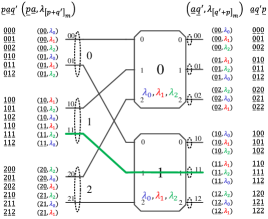
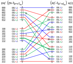
Figure 4: Modular AWG-based shuffle network (a) 𝒲(3,6)𝒲36\mathcal{W}(3,6) and (b) its equivalent shuffle network 𝒩(3,6)𝒩36\mathcal{N}(3,6).
TABLE IV: Connectivity Table 𝑻Dsubscript𝑻𝐷\bm{T}_{D} of 𝒲(3,6)𝒲36\mathcal{W}(3,6)
𝒑\𝒂¯𝒒¯\𝒑¯absent𝒂superscript¯absent𝒒\bm{p}\backslash\underaccent{{\underline{\mskip 7.0mu}}}{\bm{a}}\underaccent{{\underline{\mskip 7.0mu}}}{\bm{q}}^{{}^{\prime}} 𝟎¯𝟎¯¯absent0¯absent0\underaccent{{\underline{\mskip 7.0mu}}}{\bm{0}}\underaccent{{\underline{\mskip 7.0mu}}}{\bm{0}} 𝟎¯𝟏¯¯absent0¯absent1\underaccent{{\underline{\mskip 7.0mu}}}{\bm{0}}\underaccent{{\underline{\mskip 7.0mu}}}{\bm{1}} 𝟎¯𝟐¯¯absent0¯absent2\underaccent{{\underline{\mskip 7.0mu}}}{\bm{0}}\underaccent{{\underline{\mskip 7.0mu}}}{\bm{2}} 𝟏¯𝟎¯¯absent1¯absent0\underaccent{{\underline{\mskip 7.0mu}}}{\bm{1}}\underaccent{{\underline{\mskip 7.0mu}}}{\bm{0}} 𝟏¯𝟏¯¯absent1¯absent1\underaccent{{\underline{\mskip 7.0mu}}}{\bm{1}}\underaccent{{\underline{\mskip 7.0mu}}}{\bm{1}} 𝟏¯𝟐¯¯absent1¯absent2\underaccent{{\underline{\mskip 7.0mu}}}{\bm{1}}\underaccent{{\underline{\mskip 7.0mu}}}{\bm{2}}
00 0¯0¯0¯,0¯0¯0¯¯absent0¯absent0¯absent0¯absent0¯absent0¯absent0\underaccent{{\underline{\mskip 7.0mu}}}{0}\underaccent{{\underline{\mskip 7.0mu}}}{0}\underaccent{{\underline{\mskip 7.0mu}}}{0},\underaccent{{\underline{\mskip 7.0mu}}}{0}\underaccent{{\underline{\mskip 7.0mu}}}{0}\underaccent{{\underline{\mskip 7.0mu}}}{0} 0¯0¯1¯,0¯1¯0¯¯absent0¯absent0¯absent1¯absent0¯absent1¯absent0\underaccent{{\underline{\mskip 7.0mu}}}{0}\underaccent{{\underline{\mskip 7.0mu}}}{0}\underaccent{{\underline{\mskip 7.0mu}}}{1},\underaccent{{\underline{\mskip 7.0mu}}}{0}\underaccent{{\underline{\mskip 7.0mu}}}{1}\underaccent{{\underline{\mskip 7.0mu}}}{0} 0¯0¯2¯,0¯2¯0¯¯absent0¯absent0¯absent2¯absent0¯absent2¯absent0\underaccent{{\underline{\mskip 7.0mu}}}{0}\underaccent{{\underline{\mskip 7.0mu}}}{0}\underaccent{{\underline{\mskip 7.0mu}}}{2},\underaccent{{\underline{\mskip 7.0mu}}}{0}\underaccent{{\underline{\mskip 7.0mu}}}{2}\underaccent{{\underline{\mskip 7.0mu}}}{0} 0¯1¯0¯,1¯0¯0¯¯absent0¯absent1¯absent0¯absent1¯absent0¯absent0\underaccent{{\underline{\mskip 7.0mu}}}{0}\underaccent{{\underline{\mskip 7.0mu}}}{1}\underaccent{{\underline{\mskip 7.0mu}}}{0},\underaccent{{\underline{\mskip 7.0mu}}}{1}\underaccent{{\underline{\mskip 7.0mu}}}{0}\underaccent{{\underline{\mskip 7.0mu}}}{0} 0¯1¯1¯,1¯1¯0¯¯absent0¯absent1¯absent1¯absent1¯absent1¯absent0\underaccent{{\underline{\mskip 7.0mu}}}{0}\underaccent{{\underline{\mskip 7.0mu}}}{1}\underaccent{{\underline{\mskip 7.0mu}}}{1},\underaccent{{\underline{\mskip 7.0mu}}}{1}\underaccent{{\underline{\mskip 7.0mu}}}{1}\underaccent{{\underline{\mskip 7.0mu}}}{0} 0¯1¯2¯,1¯2¯0¯¯absent0¯absent1¯absent2¯absent1¯absent2¯absent0\underaccent{{\underline{\mskip 7.0mu}}}{0}\underaccent{{\underline{\mskip 7.0mu}}}{1}\underaccent{{\underline{\mskip 7.0mu}}}{2},\underaccent{{\underline{\mskip 7.0mu}}}{1}\underaccent{{\underline{\mskip 7.0mu}}}{2}\underaccent{{\underline{\mskip 7.0mu}}}{0}
111 1¯0¯0¯,0¯0¯1¯¯absent1¯absent0¯absent0¯absent0¯absent0¯absent1\underaccent{{\underline{\mskip 7.0mu}}}{1}\underaccent{{\underline{\mskip 7.0mu}}}{0}\underaccent{{\underline{\mskip 7.0mu}}}{0},\underaccent{{\underline{\mskip 7.0mu}}}{0}\underaccent{{\underline{\mskip 7.0mu}}}{0}\underaccent{{\underline{\mskip 7.0mu}}}{1} 1¯0¯1¯,0¯1¯1¯¯absent1¯absent0¯absent1¯absent0¯absent1¯absent1\underaccent{{\underline{\mskip 7.0mu}}}{1}\underaccent{{\underline{\mskip 7.0mu}}}{0}\underaccent{{\underline{\mskip 7.0mu}}}{1},\underaccent{{\underline{\mskip 7.0mu}}}{0}\underaccent{{\underline{\mskip 7.0mu}}}{1}\underaccent{{\underline{\mskip 7.0mu}}}{1} 1¯0¯2¯,0¯2¯1¯¯absent1¯absent0¯absent2¯absent0¯absent2¯absent1\underaccent{{\underline{\mskip 7.0mu}}}{1}\underaccent{{\underline{\mskip 7.0mu}}}{0}\underaccent{{\underline{\mskip 7.0mu}}}{2},\underaccent{{\underline{\mskip 7.0mu}}}{0}\underaccent{{\underline{\mskip 7.0mu}}}{2}\underaccent{{\underline{\mskip 7.0mu}}}{1} 1¯1¯0¯,1¯0¯1¯¯absent1¯absent1¯absent0¯absent1¯absent0¯absent1\underaccent{{\underline{\mskip 7.0mu}}}{1}\underaccent{{\underline{\mskip 7.0mu}}}{1}\underaccent{{\underline{\mskip 7.0mu}}}{0},\underaccent{{\underline{\mskip 7.0mu}}}{1}\underaccent{{\underline{\mskip 7.0mu}}}{0}\underaccent{{\underline{\mskip 7.0mu}}}{1} 1¯1¯1¯,1¯1¯1¯¯absent1¯absent1¯absent1¯absent1¯absent1¯absent1\underaccent{{\underline{\mskip 7.0mu}}}{1}\underaccent{{\underline{\mskip 7.0mu}}}{1}\underaccent{{\underline{\mskip 7.0mu}}}{1},\underaccent{{\underline{\mskip 7.0mu}}}{1}\underaccent{{\underline{\mskip 7.0mu}}}{1}\underaccent{{\underline{\mskip 7.0mu}}}{1} 1¯1¯2¯,1¯2¯1¯¯absent1¯absent1¯absent2¯absent1¯absent2¯absent1\underaccent{{\underline{\mskip 7.0mu}}}{1}\underaccent{{\underline{\mskip 7.0mu}}}{1}\underaccent{{\underline{\mskip 7.0mu}}}{2},\underaccent{{\underline{\mskip 7.0mu}}}{1}\underaccent{{\underline{\mskip 7.0mu}}}{2}\underaccent{{\underline{\mskip 7.0mu}}}{1}
222 2¯0¯0¯,0¯0¯2¯¯absent2¯absent0¯absent0¯absent0¯absent0¯absent2\underaccent{{\underline{\mskip 7.0mu}}}{2}\underaccent{{\underline{\mskip 7.0mu}}}{0}\underaccent{{\underline{\mskip 7.0mu}}}{0},\underaccent{{\underline{\mskip 7.0mu}}}{0}\underaccent{{\underline{\mskip 7.0mu}}}{0}\underaccent{{\underline{\mskip 7.0mu}}}{2} 2¯0¯1¯,0¯1¯2¯¯absent2¯absent0¯absent1¯absent0¯absent1¯absent2\underaccent{{\underline{\mskip 7.0mu}}}{2}\underaccent{{\underline{\mskip 7.0mu}}}{0}\underaccent{{\underline{\mskip 7.0mu}}}{1},\underaccent{{\underline{\mskip 7.0mu}}}{0}\underaccent{{\underline{\mskip 7.0mu}}}{1}\underaccent{{\underline{\mskip 7.0mu}}}{2} 2¯0¯2¯,0¯2¯2¯¯absent2¯absent0¯absent2¯absent0¯absent2¯absent2\underaccent{{\underline{\mskip 7.0mu}}}{2}\underaccent{{\underline{\mskip 7.0mu}}}{0}\underaccent{{\underline{\mskip 7.0mu}}}{2},\underaccent{{\underline{\mskip 7.0mu}}}{0}\underaccent{{\underline{\mskip 7.0mu}}}{2}\underaccent{{\underline{\mskip 7.0mu}}}{2} 2¯1¯0¯,1¯0¯2¯¯absent2¯absent1¯absent0¯absent1¯absent0¯absent2\underaccent{{\underline{\mskip 7.0mu}}}{2}\underaccent{{\underline{\mskip 7.0mu}}}{1}\underaccent{{\underline{\mskip 7.0mu}}}{0},\underaccent{{\underline{\mskip 7.0mu}}}{1}\underaccent{{\underline{\mskip 7.0mu}}}{0}\underaccent{{\underline{\mskip 7.0mu}}}{2} 2¯1¯1¯,1¯1¯2¯¯absent2¯absent1¯absent1¯absent1¯absent1¯absent2\underaccent{{\underline{\mskip 7.0mu}}}{2}\underaccent{{\underline{\mskip 7.0mu}}}{1}\underaccent{{\underline{\mskip 7.0mu}}}{1},\underaccent{{\underline{\mskip 7.0mu}}}{1}\underaccent{{\underline{\mskip 7.0mu}}}{1}\underaccent{{\underline{\mskip 7.0mu}}}{2} 2¯1¯2¯,1¯2¯2¯¯absent2¯absent1¯absent2¯absent1¯absent2¯absent2\underaccent{{\underline{\mskip 7.0mu}}}{2}\underaccent{{\underline{\mskip 7.0mu}}}{1}\underaccent{{\underline{\mskip 7.0mu}}}{2},\underaccent{{\underline{\mskip 7.0mu}}}{1}\underaccent{{\underline{\mskip 7.0mu}}}{2}\underaccent{{\underline{\mskip 7.0mu}}}{2}

According to 𝑻Csubscript𝑻𝐶\bm{T}_{C}, we design the m×rm𝑚𝑟𝑚m\times rm AWG-based shuffle network 𝒲(m,rm)𝒲𝑚𝑟𝑚\mathcal{W}(m,rm) as follows:

  1. S1.

    For each row of 𝑻Csubscript𝑻𝐶\bm{T}_{C}, create an input group, each of which contains r𝑟r inputs, and for each column of 𝑻Csubscript𝑻𝐶\bm{T}_{C}, create an output group, each of which contains one output;

  2. S2.

    Vertically layout r𝑟r m×m𝑚𝑚m\times m AWGs, of which the a𝑎ath m×m𝑚𝑚m\times m AWG is corresponding to the a𝑎ath m×m𝑚𝑚m\times m subtable of 𝑻Csubscript𝑻𝐶\bm{T}_{C}, where a=0,1,,r1𝑎01𝑟1a=0,1,\cdots,r-1;

  3. S3.

    Link the a𝑎ath port of input group p𝑝p, labelled as p¯a¯¯absent𝑝¯absent𝑎\underaccent{{\underline{\mskip 7.0mu}}}{p}\underaccent{{\underline{\mskip 7.0mu}}}{a}, to the p𝑝pth input of the a𝑎ath m×m𝑚𝑚m\times m AWG, for row p𝑝p of 𝑻Csubscript𝑻𝐶\bm{T}_{C} is the p𝑝pth row of the a𝑎ath m×m𝑚𝑚m\times m subtable of 𝑻Csubscript𝑻𝐶\bm{T}_{C}, where p=0,1,,m1𝑝01𝑚1p=0,1,\cdots,m-1;

  4. S4.

    Label output group q𝑞q by a¯q¯¯absent𝑎superscript¯absent𝑞\underaccent{{\underline{\mskip 7.0mu}}}{a}\underaccent{{\underline{\mskip 7.0mu}}}{q}^{\prime} and connect it to the qsuperscript𝑞q^{\prime}th output of the a𝑎ath m×m𝑚𝑚m\times m AWG, if a=q/m𝑎𝑞𝑚a=\lfloor q/m\rfloor and q=[q]msuperscript𝑞subscriptdelimited-[]𝑞𝑚q^{\prime}=[q]_{m}, where q=0,1,,rm1𝑞01𝑟𝑚1q=0,1,\cdots,rm-1.

As Fig. 4 shows, a modular AWG-based shuffle network 𝒲(3,6)𝒲36\mathcal{W}(3,6) is constructed based on 222 3×3333\times 3 AWGs according to Table III.

It’s easy to check that 𝑻Csubscript𝑻𝐶\bm{T}_{C} is the routing table of 𝒲(m,rm)𝒲𝑚𝑟𝑚\mathcal{W}(m,rm). We take the connection between input group p=1𝑝1p=1 and output group a¯q¯=1¯1¯¯absent𝑎superscript¯absent𝑞¯absent1¯absent1\underaccent{{\underline{\mskip 7.0mu}}}{a}\underaccent{{\underline{\mskip 7.0mu}}}{q}^{\prime}=\underaccent{{\underline{\mskip 7.0mu}}}{1}\underaccent{{\underline{\mskip 7.0mu}}}{1} in Fig. 4 as an example. Output group 1¯1¯¯absent1¯absent1\underaccent{{\underline{\mskip 7.0mu}}}{1}\underaccent{{\underline{\mskip 7.0mu}}}{1} is output q=1superscript𝑞1q^{\prime}=1 of AWG a=1𝑎1a=1. In order to visit this output group, the connection from input group p=1𝑝1p=1 must pass through input p=1𝑝1p=1 which is linked to input p=1𝑝1p=1 of AWG a=1𝑎1a=1. In other words, this connection goes through the following path:

input a=1 of input group p=1input 𝑎1 of input group 𝑝1\displaystyle\mbox{input }a=1\mbox{ of input group }p=1
\displaystyle\rightarrow input p=1 of AWG a=1input 𝑝1 of AWG 𝑎1\displaystyle\text{input }p=1\mbox{ of AWG }a=1
\displaystyle\rightarrow input q=1 of AWG a=1.input superscript𝑞1 of AWG 𝑎1\displaystyle\mbox{input }q^{\prime}=1\mbox{ of AWG }a=1.

According to wavelength routing property (1), input p=1𝑝1p=1 of AWG 111 links to output q=1superscript𝑞1q^{\prime}=1 of AWG 111 via wavelength λisubscript𝜆𝑖\lambda_{i}, where

i=[p+q]m=[1+1]3=2.𝑖subscriptdelimited-[]𝑝superscript𝑞𝑚subscriptdelimited-[]1132{i=[p+q^{\prime}]_{m}=[1+1]_{3}=2.} (8)

Accordingly, the wavelength in entry (p,a¯q¯)=(1,1¯1¯)𝑝¯absent𝑎superscript¯absent𝑞1¯absent1¯absent1(p,\underaccent{{\underline{\mskip 7.0mu}}}{a}\underaccent{{\underline{\mskip 7.0mu}}}{q}^{\prime})=(1,\underaccent{{\underline{\mskip 7.0mu}}}{1}\underaccent{{\underline{\mskip 7.0mu}}}{1}) is λ2subscript𝜆2\lambda_{2} in Table III, which verifies that 𝑻Csubscript𝑻𝐶\bm{T}_{C} is the routing table of 𝒲(m,rm)𝒲𝑚𝑟𝑚\mathcal{W}(m,rm).

As this example demonstrates, there is one and only one connection, denoted as C~(p,a¯q¯,λ[p+q]m)~𝐶𝑝¯absent𝑎superscript¯absent𝑞subscript𝜆subscriptdelimited-[]𝑝superscript𝑞𝑚\tilde{C}(p,\underaccent{{\underline{\mskip 7.0mu}}}{a}\underaccent{{\underline{\mskip 7.0mu}}}{q}^{\prime},\lambda_{[p+q^{\prime}]_{m}}), connecting input group p𝑝p and output group a¯q¯¯absent𝑎superscript¯absent𝑞\underaccent{{\underline{\mskip 7.0mu}}}{a}\underaccent{{\underline{\mskip 7.0mu}}}{q}^{\prime}. Once input group p𝑝p and output group a¯q¯¯absent𝑎superscript¯absent𝑞\underaccent{{\underline{\mskip 7.0mu}}}{a}\underaccent{{\underline{\mskip 7.0mu}}}{q}^{\prime} are given, the path and the wavelength λ[p+q]msubscript𝜆subscriptdelimited-[]𝑝superscript𝑞𝑚\lambda_{[p+q^{\prime}]_{m}} of the connection are uniquely determined: p𝑝p and a¯q¯¯absent𝑎superscript¯absent𝑞\underaccent{{\underline{\mskip 7.0mu}}}{a}\underaccent{{\underline{\mskip 7.0mu}}}{q}^{\prime} decide the path while p𝑝p and qsuperscript𝑞q^{\prime} give the wavelength. This indicates that no two connections share the same wavelength at the same port, which means 𝒲(m,rm)𝒲𝑚𝑟𝑚\mathcal{W}(m,rm) has the following property:

Property 2.

𝒲(m,rm)𝒲𝑚𝑟𝑚\mathcal{W}(m,rm) is wavelength contention-free.

Proof:

Consider two connections C~1(p1,a1¯q1¯,λ[p1+q1]m)subscript~𝐶1subscript𝑝1¯absentsubscript𝑎1¯absentsubscriptsuperscript𝑞1subscript𝜆subscriptdelimited-[]subscript𝑝1subscriptsuperscript𝑞1𝑚\tilde{C}_{1}(p_{1},\underaccent{{\underline{\mskip 14.0mu}}}{{a_{1}}}\underaccent{{\underline{\mskip 14.0mu}}}{{q^{\prime}_{1}}},\lambda_{[p_{1}+q^{\prime}_{1}]_{m}}) and C~2(p2,a2¯q2¯,λ[p2+q2]m)subscript~𝐶2subscript𝑝2¯absentsubscript𝑎2¯absentsubscriptsuperscript𝑞2subscript𝜆subscriptdelimited-[]subscript𝑝2subscriptsuperscript𝑞2𝑚\tilde{C}_{2}(p_{2},\underaccent{{\underline{\mskip 14.0mu}}}{{a_{2}}}\underaccent{{\underline{\mskip 14.0mu}}}{{q^{\prime}_{2}}},\lambda_{[p_{2}+q^{\prime}_{2}]_{m}}). Suppose C~1subscript~𝐶1\tilde{C}_{1} and C~2subscript~𝐶2\tilde{C}_{2} originate from the same input and use the same wavelength. Thus, we have

p1=p2=p,subscript𝑝1subscript𝑝2𝑝\displaystyle p_{1}=p_{2}=p,
a1=a2=a,subscript𝑎1subscript𝑎2𝑎\displaystyle a_{1}=a_{2}=a, (9)

and

[p+q1]m=[p+q2]m.subscriptdelimited-[]𝑝subscriptsuperscript𝑞1𝑚subscriptdelimited-[]𝑝subscriptsuperscript𝑞2𝑚{[p+q^{\prime}_{1}]_{m}=[p+q^{\prime}_{2}]_{m}.} (10)

This indicates that q1=q2subscriptsuperscript𝑞1subscriptsuperscript𝑞2{q^{\prime}_{1}=q^{\prime}_{2}} since q1,q2=0,1,,m1formulae-sequencesubscriptsuperscript𝑞1subscriptsuperscript𝑞201𝑚1q^{\prime}_{1},q^{\prime}_{2}=0,1,\cdots,m-1. Hence, C~1subscript~𝐶1\tilde{C}_{1} and C~2subscript~𝐶2\tilde{C}_{2} are the same connection, which means there is no contention at the input side. Following the same argument, we can show there is no connection at the output side. ∎

Property 2 shows that all the connections can be set up without any wavelength contention. It follows that, as long as the input channels and output channels are labelled properly, 𝒲(m,rm)𝒲𝑚𝑟𝑚\mathcal{W}(m,rm) can exhibit the same connection features as 𝒩(m,rm)𝒩𝑚𝑟𝑚\mathcal{N}(m,rm).

According to the structure of 𝑻Csubscript𝑻𝐶\bm{T}_{C}, we assign the address to each wavelength channel of 𝒲(m,rm)𝒲𝑚𝑟𝑚\mathcal{W}(m,rm) as follows:

  1. 1)

    Input channel: Assign addresses to the channels at row p𝑝p (i.e., input group p𝑝p) from left to right. The a¯q¯¯absent𝑎superscript¯absent𝑞\underaccent{{\underline{\mskip 7.0mu}}}{a}\underaccent{{\underline{\mskip 7.0mu}}}{q}^{\prime}th entry at p𝑝pth row is assigned with field address p¯a¯q¯¯absent𝑝¯absent𝑎superscript¯absent𝑞\underaccent{{\underline{\mskip 7.0mu}}}{p}\underaccent{{\underline{\mskip 7.0mu}}}{a}\underaccent{{\underline{\mskip 7.0mu}}}{q}^{\prime} and two-tuple address (p¯a¯,λ[p+q]m)¯absent𝑝¯absent𝑎subscript𝜆subscriptdelimited-[]𝑝superscript𝑞𝑚(\underaccent{{\underline{\mskip 7.0mu}}}{p}\underaccent{{\underline{\mskip 7.0mu}}}{a},\lambda_{[p+q^{\prime}]_{m}}).

  2. 2)

    Output channel: Assign addresses to the channels at column a¯q¯¯absent𝑎superscript¯absent𝑞\underaccent{{\underline{\mskip 7.0mu}}}{a}\underaccent{{\underline{\mskip 7.0mu}}}{q}^{\prime} (i.e., output group a¯q¯¯absent𝑎superscript¯absent𝑞\underaccent{{\underline{\mskip 7.0mu}}}{a}\underaccent{{\underline{\mskip 7.0mu}}}{q}^{\prime}) from top to bottom. The p𝑝pth entry at a¯q¯¯absent𝑎superscript¯absent𝑞\underaccent{{\underline{\mskip 7.0mu}}}{a}\underaccent{{\underline{\mskip 7.0mu}}}{q}^{\prime}th column is assigned with field address a¯q¯p¯¯absent𝑎superscript¯absent𝑞¯absent𝑝\underaccent{{\underline{\mskip 7.0mu}}}{a}\underaccent{{\underline{\mskip 7.0mu}}}{q}^{\prime}\underaccent{{\underline{\mskip 7.0mu}}}{p} and two-tuple address (a¯q¯,λ[q+p]m)¯absent𝑎superscript¯absent𝑞subscript𝜆subscriptdelimited-[]superscript𝑞𝑝𝑚(\underaccent{{\underline{\mskip 7.0mu}}}{a}\underaccent{{\underline{\mskip 7.0mu}}}{q}^{\prime},\lambda_{[q^{\prime}+p]_{m}}).

With this numbering scheme, entry (p,a¯q¯)𝑝¯absent𝑎superscript¯absent𝑞(p,\underaccent{{\underline{\mskip 7.0mu}}}{a}\underaccent{{\underline{\mskip 7.0mu}}}{q}^{\prime}) in 𝑻Csubscript𝑻𝐶\bm{T}_{C} actually indicates that input channel p¯a¯q¯¯absent𝑝¯absent𝑎superscript¯absent𝑞\underaccent{{\underline{\mskip 7.0mu}}}{p}\underaccent{{\underline{\mskip 7.0mu}}}{a}\underaccent{{\underline{\mskip 7.0mu}}}{q}^{\prime} and output channel a¯q¯p¯¯absent𝑎superscript¯absent𝑞¯absent𝑝\underaccent{{\underline{\mskip 7.0mu}}}{a}\underaccent{{\underline{\mskip 7.0mu}}}{q}^{\prime}\underaccent{{\underline{\mskip 7.0mu}}}{p} are connected together via λ[p+q]msubscript𝜆subscriptdelimited-[]𝑝superscript𝑞𝑚\lambda_{[p+q^{\prime}]_{m}}. Similarly, to express such connectivity more explicitly, we replace (p,a¯q¯)𝑝¯absent𝑎superscript¯absent𝑞(p,\underaccent{{\underline{\mskip 7.0mu}}}{a}\underaccent{{\underline{\mskip 7.0mu}}}{q}^{\prime}) with input channel address p¯a¯q¯¯absent𝑝¯absent𝑎superscript¯absent𝑞\underaccent{{\underline{\mskip 7.0mu}}}{p}\underaccent{{\underline{\mskip 7.0mu}}}{a}\underaccent{{\underline{\mskip 7.0mu}}}{q}^{\prime} and output channel address a¯q¯p¯¯absent𝑎superscript¯absent𝑞¯absent𝑝\underaccent{{\underline{\mskip 7.0mu}}}{a}\underaccent{{\underline{\mskip 7.0mu}}}{q}^{\prime}\underaccent{{\underline{\mskip 7.0mu}}}{p}, and obtain a connectivity table of 𝒲(m,rm)𝒲𝑚𝑟𝑚\mathcal{W}(m,rm), called 𝑻Dsubscript𝑻𝐷\bm{T}_{D}. For example, Table IV is the connectivity table of 𝒲(3,6)𝒲36\mathcal{W}(3,6) in Fig. 4.

Table IV clearly shows that modular AWG-based shuffle network 𝒲(m,rm)𝒲𝑚𝑟𝑚\mathcal{W}(m,rm) proposed in this section and network 𝒩(m,rm)𝒩𝑚𝑟𝑚\mathcal{N}(m,rm) have the following equivalence:

Property 3.

AWG-based shuffle network 𝒲(m,rm)𝒲𝑚𝑟𝑚\mathcal{W}(m,rm) is equivalent to a shuffle network 𝒩(m,rm)𝒩𝑚𝑟𝑚\mathcal{N}(m,rm) in terms of the connectivity between input channels and output channels.

Proof:

In 𝒲(m,rm)𝒲𝑚𝑟𝑚\mathcal{W}(m,rm), let’s consider a connection C~(p,a¯q¯,λ[p+q]m)~𝐶𝑝¯absent𝑎superscript¯absent𝑞subscript𝜆subscriptdelimited-[]𝑝superscript𝑞𝑚\tilde{C}(p,\underaccent{{\underline{\mskip 7.0mu}}}{a}\underaccent{{\underline{\mskip 7.0mu}}}{q}^{\prime},\lambda_{[p+q^{\prime}]_{m}}), and assume that q=am+q𝑞𝑎𝑚superscript𝑞q=am+q^{\prime}. As we have shown, there exists a one-one and onto mapping

p,qp,a¯q¯C~(p,a¯q¯,λ[p+q]m).𝑝𝑞𝑝¯absent𝑎superscript¯absent𝑞~𝐶𝑝¯absent𝑎superscript¯absent𝑞subscript𝜆subscriptdelimited-[]𝑝𝑞𝑚{p,q\leftrightarrow p,\underaccent{{\underline{\mskip 7.0mu}}}{a}\underaccent{{\underline{\mskip 7.0mu}}}{q}^{\prime}\leftrightarrow\tilde{C}(p,\underaccent{{\underline{\mskip 7.0mu}}}{a}\underaccent{{\underline{\mskip 7.0mu}}}{q}^{\prime},\lambda_{[p+q]_{m}}).} (11)

According to the connection feature of shuffle network 𝒩(m,rm)𝒩𝑚𝑟𝑚\mathcal{N}(m,rm), the following one-one and onto mapping is set up

p,a¯q¯p,qC(p¯q¯,q¯p¯).𝑝¯absent𝑎superscript¯absent𝑞𝑝𝑞𝐶¯absent𝑝¯absent𝑞¯absent𝑞¯absent𝑝{p,\underaccent{{\underline{\mskip 7.0mu}}}{a}\underaccent{{\underline{\mskip 7.0mu}}}{q}^{\prime}\leftrightarrow p,q\leftrightarrow C(\underaccent{{\underline{\mskip 7.0mu}}}{p}\underaccent{{\underline{\mskip 7.0mu}}}{q},\underaccent{{\underline{\mskip 7.0mu}}}{q}\underaccent{{\underline{\mskip 7.0mu}}}{p}).} (12)

It follows that there is a one-one and onto mapping between connection C~(p,a¯q¯,λ[p+q]m)~𝐶𝑝¯absent𝑎superscript¯absent𝑞subscript𝜆subscriptdelimited-[]𝑝superscript𝑞𝑚\tilde{C}(p,\underaccent{{\underline{\mskip 7.0mu}}}{a}\underaccent{{\underline{\mskip 7.0mu}}}{q}^{\prime},\lambda_{[p+q^{\prime}]_{m}}) in 𝒲(m,rm)𝒲𝑚𝑟𝑚\mathcal{W}(m,rm) and connection C(p¯q¯,q¯p¯)𝐶¯absent𝑝¯absent𝑞¯absent𝑞¯absent𝑝C(\underaccent{{\underline{\mskip 7.0mu}}}{p}\underaccent{{\underline{\mskip 7.0mu}}}{q},\underaccent{{\underline{\mskip 7.0mu}}}{q}\underaccent{{\underline{\mskip 7.0mu}}}{p}) in 𝒩(m,rm)𝒩𝑚𝑟𝑚\mathcal{N}(m,rm), say

C~(p,a¯q¯,λ[p+q]m)C(p¯q¯,q¯p¯).~𝐶𝑝¯absent𝑎superscript¯absent𝑞subscript𝜆subscriptdelimited-[]𝑝superscript𝑞𝑚𝐶¯absent𝑝¯absent𝑞¯absent𝑞¯absent𝑝{\tilde{C}(p,\underaccent{{\underline{\mskip 7.0mu}}}{a}\underaccent{{\underline{\mskip 7.0mu}}}{q}^{\prime},\lambda_{[p+q^{\prime}]_{m}})\leftrightarrow C(\underaccent{{\underline{\mskip 7.0mu}}}{p}\underaccent{{\underline{\mskip 7.0mu}}}{q},\underaccent{{\underline{\mskip 7.0mu}}}{q}\underaccent{{\underline{\mskip 7.0mu}}}{p}).} (13)

Also, according to Property 2, all the connections of 𝒲(m,rm)𝒲𝑚𝑟𝑚\mathcal{W}(m,rm) are achievable without any wavelength contention, which completes the proof. ∎

𝒲(m,rm)𝒲𝑚𝑟𝑚\mathcal{W}(m,rm) exhibits several advantages if it is used to construct an N×N𝑁𝑁N\times N shuffle network, where N=rm2𝑁𝑟superscript𝑚2N=rm^{2}. Firstly, compared to the classical N×N𝑁𝑁N\times N shuffle network, the cabling complexity is small. In particular, the number of fiber links within 𝒲(m,rm)𝒲𝑚𝑟𝑚\mathcal{W}(m,rm) is rm=N/m𝑟𝑚𝑁𝑚rm=N/m, while that of the classical shuffle network is rm2=N𝑟superscript𝑚2𝑁rm^{2}=N. Secondly, the utilization of 𝒲(m,rm)𝒲𝑚𝑟𝑚\mathcal{W}(m,rm) is 100% if all the rm2𝑟superscript𝑚2rm^{2} input wavelength channels are busy, which is similar to the single-AWG based shuffle network. Thirdly, since 𝒲(m,rm)𝒲𝑚𝑟𝑚\mathcal{W}(m,rm) is constructed from r𝑟r m×m𝑚𝑚m\times m AWGs, it possesses good scalability in terms of the following aspects:

  1. 1)

    the wavelength granularity m𝑚m is small;

  2. 2)

    the coherent crosstalk is small,

if the port count of AWGs m𝑚m is small. According to the recent experiment results reported in [37], the power penalty incurred by the coherent crosstalk of 𝒲(m,rm)𝒲𝑚𝑟𝑚\mathcal{W}(m,rm) can be less than 2 dB if we keep m32𝑚32m\leq 32.

IV Awg-based WDM Shuffle-Exchange Network

In this section, our goal is to construct an mn×mnsuperscript𝑚𝑛superscript𝑚𝑛m^{n}\times m^{n} AWG-based WDM SEN. An mn×mnsuperscript𝑚𝑛superscript𝑚𝑛m^{n}\times m^{n} classical SEN is the combination of mn×mnsuperscript𝑚𝑛superscript𝑚𝑛m^{n}\times m^{n} shuffle networks and m×m𝑚𝑚m\times m crossbars, each of which performs switching for an output group of a shuffle network. As Section III shows, the AWG-based shuffle network is a WDM shuffle network, in which each port carries multiple wavelength channels. Also, it is known that the TWC can perform wavelength conversion, and a module consisting of a set of TWCs can perform wavelength switching for the optical signals carried by a fiber link [31]. Therefore, we construct the mn×mnsuperscript𝑚𝑛superscript𝑚𝑛m^{n}\times m^{n} WDM SEN by the combination of the AWG-based shuffle networks and the TWCs in this section.

IV-A mn×mnsuperscript𝑚𝑛superscript𝑚𝑛m^{n}\times m^{n} AWG-based Shuffle Network

The mn×mnsuperscript𝑚𝑛superscript𝑚𝑛m^{n}\times m^{n} shuffle network 𝒲(m,mn1)𝒲𝑚superscript𝑚𝑛1\mathcal{W}(m,m^{n-1}) is a shuffle network 𝒲(m,rm)𝒲𝑚𝑟𝑚\mathcal{W}(m,rm) with r=mn2𝑟superscript𝑚𝑛2r=m^{n-2}. Since there are m𝑚m input groups, mn2superscript𝑚𝑛2m^{n-2} inputs in each group, and m𝑚m wavelength channels at each input in 𝒲(m,mn1)𝒲𝑚superscript𝑚𝑛1\mathcal{W}(m,m^{n-1}), for an input wavelength channel X=p¯a¯q¯𝑋¯absent𝑝¯absent𝑎superscript¯absent𝑞X=\underaccent{{\underline{\mskip 7.0mu}}}{p}\underaccent{{\underline{\mskip 7.0mu}}}{a}\underaccent{{\underline{\mskip 7.0mu}}}{q}^{\prime}, the address X𝑋X can be relabeled by an m𝑚m-ary n𝑛n-field address xn¯xn1¯x2¯x1¯¯absentsubscript𝑥𝑛¯absentsubscript𝑥𝑛1¯absentsubscript𝑥2¯absentsubscript𝑥1\underaccent{{\underline{\mskip 19.0mu}}}{{x_{n}}}\underaccent{{\underline{\mskip 45.0mu}}}{{x_{n-1}}}\cdots\underaccent{{\underline{\mskip 19.0mu}}}{{x_{2}}}\underaccent{{\underline{\mskip 19.0mu}}}{{x_{1}}} where xnsubscript𝑥𝑛x_{n} is corresponding to group address p𝑝p, xn1¯x2¯¯absentsubscript𝑥𝑛1¯absentsubscript𝑥2\underaccent{{\underline{\mskip 45.0mu}}}{{x_{n-1}}}\cdots\underaccent{{\underline{\mskip 19.0mu}}}{{x_{2}}} corresponding to port address a𝑎a, and x1subscript𝑥1x_{1} corresponding to wavelength address qsuperscript𝑞q^{\prime}. Accordingly, two-tuple address X~=(p¯a¯,λ[p+q]m)~𝑋¯absent𝑝¯absent𝑎subscript𝜆subscriptdelimited-[]𝑝superscript𝑞𝑚\tilde{X}=(\underaccent{{\underline{\mskip 7.0mu}}}{p}\underaccent{{\underline{\mskip 7.0mu}}}{a},\lambda_{[p+q^{\prime}]_{m}}) can be represented as (xn¯xn1¯x2¯,λ[xn+x1]m)¯absentsubscript𝑥𝑛¯absentsubscript𝑥𝑛1¯absentsubscript𝑥2subscript𝜆subscriptdelimited-[]subscript𝑥𝑛subscript𝑥1𝑚(\underaccent{{\underline{\mskip 19.0mu}}}{{x_{n}}}\underaccent{{\underline{\mskip 45.0mu}}}{{x_{n-1}}}\cdots\underaccent{{\underline{\mskip 19.0mu}}}{{x_{2}}},\lambda_{[x_{n}+x_{1}]_{m}}). At the output side, there are mn1superscript𝑚𝑛1m^{n-1} output groups (or outputs), and m𝑚m wavelength channels at each input. Thus, an output wavelength channel Y=a¯q¯p¯𝑌¯absent𝑎superscript¯absent𝑞¯absent𝑝Y=\underaccent{{\underline{\mskip 7.0mu}}}{a}\underaccent{{\underline{\mskip 7.0mu}}}{q}^{\prime}\underaccent{{\underline{\mskip 7.0mu}}}{p} can also be represented as yn¯yn1¯y2¯y1¯¯absentsubscript𝑦𝑛¯absentsubscript𝑦𝑛1¯absentsubscript𝑦2¯absentsubscript𝑦1\underaccent{{\underline{\mskip 19.0mu}}}{{y_{n}}}\underaccent{{\underline{\mskip 45.0mu}}}{{y_{n-1}}}\cdots\underaccent{{\underline{\mskip 19.0mu}}}{{y_{2}}}\underaccent{{\underline{\mskip 19.0mu}}}{{y_{1}}}, where yn¯yn1¯y2¯¯absentsubscript𝑦𝑛¯absentsubscript𝑦𝑛1¯absentsubscript𝑦2\underaccent{{\underline{\mskip 19.0mu}}}{{y_{n}}}\underaccent{{\underline{\mskip 45.0mu}}}{{y_{n-1}}}\cdots\underaccent{{\underline{\mskip 19.0mu}}}{{y_{2}}} is corresponding to group address a¯q¯¯absent𝑎superscript¯absent𝑞\underaccent{{\underline{\mskip 7.0mu}}}{a}\underaccent{{\underline{\mskip 7.0mu}}}{q}^{\prime}, and y1subscript𝑦1y_{1} corresponding to p𝑝p. Correspondingly, two-tuple address Y~=(a¯q¯,λ[q+p]m)~𝑌¯absent𝑎superscript¯absent𝑞subscript𝜆subscriptdelimited-[]superscript𝑞𝑝𝑚\tilde{Y}=(\underaccent{{\underline{\mskip 7.0mu}}}{a}\underaccent{{\underline{\mskip 7.0mu}}}{q}^{\prime},\lambda_{[q^{\prime}+p]_{m}}) can be rewritten as (yn¯yn1¯y2¯,λ[y2+y1]m)¯absentsubscript𝑦𝑛¯absentsubscript𝑦𝑛1¯absentsubscript𝑦2subscript𝜆subscriptdelimited-[]subscript𝑦2subscript𝑦1𝑚(\underaccent{{\underline{\mskip 19.0mu}}}{{y_{n}}}\underaccent{{\underline{\mskip 45.0mu}}}{{y_{n-1}}}\cdots\underaccent{{\underline{\mskip 19.0mu}}}{{y_{2}}},\lambda_{[y_{2}+y_{1}]_{m}}). According to the discussions in Section III, 𝒲(m,mn1)𝒲𝑚superscript𝑚𝑛1\mathcal{W}(m,m^{n-1}) has the following connection property:

Refer to caption
Refer to caption
Figure 5: Illustration of TWC-modules: (a) a 3×3333\times 3 TWC-module and (b) its space representation.
Refer to caption
Refer to caption
Figure 6: Illustration of AWG-based WDM SENs: (a) An AWG-based WDM SEN 𝒮(m,n)𝒮𝑚𝑛\mathcal{S}(m,n) and (b) its space representation.
X=𝑋absent\displaystyle X= p¯a¯q¯=xn¯xn1¯x2¯x1¯¯absent𝑝¯absent𝑎superscript¯absent𝑞¯absentsubscript𝑥𝑛¯absentsubscript𝑥𝑛1¯absentsubscript𝑥2¯absentsubscript𝑥1\displaystyle\underaccent{{\underline{\mskip 7.0mu}}}{p}\underaccent{{\underline{\mskip 7.0mu}}}{a}\underaccent{{\underline{\mskip 7.0mu}}}{q}^{\prime}=\underaccent{{\underline{\mskip 19.0mu}}}{{x_{n}}}\underaccent{{\underline{\mskip 45.0mu}}}{{x_{n-1}}}\cdots\underaccent{{\underline{\mskip 19.0mu}}}{{x_{2}}}\underaccent{{\underline{\mskip 19.0mu}}}{{x_{1}}}
Y=absent𝑌absent\displaystyle\rightarrow Y= a¯q¯p¯=xn1¯x2¯x1¯xn¯¯absent𝑎superscript¯absent𝑞¯absent𝑝¯absentsubscript𝑥𝑛1¯absentsubscript𝑥2¯absentsubscript𝑥1¯absentsubscript𝑥𝑛\displaystyle\underaccent{{\underline{\mskip 7.0mu}}}{a}\underaccent{{\underline{\mskip 7.0mu}}}{q}^{\prime}\underaccent{{\underline{\mskip 7.0mu}}}{p}=\underaccent{{\underline{\mskip 45.0mu}}}{{x_{n-1}}}\cdots\underaccent{{\underline{\mskip 19.0mu}}}{{x_{2}}}\underaccent{{\underline{\mskip 19.0mu}}}{{x_{1}}}\underaccent{{\underline{\mskip 19.0mu}}}{{x_{n}}} (14)

or

X~=~𝑋absent\displaystyle\tilde{X}= (p¯a¯,λ[p+q]m)=(xn¯xn1¯x2¯,λ[xn+x1]m)¯absent𝑝¯absent𝑎subscript𝜆subscriptdelimited-[]𝑝superscript𝑞𝑚¯absentsubscript𝑥𝑛¯absentsubscript𝑥𝑛1¯absentsubscript𝑥2subscript𝜆subscriptdelimited-[]subscript𝑥𝑛subscript𝑥1𝑚\displaystyle(\underaccent{{\underline{\mskip 7.0mu}}}{p}\underaccent{{\underline{\mskip 7.0mu}}}{a},\lambda_{[p+q^{\prime}]_{m}})=(\underaccent{{\underline{\mskip 19.0mu}}}{{x_{n}}}\underaccent{{\underline{\mskip 45.0mu}}}{{x_{n-1}}}\cdots\underaccent{{\underline{\mskip 19.0mu}}}{{x_{2}}},\lambda_{[x_{n}+x_{1}]_{m}})
Y~=absent~𝑌absent\displaystyle\rightarrow\tilde{Y}= (a¯q¯,λ[p+q]m)=(xn1¯x2¯x1¯,λ[xn+x1]m).¯absent𝑎superscript¯absent𝑞subscript𝜆subscriptdelimited-[]𝑝superscript𝑞𝑚¯absentsubscript𝑥𝑛1¯absentsubscript𝑥2¯absentsubscript𝑥1subscript𝜆subscriptdelimited-[]subscript𝑥𝑛subscript𝑥1𝑚\displaystyle(\underaccent{{\underline{\mskip 7.0mu}}}{a}\underaccent{{\underline{\mskip 7.0mu}}}{q}^{\prime},\lambda_{[p+q^{\prime}]_{m}})=(\underaccent{{\underline{\mskip 45.0mu}}}{{x_{n-1}}}\cdots\underaccent{{\underline{\mskip 19.0mu}}}{{x_{2}}}\underaccent{{\underline{\mskip 19.0mu}}}{{x_{1}}},\lambda_{[x_{n}+x_{1}]_{m}}). (15)

IV-B TWC-module

An m×m𝑚𝑚m\times m TWC-module consists of m𝑚m TWCs sandwiched by a 1×m1𝑚1\times m DeMux, and an m×1𝑚1m\times 1 Mux, as Fig. 5(a) illustrates. The function of the TWC-module is to convert a wavelength set Δ={δ0,δ1,,δm1}Δsubscript𝛿0subscript𝛿1subscript𝛿𝑚1\Delta=\{\delta_{0},\delta_{1},\cdots,\delta_{m-1}\} at the input fiber to a wavelength set Ω={ω0,ω1,,ωm1}Ωsubscript𝜔0subscript𝜔1subscript𝜔𝑚1\Omega=\{\omega_{0},\omega_{1},\cdots,\omega_{m-1}\} at the output fiber. In other words, the TWC-module performs a wavelength conversion mapping ϕ:ΔΩ:italic-ϕΔΩ\phi:\Delta\rightarrow\Omega. Thus, if we consider each input wavelength as an input and each output wavelength as an output, an m×m𝑚𝑚m\times m TWC-module is logically equivalent to an m×m𝑚𝑚m\times m crossbar. As an example, Fig. 5 plots a 3×3333\times 3 TWC-module and its space representation, which demonstrates the equivalence between the 3×3333\times 3 TWC-module and the 3×3333\times 3 crossbar.

The size m𝑚m of the set ΩΩ\Omega is referred to as conversion range, which actually characterizes the capability of the TWC-module. The conversion range is larger, the synthesis difficulty and thus the cost of the TWC-module are larger. Therefore, the conversion range of the TWC-modules employed in optical switching systems should not be very large.

To facilitate the discussion, we assume that there is a fictitious wavelength boundary in the middle of the TWC-module, and the wavelength conversions happen at this boundary [31], as the dashed line in Fig. 5 illustrates. Such wavelength boundary logically divides the TWC-module into left part and right part, called L-TWC-module and R-TWC-module respectively, and the wavelength sets used in these two parts are mutually independent.

IV-C AWG-based WDM SEN
Refer to caption
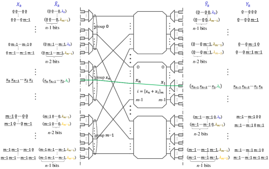
Figure 7: The k𝑘kth shuffle stage 𝒲ksubscript𝒲𝑘\mathcal{W}_{k}.

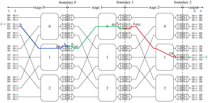
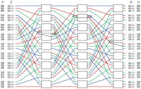
An mn×mnsuperscript𝑚𝑛superscript𝑚𝑛m^{n}\times m^{n} AWG-based WDM SEN proposed in this paper is constructed from n𝑛n cascaded mn×mnsuperscript𝑚𝑛superscript𝑚𝑛m^{n}\times m^{n} AWG-based WDM shuffle networks, in each of which every output is attached by an m×m𝑚𝑚m\times m TWC-module. We denote such AWG-based WDM SEN by 𝒮(m,n)𝒮𝑚𝑛\mathcal{S}(m,n). It is clear that there are n𝑛n columns of m×m𝑚𝑚m\times m TWC-modules in 𝒮(m,n)𝒮𝑚𝑛\mathcal{S}(m,n), and each column contains mn1superscript𝑚𝑛1m^{n-1} TWC-modules. An example is the 33×33superscript33superscript333^{3}\times 3^{3} AWG-based WDM SEN 𝒮(3,3)𝒮33\mathcal{S}(3,3) in Fig. 6. This network is functionally equivalent with the mn×mnsuperscript𝑚𝑛superscript𝑚𝑛m^{n}\times m^{n} classical SEN, which can be demonstrated by the following correspondences:

  1. 1)

    Each mn×mnsuperscript𝑚𝑛superscript𝑚𝑛m^{n}\times m^{n} AWG-based shuffle network 𝒲(m,mn1)𝒲𝑚superscript𝑚𝑛1\mathcal{W}(m,m^{n-1}) is corresponding to a shuffle network 𝒩(m,mn1)𝒩𝑚superscript𝑚𝑛1\mathcal{N}(m,m^{n-1});

  2. 2)

    Each m×m𝑚𝑚m\times m TWC-module is corresponding to an m×m𝑚𝑚m\times m crossbar.

For example, after the correspondences, the 33×33superscript33superscript333^{3}\times 3^{3} AWG-based WDM SEN in Fig. 6 changes to the 33×33superscript33superscript333^{3}\times 3^{3} switching network in Fig. 6, which is clearly a SEN.

S~=(0¯1¯,λ0)S=0¯1¯0¯𝒲0(1¯0¯,λ0)1¯0¯0¯boundary 0(1¯0¯,λ2)1¯0¯1¯𝒲1(0¯1¯,λ2)0¯1¯1¯boundary 1(0¯1¯,λ1)0¯1¯1¯𝒲2(1¯1¯,λ1)1¯1¯0¯boundary 2(1¯1¯,λ2)=D~1¯1¯1¯=Dsubscript𝒲0~𝑆¯absent0¯absent1subscript𝜆0𝑆¯absent0¯absent1¯absent0¯absent1¯absent0subscript𝜆0¯absent1¯absent0¯absent0boundary 0¯absent1¯absent0subscript𝜆2¯absent1¯absent0¯absent1subscript𝒲1¯absent0¯absent1subscript𝜆2¯absent0¯absent1¯absent1boundary 1¯absent0¯absent1subscript𝜆1¯absent0¯absent1¯absent1subscript𝒲2¯absent1¯absent1subscript𝜆1¯absent1¯absent1¯absent0boundary 2¯absent1¯absent1subscript𝜆2~𝐷¯absent1¯absent1¯absent1𝐷{\begin{split}\tilde{S}=(\underaccent{{\underline{\mskip 7.0mu}}}{0}\underaccent{{\underline{\mskip 7.0mu}}}{1}&,\lambda_{0})\\ S=\underaccent{{\underline{\mskip 7.0mu}}}{0}&\underaccent{{\underline{\mskip 7.0mu}}}{1}\underaccent{{\underline{\mskip 7.0mu}}}{0}\end{split}}\xrightarrow[]{\mathcal{W}_{0}}{\begin{split}(\underaccent{{\underline{\mskip 7.0mu}}}{1}\underaccent{{\underline{\mskip 7.0mu}}}{0}&,\lambda_{0})\\ \underaccent{{\underline{\mskip 7.0mu}}}{1}&\underaccent{{\underline{\mskip 7.0mu}}}{0}\underaccent{{\underline{\mskip 7.0mu}}}{0}\end{split}}\xrightarrow[]{\mbox{boundary\ 0}}{\begin{split}(\underaccent{{\underline{\mskip 7.0mu}}}{1}\underaccent{{\underline{\mskip 7.0mu}}}{0}&,\lambda_{2})\\ \underaccent{{\underline{\mskip 7.0mu}}}{1}&\underaccent{{\underline{\mskip 7.0mu}}}{0}\underaccent{{\underline{\mskip 7.0mu}}}{1}\end{split}}\xrightarrow[]{\mathcal{W}_{1}}{\begin{split}(\underaccent{{\underline{\mskip 7.0mu}}}{0}\underaccent{{\underline{\mskip 7.0mu}}}{1}&,\lambda_{2})\\ \underaccent{{\underline{\mskip 7.0mu}}}{0}&\underaccent{{\underline{\mskip 7.0mu}}}{1}\underaccent{{\underline{\mskip 7.0mu}}}{1}\end{split}}\xrightarrow[]{\mbox{boundary\ 1}}{\begin{split}(\underaccent{{\underline{\mskip 7.0mu}}}{0}\underaccent{{\underline{\mskip 7.0mu}}}{1}&,\lambda_{1})\\ \underaccent{{\underline{\mskip 7.0mu}}}{0}&\underaccent{{\underline{\mskip 7.0mu}}}{1}\underaccent{{\underline{\mskip 7.0mu}}}{1}\end{split}}\xrightarrow[]{\mathcal{W}_{2}}{\begin{split}(\underaccent{{\underline{\mskip 7.0mu}}}{1}\underaccent{{\underline{\mskip 7.0mu}}}{1}&,\lambda_{1})\\ \underaccent{{\underline{\mskip 7.0mu}}}{1}&\underaccent{{\underline{\mskip 7.0mu}}}{1}\underaccent{{\underline{\mskip 7.0mu}}}{0}\end{split}}\xrightarrow[]{\mbox{boundary\ 2}}{\begin{split}(\underaccent{{\underline{\mskip 7.0mu}}}{1}\underaccent{{\underline{\mskip 7.0mu}}}{1},&\lambda_{2})=\tilde{D}\\ \underaccent{{\underline{\mskip 7.0mu}}}{1}\underaccent{{\underline{\mskip 7.0mu}}}{1}&\underaccent{{\underline{\mskip 7.0mu}}}{1}=D\end{split}} (16)

As the dotted lines in Fig. 6 illustrates, the middle of each column of TWC-modules in 𝒮(m,n)𝒮𝑚𝑛\mathcal{S}(m,n) forms a virtual wavelength boundary, at which the wavelength exchanges are performed. Thus, these n𝑛n boundaries divide network 𝒮(m,n)𝒮𝑚𝑛\mathcal{S}(m,n) into n+1𝑛1n+1 regions, and the wavelength sets in different regions are mutually independent. We refer to the first n𝑛n regions as shuffle stages, and the last region output stage. Each shuffle stage is a 𝒲(m,mn1)𝒲𝑚superscript𝑚𝑛1\mathcal{W}(m,m^{n-1}) sandwiched by a column of R-TWC modules and a column of L-TWC modules, as Fig. 7 demonstrates. Note that the L-TWC module (R-TWC module) actually only performs wavelength multiplexing (demulitplexing) instead of wavelength conversion. Thus, each shuffle stage is actually a shuffle network 𝒲(m,mn1)𝒲𝑚superscript𝑚𝑛1\mathcal{W}(m,m^{n-1}). We thus denote the k𝑘kth shuffle stage as 𝒲ksubscript𝒲𝑘\mathcal{W}_{k}. Let Xksubscript𝑋𝑘X_{k} and Yksubscript𝑌𝑘Y_{k} be the field addresses of the input wavelength channel and the output wavelength channel, and X~ksubscript~𝑋𝑘\tilde{X}_{k} and Y~ksubscript~𝑌𝑘\tilde{Y}_{k} be the two-tuple address. The connection property of 𝒲ksubscript𝒲𝑘\mathcal{W}_{k} is delineated by (14) and (15). As Fig. 7 plots, input wavelength channel

Xk=xn¯xn1¯x2¯x1¯subscript𝑋𝑘¯absentsubscript𝑥𝑛¯absentsubscript𝑥𝑛1¯absentsubscript𝑥2¯absentsubscript𝑥1X_{k}=\underaccent{{\underline{\mskip 19.0mu}}}{{x_{n}}}\underaccent{{\underline{\mskip 45.0mu}}}{{x_{n-1}}}\cdots\underaccent{{\underline{\mskip 19.0mu}}}{{x_{2}}}\underaccent{{\underline{\mskip 19.0mu}}}{{x_{1}}}

or

X~k=(xn¯xn1¯x2¯,λi)subscript~𝑋𝑘¯absentsubscript𝑥𝑛¯absentsubscript𝑥𝑛1¯absentsubscript𝑥2subscript𝜆𝑖\tilde{X}_{k}=(\underaccent{{\underline{\mskip 19.0mu}}}{{x_{n}}}\underaccent{{\underline{\mskip 45.0mu}}}{{x_{n-1}}}\cdots\underaccent{{\underline{\mskip 19.0mu}}}{{x_{2}}},\lambda_{i})

is connected to output wavelength channel

Yk=xn1¯x2¯x1¯xn¯subscript𝑌𝑘¯absentsubscript𝑥𝑛1¯absentsubscript𝑥2¯absentsubscript𝑥1¯absentsubscript𝑥𝑛Y_{k}=\underaccent{{\underline{\mskip 45.0mu}}}{{x_{n-1}}}\cdots\underaccent{{\underline{\mskip 19.0mu}}}{{x_{2}}}\underaccent{{\underline{\mskip 19.0mu}}}{{x_{1}}}\underaccent{{\underline{\mskip 19.0mu}}}{{x_{n}}}

or

X~k=(xn1¯x2¯x1¯,λi),subscript~𝑋𝑘¯absentsubscript𝑥𝑛1¯absentsubscript𝑥2¯absentsubscript𝑥1subscript𝜆𝑖\tilde{X}_{k}=(\underaccent{{\underline{\mskip 45.0mu}}}{{x_{n-1}}}\cdots\underaccent{{\underline{\mskip 19.0mu}}}{{x_{2}}}\underaccent{{\underline{\mskip 19.0mu}}}{{x_{1}}},\lambda_{i}),

where

i=[xn+x1]m.𝑖subscriptdelimited-[]subscript𝑥𝑛subscript𝑥1𝑚i=[x_{n}+x_{1}]_{m}.

Due to the regular topology, we assign the addresses to the input channels and the output channels of 𝒮(m,n)𝒮𝑚𝑛\mathcal{S}(m,n) as follows. Firstly, the input channels of 𝒮(m,n)𝒮𝑚𝑛\mathcal{S}(m,n) are the input channels of 𝒲0subscript𝒲0\mathcal{W}_{0}. Therefore, the address of the input channels of 𝒮(m,n)𝒮𝑚𝑛\mathcal{S}(m,n) can be the same with that of the input channel of 𝒲0subscript𝒲0\mathcal{W}_{0}. That is, wavelength channel λisubscript𝜆𝑖\lambda_{i} at the a𝑎ath input of the p𝑝pth input group is assigned with a two-tuple address S~=(sn¯sn1¯s2¯,λi)~𝑆¯absentsubscript𝑠𝑛¯absentsubscript𝑠𝑛1¯absentsubscript𝑠2subscript𝜆𝑖\tilde{S}=(\underaccent{{\underline{\mskip 19.0mu}}}{{s_{n}}}\underaccent{{\underline{\mskip 45.0mu}}}{{s_{n-1}}}\cdots\underaccent{{\underline{\mskip 19.0mu}}}{{s_{2}}},\lambda_{i}) and a field address S=sn¯sn1¯s2¯s1¯𝑆¯absentsubscript𝑠𝑛¯absentsubscript𝑠𝑛1¯absentsubscript𝑠2¯absentsubscript𝑠1S=\underaccent{{\underline{\mskip 19.0mu}}}{{s_{n}}}\underaccent{{\underline{\mskip 45.0mu}}}{{s_{n-1}}}\cdots\underaccent{{\underline{\mskip 19.0mu}}}{{s_{2}}}\underaccent{{\underline{\mskip 19.0mu}}}{{s_{1}}}, where sn=psubscript𝑠𝑛𝑝s_{n}=p, sn1¯s2¯¯absentsubscript𝑠𝑛1¯absentsubscript𝑠2\underaccent{{\underline{\mskip 45.0mu}}}{{s_{n-1}}}\cdots\underaccent{{\underline{\mskip 19.0mu}}}{{s_{2}}} is the m𝑚m-ary number of a𝑎a, and s1=[isn]msubscript𝑠1subscriptdelimited-[]𝑖subscript𝑠𝑛𝑚s_{1}=[i-s_{n}]_{m}. The output stage is a column of R-TWC-modules, and can be regarded as the input of a truncated shuffle stage, of which the shuffle network and the column of L-TWC-modules are removed. Thus, we label the output channels in the same way. Different from the input channel address, we use D~=(dn¯dn1¯d2¯,λi)~𝐷¯absentsubscript𝑑𝑛¯absentsubscript𝑑𝑛1¯absentsubscript𝑑2subscript𝜆𝑖\tilde{D}=(\underaccent{{\underline{\mskip 19.0mu}}}{{d_{n}}}\underaccent{{\underline{\mskip 45.0mu}}}{{d_{n-1}}}\cdots\underaccent{{\underline{\mskip 19.0mu}}}{{d_{2}}},\lambda_{i}) or D=dn¯dn1¯d2¯d1¯𝐷¯absentsubscript𝑑𝑛¯absentsubscript𝑑𝑛1¯absentsubscript𝑑2¯absentsubscript𝑑1D=\underaccent{{\underline{\mskip 19.0mu}}}{{d_{n}}}\underaccent{{\underline{\mskip 45.0mu}}}{{d_{n-1}}}\cdots\underaccent{{\underline{\mskip 19.0mu}}}{{d_{2}}}\underaccent{{\underline{\mskip 19.0mu}}}{{d_{1}}} to denote wavelength channel λisubscript𝜆𝑖\lambda_{i} at the a𝑎ath output of the p𝑝pth output group.

It is clear that mn×mnsuperscript𝑚𝑛superscript𝑚𝑛m^{n}\times m^{n} AWG-based SEN 𝒮(m,n)𝒮𝑚𝑛\mathcal{S}(m,n) has good scalability, since it is constructed from a set of m×m𝑚𝑚m\times m AWGs and TWCs with a conversion range of m𝑚m. Again, if we keep m32𝑚32m\leq 32, the coherent crosstalk at each stage can be smaller than 2 dB such that it can be compensated at the outputs of each m×m𝑚𝑚m\times m AWGs.

This architecture has another important scalability advantage. The most common implementation of TWC is by an opto-electronic transponder that converts optical signals into electronic form and reconverts back into the optical domain onto another wavelength. In doing this operation, the TWC also performs full digital regeneration (3R) of the signals. It should be noted that each shuffle stage is connected to the next by an array of TWCs. Thus, this implies that all the signals are 3R-regenerated from stage to stage. Therefore, signal impairments, such as coherent crosstalk, do not accumulate from stage to stage, making the network highly scalable in terms of number of cascaded stages.

TABLE V: Routing Path of R(S~,D~)𝑅~𝑆~𝐷R(\tilde{S},\tilde{D}) in AWG-Based SEN
shuffle routing path wavelength assignment
stage 0 S~=X~0=(sn¯sn1¯s2¯,λi0\tilde{S}=\tilde{X}_{0}=(\underaccent{{\underline{\mskip 19.0mu}}}{{s_{n}}}\underaccent{{\underline{\mskip 45.0mu}}}{{s_{n-1}}}\cdots\underaccent{{\underline{\mskip 19.0mu}}}{{s_{2}}},\lambda_{i_{0}}) \rightarrow Y~0=(sn1¯sn2¯s1¯,λi0)subscript~𝑌0¯absentsubscript𝑠𝑛1¯absentsubscript𝑠𝑛2¯absentsubscript𝑠1subscript𝜆subscript𝑖0\tilde{Y}_{0}=(\underaccent{{\underline{\mskip 45.0mu}}}{{s_{n-1}}}\underaccent{{\underline{\mskip 45.0mu}}}{{s_{n-2}}}\cdots\underaccent{{\underline{\mskip 19.0mu}}}{{s_{1}}},\lambda_{i_{0}}) i0=[sn+s1]msubscript𝑖0subscriptdelimited-[]subscript𝑠𝑛subscript𝑠1𝑚i_{0}=[s_{n}+s_{1}]_{m}
S=X0=sn¯sn1¯s2¯s1¯𝑆subscript𝑋0¯absentsubscript𝑠𝑛¯absentsubscript𝑠𝑛1¯absentsubscript𝑠2¯absentsubscript𝑠1S=X_{0}=\underaccent{{\underline{\mskip 19.0mu}}}{{s_{n}}}\underaccent{{\underline{\mskip 45.0mu}}}{{s_{n-1}}}\cdots\underaccent{{\underline{\mskip 19.0mu}}}{{s_{2}}}\underaccent{{\underline{\mskip 19.0mu}}}{{s_{1}}} Y0=sn1¯sn2¯s1¯sn¯subscript𝑌0¯absentsubscript𝑠𝑛1¯absentsubscript𝑠𝑛2¯absentsubscript𝑠1¯absentsubscript𝑠𝑛Y_{0}=\underaccent{{\underline{\mskip 45.0mu}}}{{s_{n-1}}}\underaccent{{\underline{\mskip 45.0mu}}}{{s_{n-2}}}\cdots\underaccent{{\underline{\mskip 19.0mu}}}{{s_{1}}}\underaccent{{\underline{\mskip 19.0mu}}}{{s_{n}}}
\cdots
stage k𝑘k \rightarrow X~k=(snk¯dnk+2¯,λik)subscript~𝑋𝑘¯absentsubscript𝑠𝑛𝑘¯absentsubscript𝑑𝑛𝑘2subscript𝜆subscript𝑖𝑘\tilde{X}_{k}=(\underaccent{{\underline{\mskip 45.0mu}}}{{s_{n-k}}}\cdots\underaccent{{\underline{\mskip 71.0mu}}}{{d_{n-k+2}}},\lambda_{i_{k}}) \rightarrow Y~k=(snk1¯dnk+1¯,λik)subscript~𝑌𝑘¯absentsubscript𝑠𝑛𝑘1¯absentsubscript𝑑𝑛𝑘1subscript𝜆subscript𝑖𝑘\tilde{Y}_{k}=(\underaccent{{\underline{\mskip 66.0mu}}}{{s_{n-k-1}}}\cdots\underaccent{{\underline{\mskip 66.0mu}}}{{d_{n-k+1}}},\lambda_{i_{k}}) ik=[snk+dnk+1]msubscript𝑖𝑘subscriptdelimited-[]subscript𝑠𝑛𝑘subscript𝑑𝑛𝑘1𝑚i_{k}=[s_{n-k}+d_{n-k+1}]_{m}
Xk=snk¯dnk+2¯dnk+1¯subscript𝑋𝑘¯absentsubscript𝑠𝑛𝑘¯absentsubscript𝑑𝑛𝑘2¯absentsubscript𝑑𝑛𝑘1X_{k}=\underaccent{{\underline{\mskip 45.0mu}}}{{s_{n-k}}}\cdots\underaccent{{\underline{\mskip 66.0mu}}}{{d_{n-k+2}}}\underaccent{{\underline{\mskip 66.0mu}}}{{d_{n-k+1}}} Yk=snk1¯dnk+1¯snk¯subscript𝑌𝑘¯absentsubscript𝑠𝑛𝑘1¯absentsubscript𝑑𝑛𝑘1¯absentsubscript𝑠𝑛𝑘Y_{k}=\underaccent{{\underline{\mskip 66.0mu}}}{{s_{n-k-1}}}\cdots\underaccent{{\underline{\mskip 66.0mu}}}{{d_{n-k+1}}}\underaccent{{\underline{\mskip 45.0mu}}}{{s_{n-k}}}
\cdots
output stage
\rightarrow (dn¯dn1¯d2¯,λin)=D~¯absentsubscript𝑑𝑛¯absentsubscript𝑑𝑛1¯absentsubscript𝑑2subscript𝜆subscript𝑖𝑛~𝐷(\underaccent{{\underline{\mskip 19.0mu}}}{{d_{n}}}\underaccent{{\underline{\mskip 45.0mu}}}{{d_{n-1}}}\cdots\underaccent{{\underline{\mskip 19.0mu}}}{{d_{2}}},\lambda_{i_{n}})=\tilde{D}
    dn¯dn1¯d2¯d1¯=D¯absentsubscript𝑑𝑛¯absentsubscript𝑑𝑛1¯absentsubscript𝑑2¯absentsubscript𝑑1𝐷\underaccent{{\underline{\mskip 19.0mu}}}{{d_{n}}}\underaccent{{\underline{\mskip 45.0mu}}}{{d_{n-1}}}\cdots\underaccent{{\underline{\mskip 19.0mu}}}{{d_{2}}}\underaccent{{\underline{\mskip 19.0mu}}}{{d_{1}}}=D
in=[dn+d1]msubscript𝑖𝑛subscriptdelimited-[]subscript𝑑𝑛subscript𝑑1𝑚i_{n}=[d_{n}+d_{1}]_{m}

V RWA in AWG-based WDM SENs

One of the most interesting properties of the classical SEN is the self-routing property. Consider a classical mn×mnsuperscript𝑚𝑛superscript𝑚𝑛m^{n}\times m^{n} SEN, where each input port or each output port is assigned with an m𝑚m-ary n𝑛n-field address. Once input address S=sn¯sn1¯s2¯s1¯𝑆¯absentsubscript𝑠𝑛¯absentsubscript𝑠𝑛1¯absentsubscript𝑠2¯absentsubscript𝑠1S=\underaccent{{\underline{\mskip 19.0mu}}}{{s_{n}}}\underaccent{{\underline{\mskip 45.0mu}}}{{s_{n-1}}}\cdots\underaccent{{\underline{\mskip 19.0mu}}}{{s_{2}}}\underaccent{{\underline{\mskip 19.0mu}}}{{s_{1}}} and output address D=dn¯dn1¯d2¯d1¯𝐷¯absentsubscript𝑑𝑛¯absentsubscript𝑑𝑛1¯absentsubscript𝑑2¯absentsubscript𝑑1D=\underaccent{{\underline{\mskip 19.0mu}}}{{d_{n}}}\underaccent{{\underline{\mskip 45.0mu}}}{{d_{n-1}}}\cdots\underaccent{{\underline{\mskip 19.0mu}}}{{d_{2}}}\underaccent{{\underline{\mskip 19.0mu}}}{{d_{1}}} of a connection request, denoted by R(S,D)𝑅𝑆𝐷R(S,D), are given, the path of this request is uniquely determined [15]. The request passes through the first shuffle network and arrives at its output sn1¯s2¯s1¯sn¯¯absentsubscript𝑠𝑛1¯absentsubscript𝑠2¯absentsubscript𝑠1¯absentsubscript𝑠𝑛\underaccent{{\underline{\mskip 45.0mu}}}{{s_{n-1}}}\cdots\underaccent{{\underline{\mskip 19.0mu}}}{{s_{2}}}\underaccent{{\underline{\mskip 19.0mu}}}{{s_{1}}}\underaccent{{\underline{\mskip 19.0mu}}}{{s_{n}}}. After that, it is exchanged to input sn1¯s2¯s1¯dn¯¯absentsubscript𝑠𝑛1¯absentsubscript𝑠2¯absentsubscript𝑠1¯absentsubscript𝑑𝑛\underaccent{{\underline{\mskip 45.0mu}}}{{s_{n-1}}}\cdots\underaccent{{\underline{\mskip 19.0mu}}}{{s_{2}}}\underaccent{{\underline{\mskip 19.0mu}}}{{s_{1}}}\underaccent{{\underline{\mskip 19.0mu}}}{{d_{n}}} of the second shuffle network according to field dnsubscript𝑑𝑛d_{n}. By the analogy, the complete path is given below:
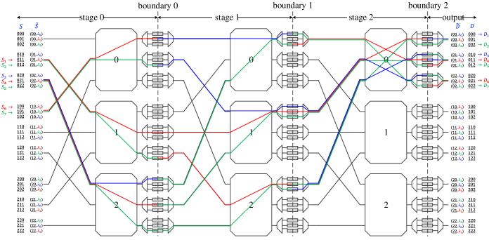
S=sn¯sn1¯s1¯shufflesn1¯s1¯sn¯exchangesn1¯s1¯dn¯shufflesnk1¯dnk+1¯snk¯exchangesnk1¯dnk+1¯dnk¯shuffledn¯dn1¯d2¯s1¯exchangedn¯dn1¯d2¯d1¯=D.𝑆¯absentsubscript𝑠𝑛¯absentsubscript𝑠𝑛1¯absentsubscript𝑠1shuffle¯absentsubscript𝑠𝑛1¯absentsubscript𝑠1¯absentsubscript𝑠𝑛exchange¯absentsubscript𝑠𝑛1¯absentsubscript𝑠1¯absentsubscript𝑑𝑛shuffle¯absentsubscript𝑠𝑛𝑘1¯absentsubscript𝑑𝑛𝑘1¯absentsubscript𝑠𝑛𝑘exchange¯absentsubscript𝑠𝑛𝑘1¯absentsubscript𝑑𝑛𝑘1¯absentsubscript𝑑𝑛𝑘shuffle¯absentsubscript𝑑𝑛¯absentsubscript𝑑𝑛1¯absentsubscript𝑑2¯absentsubscript𝑠1exchange¯absentsubscript𝑑𝑛¯absentsubscript𝑑𝑛1¯absentsubscript𝑑2¯absentsubscript𝑑1𝐷{\begin{split}S=\underaccent{{\underline{\mskip 19.0mu}}}{{s_{n}}}\underaccent{{\underline{\mskip 41.0mu}}}{{s_{n-1}}}\cdots&\underaccent{{\underline{\mskip 19.0mu}}}{{s_{1}}}\\ \xrightarrow[]{\scriptsize\mbox{shuffle}}\underaccent{{\underline{\mskip 38.0mu}}}{{s_{n-1}}}\cdots\underaccent{{\underline{\mskip 17.0mu}}}{{s_{1}}}&\underaccent{{\underline{\mskip 17.0mu}}}{{s_{n}}}\xrightarrow[]{\scriptsize\mbox{exchange}}\underaccent{{\underline{\mskip 38.0mu}}}{{s_{n-1}}}\cdots\underaccent{{\underline{\mskip 17.0mu}}}{{s_{1}}}\underaccent{{\underline{\mskip 17.0mu}}}{{d_{n}}}\\ &\cdots\\ \xrightarrow[]{\scriptsize\mbox{shuffle}}\underaccent{{\underline{\mskip 63.0mu}}}{{s_{n-k-1}}}\cdots&\underaccent{{\underline{\mskip 63.0mu}}}{{d_{n-k+1}}}\underaccent{{\underline{\mskip 38.0mu}}}{{s_{n-k}}}\xrightarrow[]{\scriptsize\mbox{exchange}}\underaccent{{\underline{\mskip 63.0mu}}}{{s_{n-k-1}}}\cdots\underaccent{{\underline{\mskip 63.0mu}}}{{d_{n-k+1}}}\underaccent{{\underline{\mskip 38.0mu}}}{{d_{n-k}}}\\ &\cdots\\ \xrightarrow[]{\scriptsize\mbox{shuffle}}\underaccent{{\underline{\mskip 17.0mu}}}{{d_{n}}}\underaccent{{\underline{\mskip 38.0mu}}}{{d_{n-1}}}\cdots&\underaccent{{\underline{\mskip 17.0mu}}}{{d_{2}}}\underaccent{{\underline{\mskip 17.0mu}}}{{s_{1}}}\xrightarrow[]{\scriptsize\mbox{exchange}}\underaccent{{\underline{\mskip 17.0mu}}}{{d_{n}}}\underaccent{{\underline{\mskip 38.0mu}}}{{d_{n-1}}}\cdots\underaccent{{\underline{\mskip 17.0mu}}}{{d_{2}}}\underaccent{{\underline{\mskip 17.0mu}}}{{d_{1}}}=D.\end{split}}
Refer to caption
Figure 8: Route of multi-requests without contention in 𝒮(3,3)𝒮33\mathcal{S}(3,3).

Also, for a set of requests π={R1,R2,,Rl}𝜋subscript𝑅1subscript𝑅2subscript𝑅𝑙\pi=\{R_{1},R_{2},\cdots,R_{l}\} arriving at the network, where lmn𝑙superscript𝑚𝑛l\leq m^{n}, the routing is nonblocking if π𝜋\pi satisfies the following two conditions [15]:

  1. 1)

    Monotonic: for Sj>Sisubscript𝑆𝑗subscript𝑆𝑖S_{j}>S_{i} if j>i𝑗𝑖j>i, there is D1<D2<<Dnsubscript𝐷1subscript𝐷2subscript𝐷𝑛D_{1}<D_{2}<\cdots<D_{n} or D1>D2>>Dnsubscript𝐷1subscript𝐷2subscript𝐷𝑛D_{1}>D_{2}>\cdots>D_{n}.

  2. 2)

    Concentrated: any input Sksubscript𝑆𝑘S_{k} between two active inputs Sisubscript𝑆𝑖S_{i} and Sjsubscript𝑆𝑗S_{j} is active.

R1:S~=(0¯1¯,λ1)S=0¯1¯1¯𝒲0(1¯1¯,λ1)1¯1¯0¯boundary 0(1¯1¯,λ1)1¯1¯0¯𝒲1(1¯0¯,λ1)1¯0¯1¯boundary 1(𝟏¯𝟎¯,𝝀𝟏)𝟏¯𝟎¯𝟎¯𝓦𝟐(𝟎¯𝟎¯,𝝀𝟏)𝟎¯𝟎¯𝟏¯boundary 2(0¯0¯,λ0)=D~0¯0¯0¯=D:subscript𝑅1subscript𝒲0~𝑆¯absent0¯absent1subscript𝜆1𝑆¯absent0¯absent1¯absent1¯absent1¯absent1subscript𝜆1¯absent1¯absent1¯absent0boundary 0¯absent1¯absent1subscript𝜆1¯absent1¯absent1¯absent0subscript𝒲1¯absent1¯absent0subscript𝜆1¯absent1¯absent0¯absent1boundary 1¯absent1¯absent0subscript𝝀1¯absent1¯absent0¯absent0subscript𝓦2¯absent0¯absent0subscript𝝀1¯absent0¯absent0¯absent1boundary 2¯absent0¯absent0subscript𝜆0~𝐷¯absent0¯absent0¯absent0𝐷R_{1}:{\begin{split}\tilde{S}=(\underaccent{{\underline{\mskip 7.0mu}}}{0}\underaccent{{\underline{\mskip 7.0mu}}}{1}&,\lambda_{1})\\ S=\underaccent{{\underline{\mskip 7.0mu}}}{0}&\underaccent{{\underline{\mskip 7.0mu}}}{1}\underaccent{{\underline{\mskip 7.0mu}}}{1}\end{split}}\xrightarrow[]{\mathcal{W}_{0}}{\begin{split}(\underaccent{{\underline{\mskip 7.0mu}}}{1}\underaccent{{\underline{\mskip 7.0mu}}}{1}&,\lambda_{1})\\ \underaccent{{\underline{\mskip 7.0mu}}}{1}&\underaccent{{\underline{\mskip 7.0mu}}}{1}\underaccent{{\underline{\mskip 7.0mu}}}{0}\end{split}}\xrightarrow[]{\mbox{boundary\ 0}}{\begin{split}(\underaccent{{\underline{\mskip 7.0mu}}}{1}\underaccent{{\underline{\mskip 7.0mu}}}{1}&,\lambda_{1})\\ \underaccent{{\underline{\mskip 7.0mu}}}{1}&\underaccent{{\underline{\mskip 7.0mu}}}{1}\underaccent{{\underline{\mskip 7.0mu}}}{0}\end{split}}\xrightarrow[]{\mathcal{W}_{1}}{\begin{split}(\underaccent{{\underline{\mskip 7.0mu}}}{1}\underaccent{{\underline{\mskip 7.0mu}}}{0}&,\lambda_{1})\\ \underaccent{{\underline{\mskip 7.0mu}}}{1}&\underaccent{{\underline{\mskip 7.0mu}}}{0}\underaccent{{\underline{\mskip 7.0mu}}}{1}\end{split}}\xrightarrow[]{\mbox{boundary\ 1}}{\begin{split}(\underaccent{{\underline{\mskip 7.0mu}}}{\bm{1}}\underaccent{{\underline{\mskip 7.0mu}}}{\bm{0}}&,\bm{\lambda_{1}})\\ \underaccent{{\underline{\mskip 7.0mu}}}{\bm{1}}&\underaccent{{\underline{\mskip 7.0mu}}}{\bm{0}}\underaccent{{\underline{\mskip 7.0mu}}}{\bm{0}}\end{split}}\xrightarrow[]{\bm{\mathcal{W}_{2}}}{\begin{split}(\underaccent{{\underline{\mskip 7.0mu}}}{\bm{0}}\underaccent{{\underline{\mskip 7.0mu}}}{\bm{0}}&,\bm{\lambda_{1}})\\ \underaccent{{\underline{\mskip 7.0mu}}}{\bm{0}}&\underaccent{{\underline{\mskip 7.0mu}}}{\bm{0}}\underaccent{{\underline{\mskip 7.0mu}}}{\bm{1}}\end{split}}\xrightarrow[]{\mbox{boundary\ 2}}{\begin{split}(\underaccent{{\underline{\mskip 7.0mu}}}{0}\underaccent{{\underline{\mskip 7.0mu}}}{0},&\lambda_{0})=\tilde{D}\\ \underaccent{{\underline{\mskip 7.0mu}}}{0}\underaccent{{\underline{\mskip 7.0mu}}}{0}&\underaccent{{\underline{\mskip 7.0mu}}}{0}=D\end{split}} (17)
R2:S~=(1¯0¯,λ2)S=1¯0¯1¯𝒲0(0¯1¯,λ2)0¯1¯1¯boundary 0(0¯1¯,λ0)0¯1¯0¯𝒲1(1¯0¯,λ0)1¯0¯0¯boundary 1(𝟏¯𝟎¯,𝝀𝟏)𝟏¯𝟎¯𝟎¯𝓦𝟐(𝟎¯𝟎¯,𝝀𝟏)𝟎¯𝟎¯𝟏¯boundary 2(0¯0¯,λ2)=D~0¯0¯2¯=D:subscript𝑅2subscript𝒲0~𝑆¯absent1¯absent0subscript𝜆2𝑆¯absent1¯absent0¯absent1¯absent0¯absent1subscript𝜆2¯absent0¯absent1¯absent1boundary 0¯absent0¯absent1subscript𝜆0¯absent0¯absent1¯absent0subscript𝒲1¯absent1¯absent0subscript𝜆0¯absent1¯absent0¯absent0boundary 1¯absent1¯absent0subscript𝝀1¯absent1¯absent0¯absent0subscript𝓦2¯absent0¯absent0subscript𝝀1¯absent0¯absent0¯absent1boundary 2¯absent0¯absent0subscript𝜆2~𝐷¯absent0¯absent0¯absent2𝐷R_{2}:{\begin{split}\tilde{S}=(\underaccent{{\underline{\mskip 7.0mu}}}{1}\underaccent{{\underline{\mskip 7.0mu}}}{0}&,\lambda_{2})\\ S=\underaccent{{\underline{\mskip 7.0mu}}}{1}&\underaccent{{\underline{\mskip 7.0mu}}}{0}\underaccent{{\underline{\mskip 7.0mu}}}{1}\end{split}}\xrightarrow[]{\mathcal{W}_{0}}{\begin{split}(\underaccent{{\underline{\mskip 7.0mu}}}{0}\underaccent{{\underline{\mskip 7.0mu}}}{1}&,\lambda_{2})\\ \underaccent{{\underline{\mskip 7.0mu}}}{0}&\underaccent{{\underline{\mskip 7.0mu}}}{1}\underaccent{{\underline{\mskip 7.0mu}}}{1}\end{split}}\xrightarrow[]{\mbox{boundary\ 0}}{\begin{split}(\underaccent{{\underline{\mskip 7.0mu}}}{0}\underaccent{{\underline{\mskip 7.0mu}}}{1}&,\lambda_{0})\\ \underaccent{{\underline{\mskip 7.0mu}}}{0}&\underaccent{{\underline{\mskip 7.0mu}}}{1}\underaccent{{\underline{\mskip 7.0mu}}}{0}\end{split}}\xrightarrow[]{\mathcal{W}_{1}}{\begin{split}(\underaccent{{\underline{\mskip 7.0mu}}}{1}\underaccent{{\underline{\mskip 7.0mu}}}{0}&,\lambda_{0})\\ \underaccent{{\underline{\mskip 7.0mu}}}{1}&\underaccent{{\underline{\mskip 7.0mu}}}{0}\underaccent{{\underline{\mskip 7.0mu}}}{0}\end{split}}\xrightarrow[]{\mbox{boundary\ 1}}{\begin{split}(\underaccent{{\underline{\mskip 7.0mu}}}{\bm{1}}\underaccent{{\underline{\mskip 7.0mu}}}{\bm{0}}&,\bm{\lambda_{1}})\\ \underaccent{{\underline{\mskip 7.0mu}}}{\bm{1}}&\underaccent{{\underline{\mskip 7.0mu}}}{\bm{0}}\underaccent{{\underline{\mskip 7.0mu}}}{\bm{0}}\end{split}}\xrightarrow[]{\bm{\mathcal{W}_{2}}}{\begin{split}(\underaccent{{\underline{\mskip 7.0mu}}}{\bm{0}}\underaccent{{\underline{\mskip 7.0mu}}}{\bm{0}}&,\bm{\lambda_{1}})\\ \underaccent{{\underline{\mskip 7.0mu}}}{\bm{0}}&\underaccent{{\underline{\mskip 7.0mu}}}{\bm{0}}\underaccent{{\underline{\mskip 7.0mu}}}{\bm{1}}\end{split}}\xrightarrow[]{\mbox{boundary\ 2}}{\begin{split}(\underaccent{{\underline{\mskip 7.0mu}}}{0}\underaccent{{\underline{\mskip 7.0mu}}}{0},&\lambda_{2})=\tilde{D}\\ \underaccent{{\underline{\mskip 7.0mu}}}{0}\underaccent{{\underline{\mskip 7.0mu}}}{0}&\underaccent{{\underline{\mskip 7.0mu}}}{2}=D\end{split}} (18)

As a kind of WDM switching network, the process that 𝒮(m,n)𝒮𝑚𝑛\mathcal{S}(m,n) sets up connections for the requests possesses its own feature. Both routing assignment and wavelength assignment should be taken into consideration during connection establishment, which is known as routing and wavelength assignment (RWA) problem. In such kind of network, there is a fundamental condition for contention-free RWA [31]: if two connections share the same link, they must use different wavelengths; otherwise, they must be link-disjoint. In other words, there is a contention if two connections use the same wavelength at the same link. Though there exist differences between the nonblocking routing in classical SENs and the contention-free RWA in AWG-based WDM SENs, we show in this section that the self-routing property and nonblocking conditions still hold in such WDM SENs.

V-A Self-routing property of 𝒲(m,n)𝒲𝑚𝑛\mathcal{W}(m,n)

To illustrate the self-routing property of 𝒮(m,n)𝒮𝑚𝑛\mathcal{S}(m,n), we take connection R(0¯1¯0¯,1¯1¯1¯)𝑅¯absent0¯absent1¯absent0¯absent1¯absent1¯absent1R(\underaccent{{\underline{\mskip 7.0mu}}}{0}\underaccent{{\underline{\mskip 7.0mu}}}{1}\underaccent{{\underline{\mskip 7.0mu}}}{0},\underaccent{{\underline{\mskip 7.0mu}}}{1}\underaccent{{\underline{\mskip 7.0mu}}}{1}\underaccent{{\underline{\mskip 7.0mu}}}{1}) in Fig. 6 as an example. The two-tuple address of S=0¯1¯0¯𝑆¯absent0¯absent1¯absent0S=\underaccent{{\underline{\mskip 7.0mu}}}{0}\underaccent{{\underline{\mskip 7.0mu}}}{1}\underaccent{{\underline{\mskip 7.0mu}}}{0} is S~=(0¯1¯,λ0)~𝑆¯absent0¯absent1subscript𝜆0\tilde{S}=(\underaccent{{\underline{\mskip 7.0mu}}}{0}\underaccent{{\underline{\mskip 7.0mu}}}{1},\lambda_{0}), and that of D=1¯1¯1¯𝐷¯absent1¯absent1¯absent1D=\underaccent{{\underline{\mskip 7.0mu}}}{1}\underaccent{{\underline{\mskip 7.0mu}}}{1}\underaccent{{\underline{\mskip 7.0mu}}}{1} is D~=(1¯1¯,λ2)~𝐷¯absent1¯absent1subscript𝜆2\tilde{D}=(\underaccent{{\underline{\mskip 7.0mu}}}{1}\underaccent{{\underline{\mskip 7.0mu}}}{1},\lambda_{2}). According to the connection property of 𝒲0(3,32)subscript𝒲03superscript32\mathcal{W}_{0}(3,3^{2}), S𝑆S links to

Y0=s1¯s0¯s2¯=1¯0¯0¯subscript𝑌0¯absentsubscript𝑠1¯absentsubscript𝑠0¯absentsubscript𝑠2¯absent1¯absent0¯absent0Y_{0}=\underaccent{{\underline{\mskip 19.0mu}}}{{s_{1}}}\underaccent{{\underline{\mskip 19.0mu}}}{{s_{0}}}\underaccent{{\underline{\mskip 19.0mu}}}{{s_{2}}}=\underaccent{{\underline{\mskip 7.0mu}}}{1}\underaccent{{\underline{\mskip 7.0mu}}}{0}\underaccent{{\underline{\mskip 7.0mu}}}{0}

or

Y~0=(s1¯s0¯,λ[s0+s2]3)=(1¯0¯,λ0).subscript~𝑌0¯absentsubscript𝑠1¯absentsubscript𝑠0subscript𝜆subscriptdelimited-[]subscript𝑠0subscript𝑠23¯absent1¯absent0subscript𝜆0\tilde{Y}_{0}=(\underaccent{{\underline{\mskip 19.0mu}}}{{s_{1}}}\underaccent{{\underline{\mskip 19.0mu}}}{{s_{0}}},\lambda_{[s_{0}+s_{2}]_{3}})=(\underaccent{{\underline{\mskip 7.0mu}}}{1}\underaccent{{\underline{\mskip 7.0mu}}}{0},\lambda_{0}).

Following the self-routing property, wavelength boundary 00 switches Y0subscript𝑌0Y_{0} to

X1=s1¯s0¯d2¯=1¯0¯1¯subscript𝑋1¯absentsubscript𝑠1¯absentsubscript𝑠0¯absentsubscript𝑑2¯absent1¯absent0¯absent1X_{1}=\underaccent{{\underline{\mskip 19.0mu}}}{{s_{1}}}\underaccent{{\underline{\mskip 19.0mu}}}{{s_{0}}}\underaccent{{\underline{\mskip 19.0mu}}}{{d_{2}}}=\underaccent{{\underline{\mskip 7.0mu}}}{1}\underaccent{{\underline{\mskip 7.0mu}}}{0}\underaccent{{\underline{\mskip 7.0mu}}}{1}

or

X~1=(s1¯s0¯,λ[s0+d2]3)=(1¯0¯,λ1),subscript~𝑋1¯absentsubscript𝑠1¯absentsubscript𝑠0subscript𝜆subscriptdelimited-[]subscript𝑠0subscript𝑑23¯absent1¯absent0subscript𝜆1\tilde{X}_{1}=(\underaccent{{\underline{\mskip 19.0mu}}}{{s_{1}}}\underaccent{{\underline{\mskip 19.0mu}}}{{s_{0}}},\lambda_{[s_{0}+d_{2}]_{3}})=(\underaccent{{\underline{\mskip 7.0mu}}}{1}\underaccent{{\underline{\mskip 7.0mu}}}{0},\lambda_{1}),

meaning that boundary 00 changes the wavelength from λ0subscript𝜆0\lambda_{0} to λ1subscript𝜆1\lambda_{1}. By analogy, R𝑅R passes through the wavelength channels along the path given by (16).

It is shown by (16) that R𝑅R passes through a wavelength boundary using one field of D𝐷D, and finally reaches the destination wavelength channel D𝐷D. This example clearly demonstrates that 𝒮(m,n)𝒮𝑚𝑛\mathcal{S}(m,n) also possesses the self-routing property.

Table V gives the routing process of R𝑅R in general case. In particular, at the k𝑘kth shuffle stage 𝒲ksubscript𝒲𝑘\mathcal{W}_{k}, connection R𝑅R travels from

Xk=snk¯dnk+2¯dnk+1¯subscript𝑋𝑘¯absentsubscript𝑠𝑛𝑘¯absentsubscript𝑑𝑛𝑘2¯absentsubscript𝑑𝑛𝑘1X_{k}=\underaccent{{\underline{\mskip 41.0mu}}}{{s_{n-k}}}\cdots\underaccent{{\underline{\mskip 66.0mu}}}{{d_{n-k+2}}}\underaccent{{\underline{\mskip 66.0mu}}}{{d_{n-k+1}}}

or

X~k=(snk¯dnk+2¯,λik)subscript~𝑋𝑘¯absentsubscript𝑠𝑛𝑘¯absentsubscript𝑑𝑛𝑘2subscript𝜆subscript𝑖𝑘\tilde{X}_{k}=(\underaccent{{\underline{\mskip 41.0mu}}}{{s_{n-k}}}\cdots\underaccent{{\underline{\mskip 71.0mu}}}{{d_{n-k+2}}},\lambda_{i_{k}})

to

Yk=snk1¯dnk+1¯snk¯subscript𝑌𝑘¯absentsubscript𝑠𝑛𝑘1¯absentsubscript𝑑𝑛𝑘1¯absentsubscript𝑠𝑛𝑘Y_{k}=\underaccent{{\underline{\mskip 66.0mu}}}{{s_{n-k-1}}}\cdots\underaccent{{\underline{\mskip 66.0mu}}}{{d_{n-k+1}}}\underaccent{{\underline{\mskip 41.0mu}}}{{s_{n-k}}}

or

Y~k=(snk1¯dnk+1¯,λik),subscript~𝑌𝑘¯absentsubscript𝑠𝑛𝑘1¯absentsubscript𝑑𝑛𝑘1subscript𝜆subscript𝑖𝑘\tilde{Y}_{k}=(\underaccent{{\underline{\mskip 66.0mu}}}{{s_{n-k-1}}}\cdots\underaccent{{\underline{\mskip 71.0mu}}}{{d_{n-k+1}}},\lambda_{i_{k}}),

where

ik=[snk+dnk+1]m,subscript𝑖𝑘subscriptdelimited-[]subscript𝑠𝑛𝑘subscript𝑑𝑛𝑘1𝑚i_{k}=[s_{n-k}+d_{n-k+1}]_{m},

and the wavelength of R𝑅R is converted from

λik=λ[snk+dnk+1]msubscript𝜆subscript𝑖𝑘subscript𝜆subscriptdelimited-[]subscript𝑠𝑛𝑘subscript𝑑𝑛𝑘1𝑚\lambda_{i_{k}}=\lambda_{[s_{n-k}+d_{n-k+1}]_{m}}

to

λik+1=λ[snk1+dnk]msubscript𝜆subscript𝑖𝑘1subscript𝜆subscriptdelimited-[]subscript𝑠𝑛𝑘1subscript𝑑𝑛𝑘𝑚\lambda_{i_{k+1}}=\lambda_{[s_{n-k-1}+d_{n-k}]_{m}}

at the k𝑘kth wavelength exchange boundary.

V-B Nonblocking Self-Routing Conditions

If there exist multiple requests in 𝒮(m,n)𝒮𝑚𝑛\mathcal{S}(m,n) at the same time, wavelength contentions may happen. To see this point, suppose there are two connection requests R1(0¯1¯1¯,0¯0¯0¯)subscript𝑅1¯absent0¯absent1¯absent1¯absent0¯absent0¯absent0R_{1}(\underaccent{{\underline{\mskip 7.0mu}}}{0}\underaccent{{\underline{\mskip 7.0mu}}}{1}\underaccent{{\underline{\mskip 7.0mu}}}{1},\underaccent{{\underline{\mskip 7.0mu}}}{0}\underaccent{{\underline{\mskip 7.0mu}}}{0}\underaccent{{\underline{\mskip 7.0mu}}}{0}) and R2(1¯0¯1¯,0¯0¯2¯)subscript𝑅2¯absent1¯absent0¯absent1¯absent0¯absent0¯absent2R_{2}(\underaccent{{\underline{\mskip 7.0mu}}}{1}\underaccent{{\underline{\mskip 7.0mu}}}{0}\underaccent{{\underline{\mskip 7.0mu}}}{1},\underaccent{{\underline{\mskip 7.0mu}}}{0}\underaccent{{\underline{\mskip 7.0mu}}}{0}\underaccent{{\underline{\mskip 7.0mu}}}{2}) arriving at S~(3,3)~𝑆33\tilde{S}(3,3). According to the self-routing property, the RWAs of R1subscript𝑅1R_{1} and R2subscript𝑅2R_{2} will respectively be (17) and (18).

In other words, they will have wavelength contention at the input of shuffle stage 𝒲2subscript𝒲2\mathcal{W}_{2}, since their wavelengths will both be converted to λ1subscript𝜆1\lambda_{1} at boundary 111. From this example, we conclude that:

  1. 1)

    Wavelength contention may happen if there exist multiple requests;

  2. 2)

    A contention may happen at an input of a shuffle stage.

The contention will not happen at an output of a shuffle stage if two requests do not use the same wavelength at the same input of a shuffle stage, since each shuffle stage is wavelength contention-free as Property 2 in Section III shows. This implies that the RWA will be contention-free if any two requests do not use the same wavelength at an input of a shuffle stage.

In the following, we show that the RWA can be contention-free if the set of requests π𝜋\pi satisfies the monotonic and concentrated conditions.

Theorem 1.

AWG-based WDM SEN 𝒮(m,n)𝒮𝑚𝑛\mathcal{S}(m,n) is contention-free if the requests in this network are monotonic and concentrated.

Proof:

Consider two requests R(S,D)𝑅𝑆𝐷R(S,D) and R(S,D)superscript𝑅superscript𝑆superscript𝐷R^{\prime}(S^{\prime},D^{\prime}), where

S=sn¯s2¯s1¯>S=sn¯s2¯s1¯superscript𝑆¯absentsuperscriptsubscript𝑠𝑛¯absentsuperscriptsubscript𝑠2¯absentsuperscriptsubscript𝑠1𝑆¯absentsubscript𝑠𝑛¯absentsubscript𝑠2¯absentsubscript𝑠1{S^{\prime}=\underaccent{{\underline{\mskip 19.0mu}}}{{s_{n}^{\prime}}}\cdots\underaccent{{\underline{\mskip 19.0mu}}}{{s_{2}^{\prime}}}\underaccent{{\underline{\mskip 19.0mu}}}{{s_{1}^{\prime}}}>S=\underaccent{{\underline{\mskip 19.0mu}}}{{s_{n}}}\cdots\underaccent{{\underline{\mskip 19.0mu}}}{{s_{2}}}\underaccent{{\underline{\mskip 19.0mu}}}{{s_{1}}}} (19)

and

D=dn¯d2¯d1¯>D=dn¯d2¯d1¯.superscript𝐷¯absentsuperscriptsubscript𝑑𝑛¯absentsuperscriptsubscript𝑑2¯absentsuperscriptsubscript𝑑1𝐷¯absentsubscript𝑑𝑛¯absentsubscript𝑑2¯absentsubscript𝑑1{D^{\prime}=\underaccent{{\underline{\mskip 19.0mu}}}{{d_{n}^{\prime}}}\cdots\underaccent{{\underline{\mskip 19.0mu}}}{{d_{2}^{\prime}}}\underaccent{{\underline{\mskip 19.0mu}}}{{d_{1}^{\prime}}}>D=\underaccent{{\underline{\mskip 19.0mu}}}{{d_{n}}}\cdots\underaccent{{\underline{\mskip 19.0mu}}}{{d_{2}}}\underaccent{{\underline{\mskip 19.0mu}}}{{d_{1}}}.} (20)

The number of input channels between S𝑆S and Ssuperscript𝑆S^{\prime} is |SS+1|superscript𝑆𝑆1|S^{\prime}-S+1|, and that of output channels between D𝐷D and Dsuperscript𝐷D^{\prime} is |DD+1|superscript𝐷𝐷1|D^{\prime}-D+1|. It follows from the concentrated condition

|SS||DD|.superscript𝑆𝑆superscript𝐷𝐷{|S^{\prime}-S|\leq|D^{\prime}-D|.} (21)

According to the self-routing property, R𝑅R and Rsuperscript𝑅R^{\prime} respectively reach the output wavelength channel of 𝒲ksubscript𝒲𝑘\mathcal{W}_{k} as follows:

Yk=snk1¯dnk+1¯snk¯subscript𝑌𝑘¯absentsubscript𝑠𝑛𝑘1¯absentsubscript𝑑𝑛𝑘1¯absentsubscript𝑠𝑛𝑘{Y_{k}=\underaccent{{\underline{\mskip 63.0mu}}}{{s_{n-k-1}}}\cdots\underaccent{{\underline{\mskip 63.0mu}}}{{d_{n-k+1}}}\underaccent{{\underline{\mskip 41.0mu}}}{{s_{n-k}}}} (22)

or

Y~k=(snk1¯dnk+1¯,λi),subscript~𝑌𝑘¯absentsubscript𝑠𝑛𝑘1¯absentsubscript𝑑𝑛𝑘1subscript𝜆𝑖{\tilde{Y}_{k}=(\underaccent{{\underline{\mskip 63.0mu}}}{{s_{n-k-1}}}\cdots\underaccent{{\underline{\mskip 63.0mu}}}{{d_{n-k+1}}},\lambda_{i}),} (23)

and

Yk=snk1¯dnk+1¯snk¯subscriptsuperscript𝑌𝑘¯absentsubscriptsuperscript𝑠𝑛𝑘1¯absentsubscriptsuperscript𝑑𝑛𝑘1¯absentsubscriptsuperscript𝑠𝑛𝑘{Y^{\prime}_{k}=\underaccent{{\underline{\mskip 63.0mu}}}{{s^{\prime}_{n-k-1}}}\cdots\underaccent{{\underline{\mskip 63.0mu}}}{{d^{\prime}_{n-k+1}}}\underaccent{{\underline{\mskip 41.0mu}}}{{s^{\prime}_{n-k}}}} (24)

or

Y~k=(snk1¯dnk+1¯,λi),subscriptsuperscript~𝑌𝑘¯absentsubscriptsuperscript𝑠𝑛𝑘1¯absentsubscriptsuperscript𝑑𝑛𝑘1subscript𝜆superscript𝑖{\tilde{Y}^{\prime}_{k}=(\underaccent{{\underline{\mskip 63.0mu}}}{{s^{\prime}_{n-k-1}}}\cdots\underaccent{{\underline{\mskip 63.0mu}}}{{d^{\prime}_{n-k+1}}},\lambda_{i^{\prime}}),} (25)

where

i=[snk+dnk+1]m𝑖subscriptdelimited-[]subscript𝑠𝑛𝑘subscript𝑑𝑛𝑘1𝑚{i=[s_{n-k}+d_{n-k+1}]_{m}} (26)

and

i=[snk+dnk+1]m.superscript𝑖subscriptdelimited-[]subscriptsuperscript𝑠𝑛𝑘subscriptsuperscript𝑑𝑛𝑘1𝑚{i^{\prime}=[s^{\prime}_{n-k}+d^{\prime}_{n-k+1}]_{m}.} (27)

Assume that R𝑅R and Rsuperscript𝑅R^{\prime} compete for the same input wavelength channel of 𝒲k+1subscript𝒲𝑘1\mathcal{W}_{k+1}. In this case, they first reach different output wavelength channels of 𝒲ksubscript𝒲𝑘\mathcal{W}_{k}, which means

snk1¯dnk+1¯=snk1¯dnk+1¯¯absentsubscript𝑠𝑛𝑘1¯absentsubscript𝑑𝑛𝑘1¯absentsubscriptsuperscript𝑠𝑛𝑘1¯absentsubscriptsuperscript𝑑𝑛𝑘1{\underaccent{{\underline{\mskip 68.0mu}}}{{s_{n-k-1}}}\cdots\underaccent{{\underline{\mskip 68.0mu}}}{{d_{n-k+1}}}=\underaccent{{\underline{\mskip 68.0mu}}}{{s^{\prime}_{n-k-1}}}\cdots\underaccent{{\underline{\mskip 68.0mu}}}{{d^{\prime}_{n-k+1}}}} (28)

and

snksnk.subscript𝑠𝑛𝑘subscriptsuperscript𝑠𝑛𝑘{s_{n-k}\not=s^{\prime}_{n-k}.} (29)

According to dnksubscript𝑑𝑛𝑘d_{n-k} and dnksubscriptsuperscript𝑑𝑛𝑘d^{\prime}_{n-k}, boundary k𝑘k then converts R𝑅R and Rsuperscript𝑅R^{\prime} respectively to the same input wavelength channel of 𝒲k+1subscript𝒲𝑘1\mathcal{W}_{k+1}, i.e.,

where λjsubscript𝜆𝑗\lambda_{j} denotes the wavelength of input channel. Thus, we have

dnk=[jsnk1]m=[jsnk1]m=dnk.subscript𝑑𝑛𝑘subscriptdelimited-[]𝑗subscript𝑠𝑛𝑘1𝑚subscriptdelimited-[]𝑗subscriptsuperscript𝑠𝑛𝑘1𝑚subscriptsuperscript𝑑𝑛𝑘{d_{n-k}=[j-s_{n-k-1}]_{m}=[j-s^{\prime}_{n-k-1}]_{m}=d^{\prime}_{n-k}.} (30)

According to (28)-(30), we have

|SS|=|sn¯s1¯sn¯s1¯|=|sn¯snk¯0¯0¯||sn¯snk¯0¯0¯|=|sn¯snk¯sn¯snk¯|×mnk1mnk1superscript𝑆𝑆¯absentsubscriptsuperscript𝑠𝑛¯absentsubscriptsuperscript𝑠1¯absentsubscript𝑠𝑛¯absentsubscript𝑠1¯absentsubscriptsuperscript𝑠𝑛¯absentsubscriptsuperscript𝑠𝑛𝑘¯absent0¯absent0¯absentsubscript𝑠𝑛¯absentsubscript𝑠𝑛𝑘¯absent0¯absent0¯absentsubscriptsuperscript𝑠𝑛¯absentsubscriptsuperscript𝑠𝑛𝑘¯absentsubscript𝑠𝑛¯absentsubscript𝑠𝑛𝑘superscript𝑚𝑛𝑘1superscript𝑚𝑛𝑘1\small{\begin{split}|S^{\prime}-S|&=|\underaccent{{\underline{\mskip 19.0mu}}}{{s^{\prime}_{n}}}\cdots\underaccent{{\underline{\mskip 19.0mu}}}{{s^{\prime}_{1}}}-\underaccent{{\underline{\mskip 19.0mu}}}{{s_{n}}}\cdots\underaccent{{\underline{\mskip 19.0mu}}}{{s_{1}}}|\\ &=|\underaccent{{\underline{\mskip 19.0mu}}}{{s^{\prime}_{n}}}\cdots\underaccent{{\underline{\mskip 45.0mu}}}{{s^{\prime}_{n-k}}}\underaccent{{\underline{\mskip 7.0mu}}}{0}\cdots\underaccent{{\underline{\mskip 7.0mu}}}{0}|-|\underaccent{{\underline{\mskip 19.0mu}}}{{s_{n}}}\cdots\underaccent{{\underline{\mskip 45.0mu}}}{{s_{n-k}}}\underaccent{{\underline{\mskip 7.0mu}}}{0}\cdots\underaccent{{\underline{\mskip 7.0mu}}}{0}|\\ &=|\underaccent{{\underline{\mskip 19.0mu}}}{{s^{\prime}_{n}}}\cdots\underaccent{{\underline{\mskip 45.0mu}}}{{s^{\prime}_{n-k}}}-\underaccent{{\underline{\mskip 19.0mu}}}{{s_{n}}}\cdots\underaccent{{\underline{\mskip 45.0mu}}}{{s_{n-k}}}|\times m^{n-k-1}\\ &\geq m^{n-k-1}\end{split}}

and

|DD|=|dn¯d1¯||dn¯d1¯|=|0¯0¯dnk1¯d1¯||0¯0¯dnk1¯d1¯|mnk11,superscript𝐷𝐷¯absentsubscriptsuperscript𝑑𝑛¯absentsubscriptsuperscript𝑑1¯absentsubscript𝑑𝑛¯absentsubscript𝑑1¯absent0¯absent0¯absentsubscriptsuperscript𝑑𝑛𝑘1¯absentsubscriptsuperscript𝑑1¯absent0¯absent0¯absentsubscript𝑑𝑛𝑘1¯absentsubscript𝑑1superscript𝑚𝑛𝑘11\small{\begin{split}|D^{\prime}-D|&=|\underaccent{{\underline{\mskip 19.0mu}}}{{d^{\prime}_{n}}}\cdots\underaccent{{\underline{\mskip 19.0mu}}}{{d^{\prime}_{1}}}|-|\underaccent{{\underline{\mskip 19.0mu}}}{{d_{n}}}\cdots\underaccent{{\underline{\mskip 19.0mu}}}{{d_{1}}}|\\ &=|\underaccent{{\underline{\mskip 7.0mu}}}{0}\cdots\underaccent{{\underline{\mskip 7.0mu}}}{0}\underaccent{{\underline{\mskip 68.0mu}}}{{d^{\prime}_{n-k-1}}}\cdots\underaccent{{\underline{\mskip 19.0mu}}}{{d^{\prime}_{1}}}|-|\underaccent{{\underline{\mskip 7.0mu}}}{0}\cdots\underaccent{{\underline{\mskip 7.0mu}}}{0}\underaccent{{\underline{\mskip 68.0mu}}}{{d_{n-k-1}}}\cdots\underaccent{{\underline{\mskip 19.0mu}}}{{d_{1}}}|\\ &\leq m^{n-k-1}-1,\end{split}}

which indicates

|SS|>|DD|.superscript𝑆𝑆superscript𝐷𝐷{|S^{\prime}-S|>|D^{\prime}-D|.} (31)

This contradicts (21). Therefore, R𝑅R and Rsuperscript𝑅R^{\prime} must not share the same input wavelength channel of 𝒲k+1subscript𝒲𝑘1\mathcal{W}_{k+1}.

As the two requests are arbitrarily chosen, the RWAs in the AWG-based WDM SEN are contention-free. ∎ Fig. 8 gives an example where the set of requests is as follows:

π={R1(0¯1¯1¯,0¯0¯0¯),R2(0¯1¯2¯,0¯0¯2¯)R3(0¯2¯0¯,0¯1¯0¯),R4(0¯2¯1¯,0¯1¯1¯),R5(0¯2¯2¯,0¯1¯2¯),R6(1¯0¯0¯,0¯2¯1¯),R7(1¯0¯1¯,0¯2¯2¯)}.{\begin{array}[]{c}\pi=\{R_{1}(\underaccent{{\underline{\mskip 7.0mu}}}{0}\underaccent{{\underline{\mskip 7.0mu}}}{1}\underaccent{{\underline{\mskip 7.0mu}}}{1},\underaccent{{\underline{\mskip 7.0mu}}}{0}\underaccent{{\underline{\mskip 7.0mu}}}{0}\underaccent{{\underline{\mskip 7.0mu}}}{0}),R_{2}(\underaccent{{\underline{\mskip 7.0mu}}}{0}\underaccent{{\underline{\mskip 7.0mu}}}{1}\underaccent{{\underline{\mskip 7.0mu}}}{2},\underaccent{{\underline{\mskip 7.0mu}}}{0}\underaccent{{\underline{\mskip 7.0mu}}}{0}\underaccent{{\underline{\mskip 7.0mu}}}{2})R_{3}(\underaccent{{\underline{\mskip 7.0mu}}}{0}\underaccent{{\underline{\mskip 7.0mu}}}{2}\underaccent{{\underline{\mskip 7.0mu}}}{0},\underaccent{{\underline{\mskip 7.0mu}}}{0}\underaccent{{\underline{\mskip 7.0mu}}}{1}\underaccent{{\underline{\mskip 7.0mu}}}{0}),R_{4}(\underaccent{{\underline{\mskip 7.0mu}}}{0}\underaccent{{\underline{\mskip 7.0mu}}}{2}\underaccent{{\underline{\mskip 7.0mu}}}{1},\underaccent{{\underline{\mskip 7.0mu}}}{0}\underaccent{{\underline{\mskip 7.0mu}}}{1}\underaccent{{\underline{\mskip 7.0mu}}}{1}),\\ R_{5}(\underaccent{{\underline{\mskip 7.0mu}}}{0}\underaccent{{\underline{\mskip 7.0mu}}}{2}\underaccent{{\underline{\mskip 7.0mu}}}{2},\underaccent{{\underline{\mskip 7.0mu}}}{0}\underaccent{{\underline{\mskip 7.0mu}}}{1}\underaccent{{\underline{\mskip 7.0mu}}}{2}),R_{6}(\underaccent{{\underline{\mskip 7.0mu}}}{1}\underaccent{{\underline{\mskip 7.0mu}}}{0}\underaccent{{\underline{\mskip 7.0mu}}}{0},\underaccent{{\underline{\mskip 7.0mu}}}{0}\underaccent{{\underline{\mskip 7.0mu}}}{2}\underaccent{{\underline{\mskip 7.0mu}}}{1}),R_{7}(\underaccent{{\underline{\mskip 7.0mu}}}{1}\underaccent{{\underline{\mskip 7.0mu}}}{0}\underaccent{{\underline{\mskip 7.0mu}}}{1},\underaccent{{\underline{\mskip 7.0mu}}}{0}\underaccent{{\underline{\mskip 7.0mu}}}{2}\underaccent{{\underline{\mskip 7.0mu}}}{2})\}.\end{array}} (34)

It is clear that π𝜋\pi satisfies the monotonic and concentrated conditions. We can see that there is no contention even if some requests might share the same fiber link. An example is that R1subscript𝑅1R_{1}, R4subscript𝑅4R_{4}, and R7subscript𝑅7R_{7} at an input of 𝒲2subscript𝒲2\mathcal{W}_{2} in Fig. 8 use different wavelengths.

Let’s consider an extreme case where all the mnsuperscript𝑚𝑛m^{n} input wavelength channels of 𝒮(m,n)𝒮𝑚𝑛\mathcal{S}(m,n) are busy. Recall that there are mnsuperscript𝑚𝑛m^{n} TWCs at each exchange stage and the shuffle network at each shuffle stage contains mnsuperscript𝑚𝑛m^{n} wavelength channels. Therefore, the network will achieve 100% utilization in this case.

VI Conclusion

In this paper, we propose a method to construct an AWG-based optical SEN. We first study the equivalence between a single AWG and a classical shuffle network, based on which we devise a systematic approach to design a large-scale AWG-based WDM shuffle network. Combining the AWG-based WDM shuffle networks and the TWC-modules, we obtain an AWG-based WDM SEN, which is scalable due to the following reasons. First, the wavelength granularity, the coherent crosstalk, and the conversion range of the TWCs in the network are small since the network only employs a set of small-size AWGs associated with the same wavelength set. Second, the cabling complexity at each shuffle stage is low. Third, the RWA in this network is consistent with that in classical SENs. Fourth, the network can achieve 100% utilization if the input wavelength channels are all busy. Fifth, signals are 3R regenerated from stage to stage, ensuring high scalability in terms of number of stages.

References

  • [1] M. Mehrnaz and M. Othman, “A cost-effective architecture for optical multistage interconnection network,” Journal of Networks, vol. 8, pp. 345–350, Feb. 2013.
  • [2] F. Mashhadi, A. Asaduzzaman, and M. F. Mridha, “A novel resource scheduling approach to improve the reliability of shuffle-exchange networks,” in Proc. IEEE icIVPR, Feb. 2017, pp. 1–6.
  • [3] A. Sharifi, R. Sabbaghi-Nadooshan, and H. Sarbazi-Azad, “The shuffle-exchange mesh topology for 3D NoCs,” in Proc. International Symposium on Parallel Architectures, Algorithms, and Networks (PAAP), May 2008, pp. 275–280.
  • [4] D. Lugones, K. Katrinis, G. Theodoropoulos, and M. Collier, “A reconfigurable, regular-topology cluster/datacenter network using commodity optical switches,” Future Generation Computer Systems, pp. 78–89, Apr. 2014.
  • [5] K. Ueda, Y. Mori, H. Hasegawa, and K. Sato, “Novel intra- and inter-datacenter converged network exploiting space- and wavelength-dimensional switches,” in Proc. OFC, Mar. 2017, pp. 1–3.
  • [6] H. W. Park, I. Y. Yeo, J. R. Lee, and H. Jang, “Study on big data center traffic management based on the separation of large-scale data stream,” in Proc. Conference on Innovative Mobile and Internet Services in Ubiquitous Computing, Jul. 2017, pp. 591–594.
  • [7] W. Miao, F. Yan, and N. Calabretta, “Towards petabit/s all-optical flat data center networks based on WDM optical cross-connect switches with flow control,” J. Lightw. Technol., vol. 34, pp. 4066–4075, Sep. 2016.
  • [8] G. Veselovsky and S. Ackarachalanonth, “Constructing transition matrices for routing BPC permutations on shuffle-exchange recirculating networks,” in Proc. International Conference on Digital Information and Communication Technology and it’s Applications (DICTAP), May 2012, pp. 378–382.
  • [9] M. Othman and T. D. S. R. M. Auzar, “The development of crosstalk-free scheduling algorithms for routing in optical multistage interconnection networks,” in Trends in Telecommunications Technologies.   IntechOpen, 2010, ch. 29.
  • [10] T. D. Shahida, M. Othman, and M. Khazani, “Integrating RLP and fast zero algorithm to improve routing performance in optical multistage interconnection networks,” in Proc. International Symposium on High Capacity Optical Networks and Enabling Technologies, Nov. 2008, pp. 34–38.
  • [11] S. Arya and Nipur, “Link and switch conflicts-free routing in optical multistage interconnection networks,” in Proc. International Conference on Next Generation Computing Technologies (NGCT), Sep. 2015, pp. 312–315.
  • [12] V. Kamchevska, A. K. Medhin, F. D. Ros, F. Ye, R. Asif, A. M. Fagertun, S. Ruepp, M. Berger, L. Dittmann, T. Morioka, L. K. Oxenløwe, and M. Galili, “Experimental demonstration of multidimensional switching nodes for all-optical data center networks,” J. Lightw. Technol., vol. 34, pp. 1837–1843, Apr. 2016.
  • [13] K. W. Wong and L. M. Cheng, “Optical omega network: a compact implementation technique,” Appl. Opt., vol. 34, no. 29, pp. 6648–6651, Oct. 1995.
  • [14] K. Sunil and V. V. Alexander, “On shortest path routing in single stage shuffle-exchange networks,” in Proc. Annual ACM Symposium on Parallel Algorithms and Architectures, May 1995, pp. 298–307.
  • [15] T. T. Lee and S. C. Liew, Principle of broadband switching and networking.   Wiley-Interscience, 2010.
  • [16] M. Abdullah, M. Othman, and R. Johari, “An improved simulated annealing algorithm to avoid crosstalk in optical omega network,” in Proc. International Conference on Computing Informatics, Jun. 2006, pp. 1–7.
  • [17] G. Maier, P. Valzasina, and A. Pattavina, “AWG-based shuffle-exchange optical-interconnection architecture,” in Proc. International Conference on Computer Communications and Networks (ICCCN), Jul. 2011, pp. 1–6.
  • [18] Y. Liu, E. Tangdiongga, Z. Li, H. de Waardt, A. M. J. Koonen, G. D. Khoe, X. Shu, I. Bennion, and H. J. S. Dorren, “Error-free 320-gb/s all-optical wavelength conversion using a single semiconductor optical amplifier,” J. Lightw. Technol., vol. 25, pp. 103–108, Jan. 2007.
  • [19] R. Gaudino, G. A. G. Castillo, F. Neri, and J. M. Finochietto, “Simple optical fabrics for scalable terabit packet switches,” in Proc. IEEE ICC, 2008, pp. 5331–5337.
  • [20] A. Pattavina and R. Zanzottera, “Non-blocking wdm switches based on arrayed waveguide grating and shared wavelength conversion,” in Proc. IEEE INFOCOM, Apr. 2006, pp. 1–11.
  • [21] G. Weichenberg, V. W. S. Chan, and M. Médard, “Design and analysis of optical flow-switched networks,” IEEE J. Opt. Commun. Netw., vol. 1, pp. 1943–0620, Aug. 2009.
  • [22] L. Zong, H. Zhao, Z. Feng, and Y. Yan, “Low-cost, degree-expandable and contention-free ROADM architecture based on M×\timesN WSS,” in Proc. OFC, Mar. 2016, pp. 1–3.
  • [23] K.-H. Brenner and A. Huang, “Optical implementations of the perfect shuffle interconnection,” Appl. Opt., vol. 27, no. 1, pp. 135–137, Jan. 1988.
  • [24] C. W. Stirk, R. A. Athale, and M. W. Haney, “Folded perfect shuffle optical processor,” Appl. Opt., vol. 27, no. 2, pp. 202–203, Jan. 1988.
  • [25] J. Yang, Z. Shao, K. Zhou, J. Xu, and P. Xu, “Design of micro-optics array to realize two dimensional perfect shuffle transform,” Optical Switching and Networking, vol. 12, no. 2, pp. 68–79, 2014.
  • [26] C. Waterson and B. K. Jenkins, “Passive optical interconnection network employing a shuffle–exchange topology,” Appl. Opt., vol. 33, no. 8, pp. 1575–1586, Mar. 1994.
  • [27] M. Cao, F. Luo, H. Li, and S. Wang, “Optical perfect-shuffle-exchange interconnection network using a liquid-crystal spatial light switch,” Appl. Opt., vol. 31, no. 32, pp. 6817–6819, Nov. 1992.
  • [28] I. K. Son and S. Mao, “A survey of free space optical networks,” Digital Communications and Networks, vol. 3, no. 2, pp. 67 – 77, 2017.
  • [29] Y. Yang and J. Wang, “Optimal all-to-all personalized exchange in a class of optical multistage networks,” IEEE Trans. Parallel Distrib. Syst., vol. 12, no. 6, pp. 567 – 582, 2001.
  • [30] C. Kachris, K. Kanonakis, and I. Tomkos, “Optical interconnection networks in data centers: recent trends and future challenges,” IEEE Commun. Mag., vol. 51, no. 9, pp. 39–45, Sep. 2013.
  • [31] T. Ye, T. T. Lee, and W. Hu, “AWG-based non-blocking Clos networks,” IEEE/ACM Trans. Netw., vol. 23, no. 2, pp. 491–504, Apr. 2015.
  • [32] M. Ge, T. Ye, T. T. Lee, and W. Hu, “Multicast routing and wavelength assignment in AWG-based Clos networks,” IEEE/ACM Trans. Netw., vol. 25, no. 3, pp. 1892–1909, Jun. 2017.
  • [33] D. Lucerna, G. Maier, and A. Pattavina, “AWG-based architecture for optical interconnection in asynchronous systems,” in Proc. IEEE HPSR, 2011, pp. 250–255.
  • [34] F. Testa and L. Pavesi, Optical Switching in Next Generation Data Centers.   Springer, Cham, 2018, ch. 2.
  • [35] K. Sato, H. Hasegawa, T. Niwa, and T. Watanabe, “A large-scale wavelength routing optical switch for data center networks,” IEEE Commun. Mag., vol. 51, no. 9, pp. 46–52, Sep. 2013.
  • [36] S. Kamei, M. Ishii, A. Kaneko, T. Shibata, and M. Itoh, “N×N𝑁𝑁N\times N cyclic-frequency router with improved performance based on arrayed-waveguide grating,” J. Lightw. Technol., vol. 27, pp. 4097–4104, Sep. 2009.
  • [37] X. Xiao, R. Proietti, K. Zhang, and S. J. B. Yoo, “Experimental demonstration of flex-LIONS for reconfigurable all-to-all optical interconnects,” in Proc. ECOC, 2018, pp. 1–3.