Tuning the superconducting transition of SrTiO3-based 2DEGs with light
Abstract
The resistivity of the two dimensional electron gas that forms at the interface of strontium titanate with various oxides is sensitive to irradiation with visible light. In this letter we present data on the interface between the band gap insulators LaAlO3 (LAO) and SrTiO3 (STO). We operate a light emitting diode at temperatures below 1 K and utilize it to irradiate the LAO/STO interface at ultra low temperatures. On irradiation the resistance of this system is lowered continuously by a factor of five and the resistance change is persistent at low temperatures as long as the sample is kept in the dark. This makes a characterization of transport properties in different resistive states over extended time periods possible. Our pristine sample gets superconducting below 265 mK. The transition temperature shifts downwards on the persistent photo-induced lowering of the resistance. The persistent photoconductance can be completely reverted by heating the structure above 10 K in which case as well takes on its original value. Thus very similar to field effect control of electron densities irradiation at low temperatures offers a versatile tuning knob for the superconducting state of STO-based interfaces which in addition has the advantage to be nonvolatile.
A two dimensional electron gas (2DEG) develops at the interface between strontium titanate (STO) and a variety of different oxidesOhtomo and Hwang (2004); Seo et al. (2007); Perna et al. (2010); Moetakef et al. (2011); Li, Wang, and Dai (2011); Lee et al. (2012); He et al. (2012); Annadi et al. (2012); Li et al. (2013); Chen et al. (2013); Xu et al. (2014) which offers a huge playground for many kind of solid state phenomena (e.g. Ref. Zubko et al., 2011). Here we focus on low temperature transport properties which are known to be sensitive to exposure of the 2DEG to visible light at room temperature.Huijben et al. (2006); Lei et al. (2014); Li et al. (2015); Tebano et al. (2012) Careful experiments keep therefore all samples for a considerable time in a dark environment (typically 24 h) prior to cool down to avoid photo-induced effects which otherwise lead to relaxation effects and a drift of transport coefficients on amazingly long time scales.Huijben et al. (2006) The effect of photo induced conductivity has of course been addressed as an independent subject of interest.Yang et al. (2017); Cheng et al. (2017); Yazdi-Rizi et al. (2017) It has been studied in recent years from room temperature down to K and was found to be persistent at low temperatureCheng et al. (2017) in accordance with the aforementioned precautions taken by many researchers. The persistent charge carriers have been linked to oxygen vacancies trapped at domain boundaries which develop below the so-called antiferrodistortive transition at 105 K.Yazdi-Rizi et al. (2017)
A salient feature of low temperature transport of STO-based 2DEGs is superconducitvity found below mK.Reyren et al. (2007); Biscaras et al. (2010); Fuchs et al. (2014) The two dimensional confinement of the mobile carriers make it easy to gate tune its density and in turn the conductance by the field effect.Thiel et al. (2006) For the superconducting transition temperature a dome shaped structure in the phase diagramCaviglia et al. (2008); Gariglio, Gabay, and Triscone (2016) was found, which resembles celebrated findings in the cuprates and bulk STO. However, despite a decade of intense research the microscopic origin of the shift in with gate tuning remains controversial, as the influence and interplay of important parameters like disorder, inhomogeneity and spin-orbit coupling is not fully understood. It is therefore desirable to find new control parameters altering transport characteristics.Fuchs et al. (2015)
In this letter we establish persistent photo-conductance as another tuning knob for the superconducting transition temperature which might give further insight in the nature of the superconducting state of the STO-based 2DEG. We operate a light emitting diode (LED) at dilution fridge temperatures. By stabilizing the temperature at mK we can monitor the resistance during irradiation by the LED and find a continuous reduction. When the LED is switched off the resistance is constant. On the time scale of our experiment (which in some cases extended for a period of more than a week) we could not detect any change of resistance as long as the temperature stays well below K and the LED is switched off. However, the resistance change can be completely reverted by a controlled elevation of temperature to K K. The phenomenon seams to be a rather general feature and has so far been observed in LaAlO3/SrTiO3 (LAO/STO) heterostructures as well as in the Al2O3/SrTiO3 system. Here we present exemplary data on a LAO/STO sample where we could reduce the resistance by a factor of five. The rate of resistance change depends on the radiant flux of the LED and is to first order proportional to the LED current. Adjusting the radiant energy we can set the resistance value within the total tuning range on purpose. This statement is true for both directions of resistance change. Resistance can be tuned downwards by light and upwards again by elevation of temperature.
The sample has been prepared by standard pulsed laser ablation using TiO2-terminated (001) SrTiO3 substrates and LaAlO3 single crystal targets. Film deposition was done at an oxygen partial pressure of mbar onto a substrate heated to C. More details on sample preparation and patterning are described elsewhere.Fuchs et al. (2017); Wolff et al. (2018) Electrical connections to the six arms of a Hall bar geometry are made by ultrasound wire bonding with aluminum leads.
For the purpose of irradiating the Hall bar structure at K we use a white LED (OSRAM ”Golden DRAGON Plus”, type LW W5AM)osr (2010) with a radiation spectrum made up of a narrow primary emission line centered around a wavelength of 460 nm and a broad photo luminescence (PL) band with a maximal intensity around 565 nm. The diode is intended to be used in the temperature range C C.osr (2010) By recording I/U characteristics in an extended temperature range (Fig. 1 (a)) we gained confidence that the LED works properly even below K. As expected, the forward voltage shifts to higher voltages on cool down but this shift is rather moderate. At K we could operate the LED in an open dewar and check by visual inspection that the emitted light did not show a noticeable shift in color. However, to avoid excess heating when used at K the LED has to be operated at extremely low currents (below µA), owing to the limited cooling power of our dilution fridge. is by more than three orders of magnitude smaller than the minimal recommended diode current 100 mA.osr (2010) It is not clear how efficient electrical power is converted into electromagnetic radiation in this situation.
To gain some knowledge of the efficiency we performed the experiment sketched in Fig. 1 (b) in which the LED is held at K and a resistive thermometer is mounted at a distance of 10 mm with sufficient thermal resistance to show a well resolved temperature rise when irradiated at low diode currents. The setup is installed on a general purpose puck of a physical property measurement system (PPMS, Quantum Design) which provides the temperature reservoir. The LED is thermally anchored thoroughly to the puck while the calibrated Cernox thermometer () (Lake Shore Cryotronics, CX-1050-SD-1.4L) is supported by two thin Nylon fibers (80 µm diameter, actually dominating the thermal resistance) and electrically connected by two 30 µm thick Manganin wires of about 150 mm length. When irradiated by the LED or self-heated by a sufficiently high measurement current the thermometer reaches an elevated steady state temperature after a relaxation time of typically 30 min. We measure as a function of and the diode current . A rise of as response to a diode current is clear evidence for the presence of an irradiance flux absorbed by . We take the smallest forward voltage V at which we could observe a temperature rise in (corresponding to a diode current nA) as a measure of the photon energy of the primary emission line at K. The radiant energy of the LED is then strictly bounded by the effective power V. In Fig. 1 (c) we display as function of for two different runs. The blue data are recorded while the thermometer chip had its original gold plated color. It than absorbs predominantly the short wavelength photons from the main emission line while the longer wavelength PL photons are reflected. In a first run (red) the thermometer chip was covered by a black paint produced by mixing varnish (GE 7031) with carbon black. In this case the absorption includes the long wavelength part of the spectrum resulting in an increased at identical levels. We also recorded as a function of the dissipated power due to self heating when is increased giving identical results in both runs (green). As indicated by the arrow headed lines in Fig. 1 (c), we can relate to which gives a measure for the irradiance flux absorbed by . Finally, a geometry factor can be deduced relating radiant power of the LED to irradiance flux received by the surface of . Actually, uncertainties in the latter quantity dominates the systematic error of this experiment and limits the accuracy of the final result presented in Fig. 1 (d) to about 20%. In this figure is taken into account to calculate the radiant flux which is plotted as a function of . The black dashed line represents the theoretical limit, while the blue and red data represent the fraction of radiant flux dissipated by a black and gold plated absorber, respectively. Fig. 1 (d) reports an amazingly high efficiency of the LED at 4.2 K. The total radiant intensity of our light source is about 500 nWµA sr in forward direction. The persistent photoconductance discussed in the rest of this letter is most likely caused by the short wave length part of the spectrum (this is the radiation absorbed by the gold plated ). Its radiant intensity is found to be 300 nWµA sr.
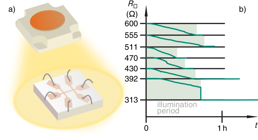
After characterizing the light source, we describe in the rest of this letter our main experiment sketched in Fig. 2 (a) which is installed in a commercial dilution refrigerator (Oxford Instruments, MX250). The Hall bar structured sample is thermally anchored at a sample stage. The temperature of the sample stage is PID regulated using a resistor chip as heater and can be controlled in the range K. Reaching higher temperatures is difficult without removing the 3He/4He insert from the liquid helium bath. Nevertheless, we managed to heat our sample to about K by running our insert in a special operation mode (see below). In this case the temperature is only weakly controlled. The sheet resistance of the sample is measured with a lock-in technique: An ac current of amplitude nA which is reduced to nA for temperature dependent measurements is sourced to the central strip of the Hall bar structure. The resulting voltage drop over two side terminals is amplified by a home-build amplifier and measured by the lock-in amplifier (Signal Recovery, Model 7265 DSP). The length between the voltage terminals equals 12 times the width of the central strip and . We carefully checked that we stay in the linear regime of the current voltage characteristics which made it necessary to reduce the measurement current close the superconducting transition. Hall resistance is recorded in fields up to T by measuring the voltage across two terminals opposite to each other and supplies us with information on the sheet carrier concentration.
The LED light source is mounted at mm distance from the sample. LED currents of nA µA are supplied by a source/measure unit (Keithley Model 2400) via superconducting leads. Operating the LED at higher power leads to a heat burden of the sample stage. In principle could replace the current sourced to in the PID regulation circuit. For the experiments described here we use for temperature control and always stabilize the stage at mK before slowly turning on . The PID regulation reacts to increasing by reducing the current sourced to keeping almost constant (mK). At µA the current through is set to zero by the PID circuitry and heating is solely due to the dissipation of the LED.
Constant does not automatically guarantee a constant temperature of the 2DEG at the LAO/STO interface of our sample. Because of the positive temperature coefficient of at mK, an increase of temperature of the 2DEG as response to irradiation would result in an increase of . In the contrary, light exposure at constant leads to a decrease of . It alters the resistive state of our sample and this alteration cannot be attributed to heating. Examples are given in in Fig. 2 (b). Within the green marked period the sample was illuminated by setting to values between and µA. During illumination decreases as a function of time. As soon as we turn off , stabilizes at its reduced, momentary value. As long as the LED remains switched off and K, is a function of magnetic field and temperature only and does not change over time. Initially, was found to be . Subsequently we altered the resistive state of our sample in steps of about . In Fig. 3 (a) where is displayed as a function of the radiant exposure , this first series is represented by red symbols. The abscissa in this figure is deduced from with the help of the LED calibration presented earlier and corresponds to the total radiant energy per unit area irradiated to the sample by the LED in the short wavelength part of the spectrum. Most likely only high energetic photons are responsible for the persistent conductance effect.Yazdi-Rizi et al. (2017) However, we do not have further evidence for this statement and additional experiments with monochromatic LEDs are required for a proof. The total radiant exposure over all wavelength is 70% larger.
Light exposure leads to persistent reduction of . However, the resistance change can be reverted by heating the sample to K. The rate of resistance increase depends in this case on temperature and speeds up considerable above K. Unfortunately it is almost impossible to regulate temperatures in the regime K in our dilution fridge. While we could reach temperatures of the order K K by thermally isolating111This is done by pumping out the 3He/4He-mixture. An absorption pump at the condenser is still kept at K to maintain good isolation from the 4He bath. This, actually, limits the maximal sample temperature we can reach by heating the mixing chamber. and heating the mixing chamber this temperature is only weakly controlled. Nevertheless, we could convince ourselves, that measured after cooling the sample down again after heat treatment depends strongly on the peak temperature reached during the procedure and only weakly on the time period it lasts. The minimal resistance we could achieve by irradiation is in this respect related to the temperature mK at which it is measured and lower resistive states might in principle be reached by irradiation at lower temperatures but relax back to if the sample is heated to mK.
By controlled heating we are able to increase in small steps. Again, at low temperature and while the LED is switched off, is a function of magnetic field and temperature only and is absolutely stable over time. By heating the sample to K we could reach resistance states with even slightly higher than the initial value of . Subsequently we lowered the resistance again by utilizing the LED. This second run is shown as green symbols in Fig. 3 (a) giving consistent results. Analyzing the dependence of gives the empirical results shown as black lines in Fig. 3 (a). The experimental data are well described by
with different initial resistance values (, ) and slopes (dB, dB) at lower and higher dose, respectively.
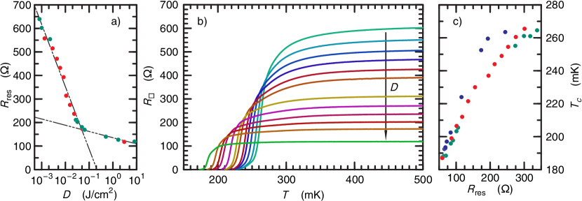
In Fig. 3 (b) we present in the different persistent resistance states of the first light induced reduction series (corresponding to the red symbols in Fig. 3 (a)). During this measurements . The curves in Fig. 3 (b) display superconductivity at low temperatures with a transition temperature which shifts downwards with decreasing . This effect is summarized in Fig. 3 (c) where was estimated as the temperature where . In the initial sequence of resistance reduction by illumination decreased monotonically from mK down to mK. The blue symbols represent the findings when recovers due to controlled heating. could be reached easily by heating the sample to K. In this state fully recovers to mK. We then kept the sample for an extended period of several days at K and could increase even further (). However, this had only a minor effect on . The final illumination sequence with falling is shown as green symbols and shows the reproducibility of our finding.
The observed reduction of with decreasing is typical for the so called over-doped regime and indeed taking the resistance range of our experiment () into account this finding is in accord with published dataCaviglia et al. (2008); Gariglio, Gabay, and Triscone (2016) on field effect tuned resistivities. Our Hall resistivity measurements show a zero field slope (T) which is almost independent of in accordance with data presented in Ref. Joshua et al., 2012. Within the limited field range of our magnet (T) we only see slight nonlinearities at larger fields which get more pronounced as is lowered. This trend has already been reported previously for LAO/STO in the overdoped regime.
For now, the microscopic mechanism of light induced changes is absolutely unclear. Findings by other authorsYazdi-Rizi et al. (2017) differ in subtle details. We completely revert the photo-induced transport changes at comperatively low temperatures (K) while in Ref. Yazdi-Rizi et al., 2017 a crossing of the antiferro-distortive transition of STO at K seems to be necessary to revert persistence in photo-conductance. The difference might route in a smaller photon energy in our case. The LED radiates at eV, which is of the order but considerable smaller than the band gap of STO (eV). Other experiments on persistent photo-conductance use UV light above the gap energy.
In summary, we present a setup to tune the transport behavior of STO-based interfaces at low temperatures with light. The radiant intensity of a LED was calibrated at K as a function of current and utilized as the light source below 1 K. Adjusting the radiant energy we were able to tune the residual sheet resistance at 500 mK, while simultaneously changing the superconducting transition temperature . We reported a monotonous behavior of vs for different resitive states. To reverse the altered state we used heat treatment up to 12 K. Using visible light at low temperatures we are introducing a new nonvolatile tuning parameter on the superconductivity of the STO-based interfaces.
This paper was supported by the Deutsche Forschungsgemeinschaft (Grant SCHA 658/2-1 and FU 457/2-1). We thank K. Grube for fruitful discussion.
References
- Ohtomo and Hwang (2004) A. Ohtomo and H. Y. Hwang, “A high-mobility electron gas at the / heterointerface,” Nature 427, 423–426 (2004).
- Seo et al. (2007) S. S. A. Seo, W. S. Choi, H. N. Lee, L. Yu, K. W. Kim, C. Bernhard, and T. W. Noh, “Optical study of the free-carrier response of / superlattices,” Phys. Rev. Lett. 99, 266801 (2007).
- Perna et al. (2010) P. Perna, D. Maccariello, M. Radovic, U. Scotti di Uccio, I. Pallecchi, M. Codda, D. Marré, C. Cantoni, J. Gazquez, M. Varela, S. J. Pennycook, and F. M. Granozio, “Conducting interfaces between band insulating oxides: The / heterostructure,” Applied Physics Letters 97, 152111 (2010), https://doi.org/10.1063/1.3496440 .
- Moetakef et al. (2011) P. Moetakef, T. A. Cain, D. G. Ouellette, J. Y. Zhang, D. O. Klenov, A. Janotti, C. G. Van de Walle, S. Rajan, S. J. Allen, and S. Stemmer, “Electrostatic carrier doping of / interfaces,” Applied Physics Letters 99, 232116 (2011), https://doi.org/10.1063/1.3669402 .
- Li, Wang, and Dai (2011) D. F. Li, Y. Wang, and J. Y. Dai, “Tunable electronic transport properties of / polar heterointerface,” Applied Physics Letters 98, 122108 (2011), https://doi.org/10.1063/1.3570694 .
- Lee et al. (2012) S. W. Lee, Y. Liu, J. Heo, and R. G. Gordon, “Creation and control of two-dimensional electron gas using Al-based amorphous oxides/ heterostructures grown by atomic layer deposition,” Nano Letters 12, 4775–4783 (2012), https://doi.org/10.1021/nl302214x .
- He et al. (2012) C. He, T. D. Sanders, M. T. Gray, F. J. Wong, V. V. Mehta, and Y. Suzuki, “Metal-insulator transitions in epitaxial and films,” Phys. Rev. B 86, 081401 (2012).
- Annadi et al. (2012) A. Annadi, A. Putra, Z. Q. Liu, X. Wang, K. Gopinadhan, Z. Huang, S. Dhar, T. Venkatesan, and Ariando, “Electronic correlation and strain effects at the interfaces between polar and nonpolar complex oxides,” Phys. Rev. B 86, 085450 (2012).
- Li et al. (2013) C. Li, Q. Xu, Z. Wen, S. Zhang, A. Li, and D. Wu, “The metallic interface between insulating and perovskites,” Applied Physics Letters 103, 201602 (2013), https://doi.org/10.1063/1.4830042 .
- Chen et al. (2013) Y. Z. Chen, N. Bovet, F. Trier, D. V. Christensen, F. M. Qu, N. H. Andersen, T. Kasama, W. Zhang, R. Giraud, J. Dufouleur, T. S. Jespersen, J. R. Sun, A. Smith, J. Nygård, L. Lu, B. Büchner, B. G. Shen, S. Linderoth, and N. Pryds, “A high-mobility two-dimensional electron gas at the spinel/perovskite interface of /,” Nature Communications 4, 1371 (2013).
- Xu et al. (2014) P. Xu, D. Phelan, J. Seok Jeong, K. Andre Mkhoyan, and B. Jalan, “Stoichiometry-driven metal-to-insulator transition in / heterostructures,” Applied Physics Letters 104, 082109 (2014), https://doi.org/10.1063/1.4866867 .
- Zubko et al. (2011) P. Zubko, S. Gariglio, M. Gabay, P. Ghosez, and J.-M. Triscone, “Interface physics in complex oxide heterostructures,” Annual Review of Condensed Matter Physics 2, 141–165 (2011), https://doi.org/10.1146/annurev-conmatphys-062910-140445 .
- Huijben et al. (2006) M. Huijben, G. Rijnders, D. H. A. Blank, S. Bals, S. V. Aert, J. Verbeeck, G. V. Tendeloo, A. Brinkman, and H. Hilgenkamp, “Electronically coupled complementary interfaces between perovskite band insulators,” Nature Materials 5, 556–560 (2006).
- Lei et al. (2014) Y. Lei, Y. Li, Y. Z. Chen, Y. W. Xie, Y. S. Chen, S. H. Wang, J. Wang, B. G. Shen, N. Pryds, H. Y. Hwang, and J. R. Sun, “Visible-light-enhanced gating effect at the / interface,” Nature Communications 5, 5554 (2014).
- Li et al. (2015) Y. Li, Y. Lei, B. G. Shen, and J. R. Sun, “Visible-light-accelerated oxygen vacancy migration in strontium titanate,” Scientific Reports 5, 14576 (2015).
- Tebano et al. (2012) A. Tebano, E. Fabbri, D. Pergolesi, G. Balestrino, and E. Traversa, “Room-temperature giant persistent photoconductivity in / heterostructures,” ACS Nano 6, 1278–1283 (2012), https://doi.org/10.1021/nn203991q .
- Yang et al. (2017) Z. Yang, Y. Chen, H. Zhang, H. Huang, S. Wang, S. Wang, B. Shen, and J. Sun, “Joint effect of gate bias and light illumination on metallic / interface,” Applied Physics Letters 111, 231602 (2017), https://doi.org/10.1063/1.5009790 .
- Cheng et al. (2017) L. Cheng, L. Wei, H. Liang, Y. Yan, G. Cheng, M. Lv, T. Lin, T. Kang, G. Yu, J. Chu, Z. Zhang, and C. Zeng, “Optical manipulation of rashba spin–orbit coupling at -based oxide interfaces,” Nano Letters 17, 6534–6539 (2017), https://doi.org/10.1021/acs.nanolett.7b02128 .
- Yazdi-Rizi et al. (2017) M. Yazdi-Rizi, P. Marsik, B. P. P. Mallett, K. Sen, A. Cerreta, A. Dubroka, M. Scigaj, F. Sánchez, G. Herranz, and C. Bernhard, “Infrared ellipsometry study of photogenerated charge carriers at the (001) and (110) surfaces of crystals and at the interface of the corresponding / heterostructures,” Phys. Rev. B 95, 195107 (2017).
- Reyren et al. (2007) N. Reyren, S. Thiel, A. D. Caviglia, L. F. Kourkoutis, G. Hammerl, C. Richter, C. W. Schneider, T. Kopp, A.-S. Rüetschi, D. Jaccard, M. Gabay, D. A. Muller, J.-M. Triscone, and J. Mannhart, “Superconducting interfaces between insulating oxides,” Science 317, 1196–1199 (2007), https://science.sciencemag.org/content/317/5842/1196.full.pdf .
- Biscaras et al. (2010) J. Biscaras, N. Bergeal, A. Kushwaha, T. Wolf, A. Rastogi, R. C. Budhani, and J. Lesueur, “Two-dimensional superconductivity at a mott insulator/band insulator interface /,” Nature Communications 1, 89 (2010).
- Fuchs et al. (2014) D. Fuchs, R. Schäfer, A. Sleem, R. Schneider, R. Thelen, and H. von Löhneysen, “Two-dimensional superconductivity between and amorphous ,” Applied Physics Letters 105, 092602 (2014), https://doi.org/10.1063/1.4895120 .
- Thiel et al. (2006) S. Thiel, G. Hammerl, A. Schmehl, C. W. Schneider, and J. Mannhart, “Tunable quasi-two-dimensional electron gases in oxide heterostructures,” Science 313, 1942–1945 (2006), https://science.sciencemag.org/content/313/5795/1942.full.pdf .
- Caviglia et al. (2008) A. D. Caviglia, S. Gariglio, N. Reyren, D. Jaccard, T. Schneider, M. Gabay, S. Thiel, G. Hammerl, J. Mannhart, and J.-M. Triscone, “Electric field control of the / interface ground state,” Nature 456, 624–627 (2008).
- Gariglio, Gabay, and Triscone (2016) S. Gariglio, M. Gabay, and J.-M. Triscone, “Research update: Conductivity and beyond at the / interface,” APL Materials 4, 060701 (2016), https://doi.org/10.1063/1.4953822 .
- Fuchs et al. (2015) D. Fuchs, A. Sleem, R. Schäfer, A. G. Zaitsev, M. Meffert, D. Gerthsen, R. Schneider, and H. v. Löhneysen, “Incipient localization of charge carriers in the two-dimensional electron system in / under hydrostatic pressure,” Phys. Rev. B 92, 155313 (2015).
- Fuchs et al. (2017) D. Fuchs, K. Wolff, R. Schäfer, R. Thelen, M. Le Tacon, and R. Schneider, “Patterning of two-dimensional electron systems in based heterostructures using a template,” AIP Advances 7, 056410 (2017), https://doi.org/10.1063/1.4973696 .
- Wolff et al. (2018) K. Wolff, R. Eder, R. Schäfer, R. Schneider, and D. Fuchs, “Anisotropic electronic transport and rashba effect of the two-dimensional electron system in (110) -based heterostructures,” Phys. Rev. B 98, 125122 (2018).
- osr (2010) Golden DRAGON Plus, Osram Opto Semiconductors GmbH (2010).
- Note (1) This is done by pumping out the 3He/4He-mixture. An absorption pump at the condenser is still kept at K to maintain good isolation from the 4He bath. This, actually, limits the maximal sample temperature we can reach by heating the mixing chamber.
- Joshua et al. (2012) A. Joshua, S. Pecker, J. Ruhman, E. Altman, and S. Ilani, “A universal critical density underlying the physics of electrons at the / interface,” Nature Communications 3, 1129 (2012).