Spin-valley system in a gated MoS2-monolayer quantum dot
Abstract
The aim of presented research is to design a nanodevice based on a gate-defined quantum dot within a MoS2 monolayer in which we confine a single electron. By applying control voltages to the device gates we modulate the confinement potential and force intervalley transitions. The present Rashba spin-orbit coupling additionally allows for spin operations. Moreover, both effects enable the spin-valley SWAP. The device structure is modeled realistically, taking into account feasible dot-forming potential and electric field that controls the Rasha coupling. Therefore, by performing reliable numerical simulations, we show how by electrically controlling the state of the electron in the device, we can obtain single- and two-qubit gates in a spin-valley two-qubit system. Through simulations we investigate possibility of implementation of two qubits locally, based on single electron, with an intriguing feature that two-qubit gates are easier to realize than single ones.
pacs:
73.63.Kv, 73.22.-f, 85.35.Gv, 03.67.LxI Introduction
Two-dimensional crystals consisting of single layers of atoms are modern materials that can be used for implementation of quantum computation. 2D monolayers of transition metal dichalcogenides (TMDCs), e.g. MoS2, seem to be better candidates than graphene because of their wide band gaps and strong electrically induced spin-orbit coupling of the Rashba typeWang et al. (2012); Kormányos et al. (2014a). By considering the valley degree of freedom of an electron together with its spin we extend our ability to define a qubit into: spin, valleyPawłowski et al. (2018) and hybrid spin-valley qubitSzéchenyi et al. (2018). However, the most interesting is the definition based on spin and valley of a single electron as a two-qubit systemRohling and Burkard (2012); Wu et al. (2016).
The area of application of monolayer materials for construction of electronic nanodevices is currently under strong development Papadopoulos et al. (2019); Shang et al. (2019); Paul et al. (2019); Wang et al. (2012); Pisoni et al. (2019); Ghiasi et al. (2019); Huang et al. (2018). Methods for building devices based on gated TMDC monolayers or nanotubes become increasingly advancedKim et al. (2019a); Sahoo et al. (2019); Wang et al. (2018); Kim et al. (2019b); Reinhardt et al. (2019), opening the possibility of utilizing the spin and valley index of electrons controlled therein. In particular, it is shown by recent results with electrostatic quantum dots (QDs) with a gated MoS2-nanoribbon-QD measured by a single electron transportKotekar-Patil et al. (2019); Zhang et al. (2017), or tunable TMDC spintronic devices, where spin or valley polarized currents emerge in TMDC monolayer proximitized by nearby ferromagneticCortés et al. (2019); Zollner and Fabian (2019); Yuan et al. (2018); Li et al. (2014); Majidi and Asgari (2014). Transistor structures with TMDC monolayer forming active area in tunnel FETs are being developedIlatikhameneh et al. (2015), also with vertical TMDCs heterostructures Georgiou et al. (2012); Wu et al. (2019). The more intriguing lateral, in-plane TMDCs heterojunctions are also constructed, enabling interesting 1D physics at interfacesÁvalos-Ovando et al. (2019), or leading to improved FETs switching characteristics Choukroun et al. (2018); Marian et al. (2017); Iannaccone et al. (2018).
Inspired by this, we examined the possibility of realization of a nanodevice based on a MoS2 monolayer, capable of creating a two-qubit system defined on spin and valley degrees of freedom of a confined electron. For this purpose, we have built a realistic model of the nanodevice and perform numerical simulations that prove its capabilities. Thanks to the use of appropriately modulated local control voltages, the system is all-electrically controlled and does not require using photons or external microwaves, thus significantly improving its scalability.
II Model
In this section we will go through the device model. The potential in the entire nanodevice, controlled by the gate voltages, is calculated by solving the Poisson equation, while the electron states in the flake are described with the tight-binding formalism. Let’s start with the nanostructure overview.
II.1 Device structure
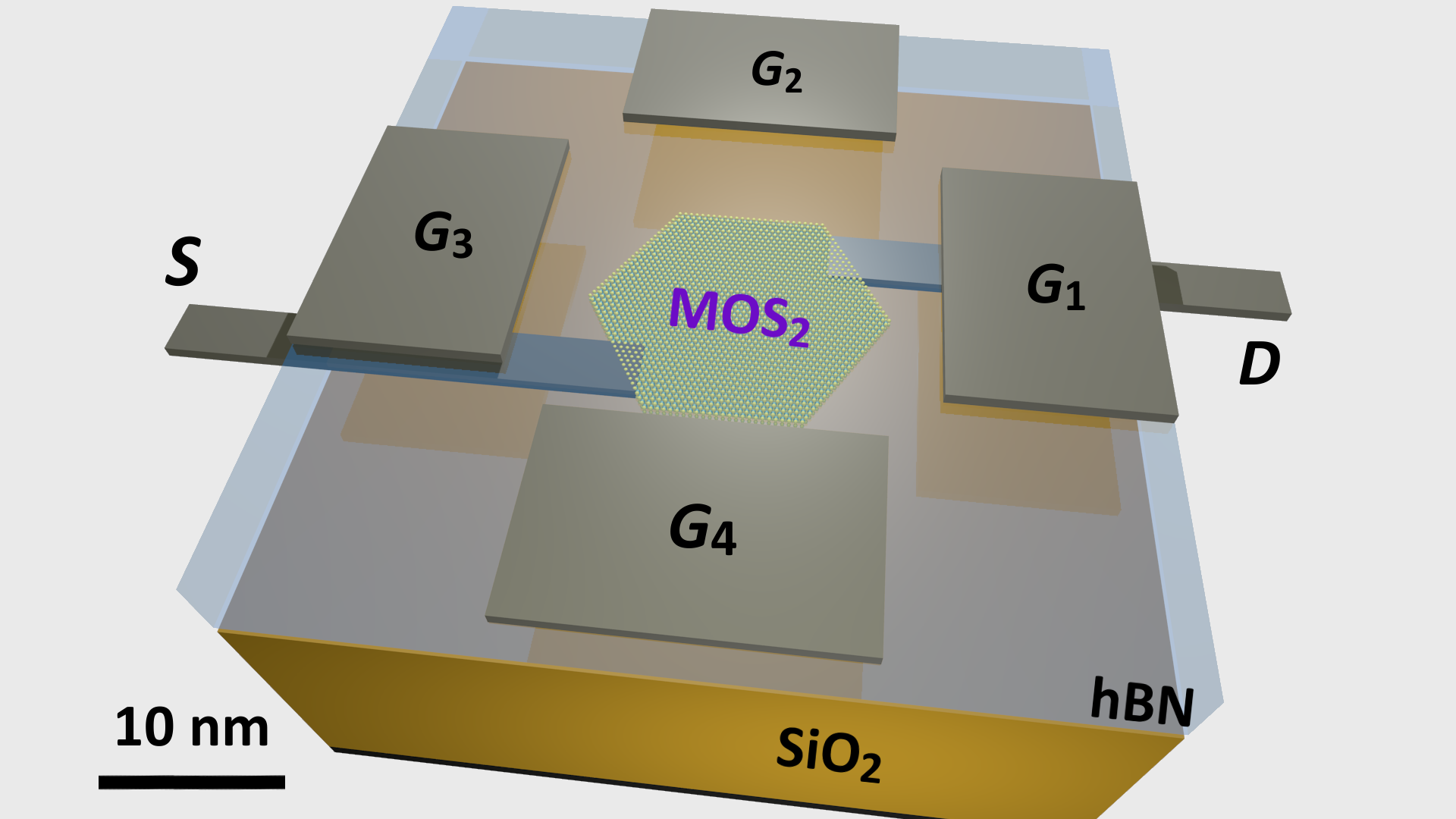
The proposed nanodevice structure is presented in Fig. 1. On a strongly doped silicon substrate we place a 20-nm-thick layer of SiO2. Then we place two electrodes which serve as a source () and a drain (). Directly on them we deposit a MoS2-monolayer (hexagonally shaped) flake of 16-nm-diameter. The monolayer is then covered with a -nm thick insulating layer of hexagonal boron nitride (hBN) with a large bandgapLaturia et al. (2018), forming a tunnel barrier. Finally on top of the sandwiched structure we lay down four 15-nm-wide control gates (), placed symmetrically around the central square-like gap of size nm. The gate layout presented here is quite similar to the one proposed by us recentlyPawłowski et al. (2018), but with a larger nm clearance between opposite gates, which may ease their deposition.
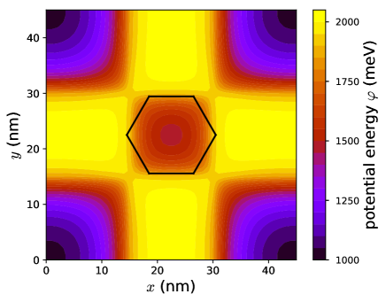
Source, drain and the gates layout are clearly presented in Fig. 1. Voltages applied to these gates (relative to the substrate) are used to create confinement in the flake. To calculate realistic electrostatic potential we solve the Poisson equation taking into account voltages applied to control gates and to the highly doped substrate , together with space-dependent permittivity of different materials in the devicePawłowski et al. (2018, 2016). Resulting potential in the area between SiO2 and hBN layers, where the flake is sandwiched, is presented in Fig. 2.
We deplete the electron gas until a single electron remains in the formed dot confinement potential.
II.2 Monolayer model
The monolayer flake is made of molybdenum disulfide.
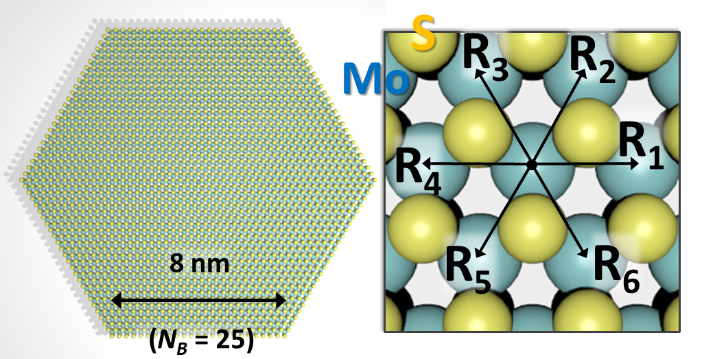
MoS2 monolayers are successfully described by several tight-binding (TB) models, with different numbers of orbitals used, including nearest or next-nearest neighbors. SevenRostami et al. (2013) or elevenRidolfi et al. (2015); Cappelluti et al. (2013); Fang et al. (2015) Mo and S orbitals construct TB basis to reproduce low-energy physics in the entire Brillouin zone, also near the -point. Although the simpler three-band (including three Mo orbitals) TB modelLiu et al. (2013) fails around the -point, it correctly represents the orbital composition around the K point near the (both conduction and valence) band edges, where the Bloch states mainly consist of Mo orbitalsKadantsev and Hawrylak (2012). Thus it is good enough to deal with low energy states near the band minimum. However when considering perpendicular electric field, crucial for the Rashba coupling, we have to include also S orbitals localized above and below Mo plane in the MoS2 structure (see Fig. 3). For calculating Rashba coupling we will utilize 11-band model with three orbitals for each S atom in dimer.Ridolfi et al. (2015)
Consequently, we have described the monolayer structure using three Mo orbitals: , , , and the nearest-neighbors hoppingsLiu et al. (2013):
| (1) |
The potential energy of the electrostatic confinement at the -th lattice site: together with the on-site energies enter the on-diagonal matrix elements ( numbers the orbitals).
The off-diagonal electron hopping element from the Mo orbital localized in the -th lattice site to the orbital localized in the -th site is denoted by . It depends on the hopping direction (between neighbor pair) described by the nearest neighbor vectors for the molybdenum (Mo) lattice, which are defined as in Fig. 3. They form two non-equivalent families: , , and , , with the nearest sulphur (S) neighbor on the left or right side, as shown in Fig. 3. This symmetry constraint reflects on the reciprocal lattice where in the corners of the first (hexagonal) Brillouin zone, the K points form two non-equivalent families: and .
II.3 Rashba coupling
Electric field perpendicular to the monolayer surface breaks the reflection symmetry and modifies the on-site energies of atoms in three MoS2 sublayers. This leads to externally, electrically controlled spin-orbit interaction (SOI) of the Rashba type. The Rashba coupling can be also introduced to layered TMDCs by a structure asymmetry from ferromagnetic substrate leading to the proximity effect Cortés et al. (2019).
The idea to calculate the electrically induced Rashba spin-orbit coupling strength is to take the tight-binding model with atomic spin-orbit coupling (introduced by in Eq. II.2) including also orbitals of the sulfur top and bottom sublayers to which we apply on-site potentials and Ochoa and Roldán (2013); Rostami et al. (2013); Petersen and Hedegård (2000); Konschuh et al. (2010). The difference between them results from external electric field: , . While nm is the monolayer thickness (sulfur sublayers distance).
Given such extended tigh-binding model (we take 11-orbital model of Ridolfi et al. [Ridolfi et al., 2015]), we perform downfolding, using the Löwdin partitioning technique, to our Mo-orbitals model and obtain the Rashba coupling within this 3-band base. Further details of the calculation are attached in the Appendix. Resulting coupling matrix elements are proportional to external electric field: , with the explicit form
| (2) |
The tight-binding Rashba HamiltonianKlinovaja and Loss (2013a, b); Konschuh et al. (2010); Ezawa (2014); Kane and Mele (2005) (in Eq. II.2) with characteristic spin- and orientation-dependent hopping between two nearest neighbor bonds is:
| (3) |
with the Pauli-matrices vector , and the (unit) versor pointing along the bond connecting sites and . An obvious property ensures hermiticity. The expanded hopping expression is , where , , and with the above defined .
II.4 External magnetic field
To include electron interaction with a perpendicular magnetic field in the monolayer model, we should add to the Hamiltonian a standard Zeeman term (in Eq. II.2):
| (4) |
with a magnetic field . For we arrive at the standard Zeeman energy .
To address also orbital effects related to magnetic field we apply the so-called Peierls substitutionHofstadter (1976). We multiply the hopping matrix, by the additional factor in the Hamiltonian (II.2). Now the vector potential enters Eq. (II.2) via the Peierls phase , calculated as the path integral between neighbor nodes:
| (5) |
is a vector potential induced by the field. We use the Landau gauge, with the vector potential for the perpendicular magnetic field . This leads to the phase:
| (6) |
The most important result of applying a magnetic field is a splitting introduced between levels with opposite spin and valley index. Interestingly there are two types of Zeeman splittings: standard, spin type, and Zeeman valley splitting, both presented in Fig. 6 in Section IV. Each of them possesses other Landé factor. This will enable us to separately address each transition between four basis states in the spin-valley two-qubit space.
III Calculation method
Let’s have a look at the stationary and time-dependent calculation methodology. Firstly, we solve the eigenproblem for the stationary Hamiltonian (II.2): , and obtain eigenstates. For our hexagonal flake of size we have giving eigenstates. For the Hamiltonian matrix eigenproblem we utilize the fast and efficient FEAST routinePolizzi (2009). The obtained eigenstates are represented by 6-dimensional vectors , with and . They belong to te state space , with the spin and the 3-dimensional Mo-orbitals space. To identify them, at first we need an electron density calculated as to determine if given state is localized at the flake edge forming the so-called edge state, or is confined within the quantum-dot. Secondly, we need to identify the state quantum numbers—valley and spin indices. To do this we utilize similar formulas as in Eqs. (12) and (13), here adapted to a stationary state .
During the time-dependent calculations we will be working in the previously found eigenstates base. Therefore the full time-dependent wave function is represented as a linear combination of basis states :
| (7) |
together with time-dependent amplitudes and phase factors of the corresponding eigenvalues . We assume a basis of lowest eigenstates from the conduction band (represented by yellow bullets in the lower inset in Fig. 5). The time evolution is governed by the time-dependent Schrödinger equation:
| (8) |
with the time-dependent Hamiltonian being a sum of the stationary part (Eq. II.2) and a time-dependent contribution to both the potential energy and the Rashba coupling:
| (9) |
The full time-dependent potential energy contains variable part , generated by modulation of the gate voltages. Whole is calculated as , with the potential obtained by solving the Poisson equation for the variable density at every time step. Note that the charge density originates from the actual wave-function, thus the Schrödinger and Poisson equations are solved in a self-consistent way. Similarly, the time-dependent part of the Rashba coupling is induced by the variable part of the electric field: . That is, induces (3), while enters in (9) with the same formula.
Insertion of (7) to the Schrödinger equation (8) gives a system of equations for time-derivatives of the expansion coefficients at subsequent moments of time:
| (10) |
The actual matrix elements need to be calculated at every time step due to changes in the potential and the electric field. Then, by using it, we solve the system (10) iteratively using a predictor-corrector method, with explicit “leapfrog” and implicit Crank-Nicolson scheme, obtaining the next time step of the system evolution.
For the electron wave function we calculate the Fourier transform:
| (11) |
on the flake surface area , with 2D-wave vector . The Fourier transform naturally has periodic structure in the reciprocal space, therefore we can limit the -area to : , encompassing the (first) Brillouin Zone (BZ). Knowing we can calculate density in the reciprocal space expressed as: . The -density calculated for the state from Fig. 5 is presented in Fig. 10(). We also mark the BZ along with points of high symmetry: in the center, two types of () at the corners of the hexagonal zone and on the edges of the hexagon. The coordinates of the high-symmetry points are: , one of and one of , with the lattice constant nm. We can clearly see in Fig. 10() that density peaks are localized in the neighborhood of the points (while not next to ), confirming that in the state exactly valley is occupied.
Now, the valley index is calculated as:
| (12) |
on the reciprocal space area defined as two opposite sectors (within area) encompassing exactly one point and one point, i.e. , with azimuthal angle . Because () point in has coordinates (), the valley index . represents the valley, whereas the valley. For example the state is thus represented by ket.
The electron spin value is calculated as the expectation value of the Pauli -matrix :
| (13) |
also integrated on the flake area for the actual wave vector . Operation means that during the spin calculations we trace out over the orbitals subspace.
IV Electrostatic quantum dot
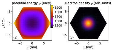
By applying voltages mV to all of the gates we form the QD potential energy in the flake area, presented in Fig. 4(a). Calculated electronic eigenstates of the Hamiltonian (II.2) for the entire flake lattice, forms a ladder in Fig. 5 representing subsequent eigenstates . The bullets color is used to mark the dot occupation, namely the brighter the color is, the electron is more localized in the flake center. E.g. the yellow states are strongly confined, while black color marks the edge states with density localized on the flake border. These states are inaccessible to the electron confined in the QD, forming a forbidden energy range, namely, a bandgap. The bandgap divides the QD eigenstates into conduction and valence bands. Lets now zoom into CB minimum. The states therein are presented in insets from Fig. 5.
The first four states form two doublets and , spin-orbit split (see the upper inset in Fig. 5). Their electron density is presented in Fig. 4(b).
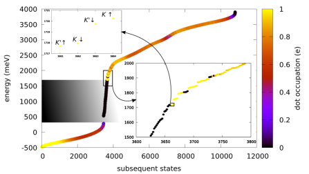
It turns out, that (states from) both the bottom of the conduction band and the top of the valence band are located at the points and (we have a direct band gap here), not at the point. These bands form two non-equivalent valleys and which can be occupied by qubit carriers. Subspace spanned by the first four states consists of exactly one valley and one spin two-level system, forming together a 4-dimensional Hilbert space of spin-valley two-qubit states .
IV.1 Two-qubit subspace
If we add an external magnetic field, degeneracy in both pairs is lifted, as presented in Fig. 6 for T.
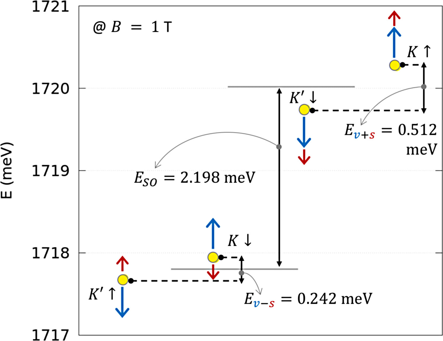
Calculated splitting, here for T (for T resulting factors are the same), between first pair: (split down) and (split up) is eV, which is in agreement with differences eV between opposite spin states (with different valleys) in the conduction band minimum for a larger dot [Dias et al., 2016]. The difference of eV leads to . For the second pair (split down) and (split up) we have eV, thus . Therefore, obtained effective valley and spin g-factors are: , similar to DFT calculations giving the value 7.14 [Kormányos et al., 2014a, and errata: Kormányos et al., 2014b]. While the spin splitting factor , with agreement with the DFT calculations [Kormányos et al., 2014a] and experimental result [Marinov et al., 2017], both giving value about .
If we now take into account both spin and valley splitting, it turns out that the higher states pair is more split than the lower one, as presented in Fig. 6. This results from emergence of additional valley Zeeman splitting, for which levels bend upwards and for downwards (blue arrows). Similarly, spin-down level bends down, while spin-up bends up (red arrows). Therefore, for the higher levels pair the splittings will add, while for the lower one they will subtract. Thanks to such a form of level splittings, all of the transitions between them (6 in total) can be separately addressed.
IV.2 Intervalley coupling
Let’s now examine the intervalley coupling strength and its origin. The doubled intervalley coupling can be calculated from the difference between the ground state and the 1st excited state in CB with no spin-orbit interactionLiu et al. (2014). Further, we assume that the intervalley coupling is: , with a modulation amplitude .
The structure of electronic states confined within a nanoflake and mostly presence of edge states, that cross the gap, depends on the flake edge typeBrey and Fertig (2006); Zarenia et al. (2011); Szafran et al. (2018a). Zigzag edges do not mix valleys, but supports edge states. On the other hand, gap states are missing for an armchair edge type, which mixes valleys and induces transitions in graphene-like structuresSzafran et al. (2018b). Same edge-dependent valley mixing was proven for MoS2 nanoribbonsRostami et al. (2016). Here, to skip the edge influence, we take a flake with a zigzag edge, and induce confinement strong enough to decouple the electron from the flake edge.
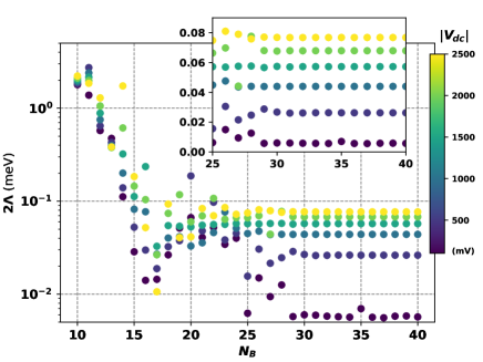
To check completely the edge influence on the intervalley mixing, we calculate as a function of the flake size and the confinement depth, controlled by . The results with no confinement are presented in Fig. 7, by dark-blue bullets. While there is significant coupling for very small flakes with , it suddenly decreases with the flake size, reaching two orders smaller value for . Then the coupling slightly increase, but for larger flakes with it generally does not exceed several eV. However if we add the confinement potential by applying , the intervalley coupling increases with the potential depth, which is clearly visible for . Subsequent voltage values, marked by the brighter bullets, are = mV. It turns out that the approximate relation between the coupling and the applied voltage in this range of the flake sizes is . It is similar to the relation between eigenenergies and potential of a harmonic oscillator. Now the coupling is purely confinement-dependent and does not depend on the flake size. This is because the confined electron is decoupled from the edge and its valley mixing is controlled electrically via the confinement potential.
A 10-nm-scale lithographic process required in in Fig. 1 can be difficult to achieve. Our calculations show that scaling up the structure (with preserved gate voltages) will decrease the intervalley coupling amplitude as , where is the gate width. This means that after magnifying gates layout by an order of magnitude the coupling still keeps reasonable values. However, such scaling proportionally extends the intervalley transition time.
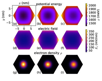
V Spin-valley two qubit system
Let’s now switch to the time-dependent calculations and examine the process of inducing transitions within the defined spin-valley subspace. By applying additional oscillating voltage to the single control gate : , mV together with mV, we modulate the confinement potential in a way that the dot minimum oscillates back and forth in the -direction. The potential energy landscape at oscillations start, i.e. at , is presented in Fig. 8(b). While its form at the maximum left and right displacement from the center position, e.g. at and , is presented in Figs. 8(a) and 8(c) respectively. Additionally to inducing oscillatory movement of the dot position, the potential shape is modulated and becomes narrower at the maximum shift to the left—see Fig. 8(a), while shallower at the maximum right—Fig. 8(c). This enforces oscillatory squeezing of the electron state density, as seen in Fig. 8(g-i).
V.1 Spin and valley transitions
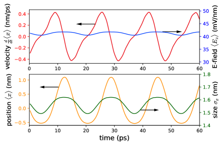
The confinement potential modulation introduces two effects to the system. Firstly, the voltage modulation moves the electron confined in the QD potential in an oscillatory way. The electron position oscillations causes that its momentum also oscillates. The velocity defined as the time derivative of the electron expectation position is presented in Fig. 9 as the red curve, while the electron position as the orange one. Together with the present perpendicular electric field felt by the electron (blue curve in Fig. 9) which induces the Rashba SOI, it creates spin-orbit mediated electron spin resonance transitions. The mean electric field is almost constant during oscillations, which is related to fact that the perpendicular electric field component is mostly uniformly distributed on the flake, as seen in Fig. 8(d-f).
Secondly, oscillatory shallowing of the confinement potential leads to electron packet squeezing, visible as oscillations of the electron packet size in Fig. 9 (green curve) and causes intervalley coupling changes. Resonant modulation of the intervalley coupling generates gradual transitions of the electron between the different valley statesPawłowski et al. (2018).
Subsequent stages of a transition between the different valleys in reciprocal space are presented in Fig. 10.
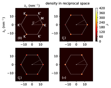
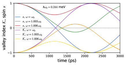
Initially, the electron density in the reciprocal space is localized in the point vicinity within the BZ, as showed in Fig. 10(). The voltage pumping process with the resonant frequency , tuned to the energy spacing between the states and (or and ), leads to a gradual change of occupation to valley, with density flow between valleys visible in the subsequent stages—Fig. 10() and (). After time ps the electron occupies the valley entirely (Fig. 10()) and the intervalley transition is completed. The whole process is presented in Fig. 12, where the green curve represents the valley index evolution during the entire transition.
Besides inter- spin and valley transitions we can simultaneously obtain spin and valley manipulation leading to inter spin-valley transitions or simply the spin-valley SWAP. Similarly here transitions are resonant and we need to tune the modulation frequency to the energy spacing between and (or and ). During voltage oscillations both the Rashba SOI mediated spin transitions and the intervalley coupling modulation effects are enabled, thus allowing for simultaneous spin and valley flipping. Both effect are needed: turning off the Rashba SOI, by setting , turns off the spin-valley SWAP. Simulation results are presented in Fig. 11 with the resonance frequency meV and the driving voltage mV. We observe here simultaneous spin (blue curve) and valley index (violet curve) flips. These transitions are obviously of the Rabi oscillations type. If we diverge from the resonance, the maximum (minimum) value of the valley (spin) index falls down rapidly, entering the region of incomplete transitions. In Fig. 11, green and orange (red and yellow) curves pair present spin and valley index courses for a driving frequency () beyond the resonance.
In opposite to spin-valley SWAP, the intervalley transitions are not mediated by the spin-orbit coupling, and are unaffected even if we eliminate the electric field in the simulations, simply by setting in (Eq. 3). Moreover, the transition time depends on the amplitude of the intervalley coupling modulation. In Fig. 12(a) are presented transitions between both valleys, starting from valley with the index .
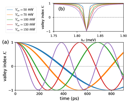
The transition period deceases as the voltage modulation amplitude increases. Indeed, for presented in Fig. 12 amplitude ranges (– mV), oscillations frequency turns out to be approximately proportional to , and thus to the intervalley coupling modulation amplitude (we assume here that for such a small voltage modulation range the intervalley coupling responses linearly—cf. Fig. 7). This is typical for the Rabi oscillations, where near the resonance the Rabi frequency depends linearly on the driving amplitude of the intervalley coupling oscillations. In case of resonance .
If we calculate the minimum value reached by the index for out-of-resonance transitions, we obtain resonance curves presented in Fig. 12(b). The full width at half maximum (FWHM) parameter characterizing resonance curves in case of the Rabi oscillations corresponds to the transition duration. The resonance curve (for driving ) has the form , which gives FWHM equal . This agrees with our calculations. E.g. for the green curve, i.e. mV, transition time (period) is ps, which corresponds to meV and agrees with FWHM equal meV. In comparison, for the violet curve FWHM is just over two times wider than for orange one.
V.2 Two-qubit gates
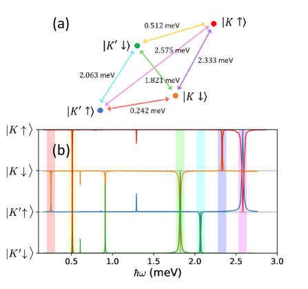
In Fig. 13(a) there are presented four basis states spanning the two-qubit subspace together with all six transitions—each with a different resonant frequency. The voltage modulations induce electron momentum oscillations and intervalley coupling amplitude modulations which enables us to obtain spin operations (blue and violet arrow pair), intervalley transitions (green and purple), or spin-valley swapping (red and yellow). This twofold control of the electron state allows to fully operate within the defined spin-valley two-qubit subspace. Simply, by tuning the modulation frequency we can select and switch-on desired transition.
If we apply a proper magnetic field value (we assume T), the Zeeman splitting together with the spin-orbit induced splitting result in different frequencies among transitions (and allows to separately address each of them). If we now sweep the driving frequency over a range covering all the six transitions, assuming that the system can be initially in four different basis states we observe in Fig. 13(b) all of transitions at their own frequencies. They are highlighted by colors corresponding to colors of the arrows from the scheme in Fig. 13(a). Interestingly we also observe some minor fractional resonances for lower frequencies . Fortunately, they do not overlap with other peaks and transitions are not disturbed by each other. The driving amplitude applied in presented simulations is mV, with an exception for SWAPs where mV.
Let us now translate obtained transitions to the language of qubit operations. Starting from the blue transition from Fig. 13, for pumping at meV, we obtain a spin-flip only if , i.e. valley is occupied. In case of the valley index , we would not observe any operation on spin for such a driving frequency. This means that we get the spin NOT quantum operation controlled by the valley qubit. We denote it simply by . For the violet transition ( meV) we get the opposite CNOT operation with the spin qubit flipped if , denoted by . On the other hand, for the green transition we get complementary operation with the valley index being rotated only if the spin is oriented down. In this case acquiring spin-controlled NOT quantum operation on the valley qubit, analogously denoted as . The purple transition is performed for the opposite, spin-up, thus denoted by . Let us note that the CNOT gates are essential in creating the universal set of quantum gates. Any (multi-qubit) quantum operation can be approximated by a sequence of gates from a set consisting CNOT gate and some single-qubit operationShi (2003), e.g. the gate. If we stop our transitions earlier, we can get various rotation gates. In particular, limiting the operation time in Fig. 14 to of the full valley (spin) flip, i.e. ps ( ps), we realize the rotation acting on the valley (or spin) qubit.
Beside the both CNOT operations with spin or valley serving as the control qubit, while the other one being the target qubit, we can create previously mentioned SWAPs. By taking the red transition we get spin and valley states swapped, i.e. . The complementary operation, induced by the yellow transition, interchanges the two remaining states: . We denote it by . All the mentioned two-qubit operations are represented in the spin-valley two-qubit subspace of states by unitary matrices. Their explicit form can be found in the appendix.
V.3 Single-qubit gates
Two-qubit gates are easy to implement here, because the both qubits are specified on two degrees of freedom of the same particle, thus defined in the same localization. Therefore, coupling between them emerges naturally and two-qubit operations require a single transition between one of the four electron basis states. On the other hand, to obtain a single-qubit gate, acting on a given qubit within such a subspace must be done independently from the other qubit state. It turns out that joining two opposite CNOTs makes the operation on the target qubit independent from the control one. If we perform simultaneously both valley-controlled spin NOTs, i.e. and we arrive at single spin-NOT quantum gate, denoted as , independent from the valley degree. Similarly, for simultaneous and we get valley-NOT, quantum operation.
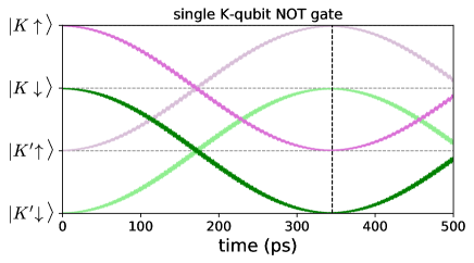
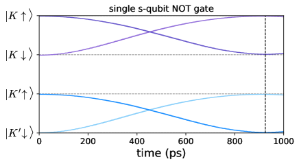
Indeed, to obtain correct operations on spin or valley separately, we need to pump two transitions at the same time. Luckily, it turns out that such twofold transitions are possible, and to do that we need to simultaneously induce oscillations in perpendicular directions, i.e. and , by feeding both and gates. In Fig. 14 there are presented twofold transitions which are composed of two intervalley transitions for both spin orientations making up the valley-NOT operation (top: -qubit NOT gate), and two spin transitions for both valley occupations ( and ) forming -qubit NOT gate (bottom).
The both pumping frequencies and (blue and violet transitions in Fig. 14(bottom)) are very slightly different from these for single separate transitions, e.g. for spin-NOT single-qubit gate they change from to meV for respectively. Whereas the voltage oscillation amplitudes pair should be selected in a way that the both transitions in the pair lasts the same time. The ratio between them should be properly tuned, e.g. for valley-NOT single-qubit gate (green and purple transitions in Fig. 14(top)) for meV respectively.
We see an intriguing feature that local—defined on single electron—two-qubit gates are easier to implement than single-qubit. However, the same single-qubit operations can be obtained a bit easier, simply by performing appropriate CNOTs one by one. Unfortunately, in this simpler approach the operation time is twice as long as for simultaneous twofold transitions. Applying series of operations gives spin-NOT. Similarly, results in valley-NOT. Both relations can be easily verified by multiplying matrices (included in the appendix) representing the particular operations.
V.4 Gate fidelities and qubits readout
In the course of transitions from Figs. 14 or 12 we can notice a minor oscillation structure of frequency related to a single cycle of pumping induced by the voltages oscillations. This can be viewed as a reference frame rotation with frequency in the standard RWA approximationZeuch et al. (2018). However, it should be emphasized that our numerical calculations are strict. These small oscillations affect the qubit operations fidelity. Fortunately, their amplitude decreases as we get closer to the basis states (i.e. poles on the Bloch sphere). Moreover, we can reduce them arbitrarily by decreasing the amplitude of the voltage oscillations. This is at the expense of increasing the number of pumping cycles, and thus increases the operation time.
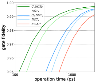
We have performed simulations of the operations for decreasing voltage amplitudes, with simultaneously increasing the gates time. In Fig. 15 there is presented fidelity of various operations as a function of their gate time. One should find an appropriate trade-off between high gate fidelity and low operation time. For example, to obtain an error of the order of 1% (99% fidelity) we find valley-related gates ( and ) duration of about half a nanosecond, and spin-gates about ns. The lowest fidelity is for SWAP operations with a ns optimum for 99%-fidelity. The duration of operations should be much shorter than the coherence time. EstimatedWu et al. (2016) coherence times of electron valley and spin degrees of freedom in MoS2 monolayers, related to the hyperfine interaction decoherence from Mo nuclear spins, are of ns. This is about two orders of magnitude longer than our operation times. The coherence timescale may be slightly overestimatedRivera et al. (2016). However, it scales with the system size as , with the number of nuclear spins covered by the wavefunction density. Thus, coherence time scales up linearly with the system length, and can be extended by increasing the confinement width.
Each full qubit implementation has to comprise initialization and readout. To do this we can utilize the valley- and spin-Pauli blockade, so far observed in carbon nanotubesPei et al. (2012); Laird et al. (2013). The blockade utilizes selection rules, which block electron transport between an adjacent dot with the same valley and spin state. Let us add to the setup a nearby auxiliary dot with an electron in the ground state, i.e. . Assuming that valley and spin are conserved during tunneling, the electron carrying our qubits cannot tunnel to the nearby dot if the electron confined there occupies the same spin and valley stateRohling and Burkard (2012); Osika and Szafran (2017). The electron is blocked in the same state as its neighbor: and both qubits are initialized. However, when we perform operation on valley or spin qubit, the blockade is lifted and the electron can freely enter the nearby dot: with or . In this way, by extending the system with adjacent reference electron, we can perform both—spin or valley qubits readout.
VI Summary
The emerging branch of electronics utilizing the valley degree of freedom, called valleytronics in analogy to spintronics, introduces new intriguing methods for defining qubits. Nanodevices with gated monolayer QDs currently become more reliably fabricated. To advantage this, we investigate the possibility of realization of the spin-valley two-qubit system defined on a single electron, that is confined in a QD, controlled by voltages applied to the device local gates. The proposed nanodevice is modeled after structures that were experimentally realized.
A realistically calculated QD confinement potential and electric field via the Poisson equation together with the exact form of the Rashba coupling within the tight-binding monolayer model, leads to reliable modeling of both the intervalley coupling and the Rashba SOI. We solve the time-dependent Schrödinger equation with such variable confinement, and track the transitions by calculating actual values of the spin and valley index. We also analyze the edge influence on the intervalley coupling with the increasing flake size and confinement depth, concluding that proposed nanodevice will work even if we enlarge the flake and move its edges away.
As a result of the performed simulations, we show feasibility of electrically controlling both the electron spin and valley degrees of freedom, simultaneously. By applying an appropriate magnetic field we get such spin and valley Zeeman splittings, that all of the six possible transitions within the spin-valley subspace can be separately addressed. These transitions are interpreted as a variety of two-qubit gates (i.e. CNOTs and SWAPs), and properly combined, they give single-qubit NOT gates.
Encoding two qubits locally on two degrees of freedom of a single electron reverse difficulty in such a way that two-qubit gates are easer to implement than a single qubit. The latter, however, can be achieved in one go or as two consecutive transitions. By examining the exact course of transitions, we can also estimate fidelity of the implemented gates.
Finally, we remark that to implement fully scalable system, we also need to control interaction between valley (and spin) indexes of nearby electrons in the register. This requires adding additional electrons to the system and research interactions among them.
Acknowledgements.
Author would like to thank Grzegorz Skowron and Paweł Potasz for invaluable discussions. This work has been supported by National Science Centre, under Grant No. 2016/20/S/ST3/00141. This research was supported in part by PL-Grid Infrastructure.Appendix A Rashba coupling parameters
To calculate the Rashba coupling parameter matrix we utilize the 11-band model from [Ridolfi et al., 2015] with five -orbitals in the Mo atom , , , , , and six -orbitals for the S atoms, three for top () and three for bottom () layers: , , . We add the atomic spin-orbit interaction of the form taken from [Roldán et al., 2014; Kośmider et al., 2013] with intrinsic parameters and eV.Kośmider et al. (2013) After calculating appropriate Slater-Koster elements we obtain the full Hamiltonian (together witch spin) [see Appendix B in Ridolfi et al., 2015], with additional onsite potentials for the top/bottom layers, serving as parameters. Now, it can be expressed in an infinite layer-form as a function of the momentum , simply by substituting each hopping .
We calculate numeric value of for different around the CB minimum, i.e. for (or ) and energy level eV. By utilizing the Löwdin partitioning technique Löwdin (1962); Bochevarov and Sherrill (2006); Jin and Song (2011) we downfold it to a reduced Hamiltonian within our 3-band modelLiu et al. (2013); Pavlović and Peeters (2015), used in the simulations. The Schroödinger equation for the full block Hamiltonian is
| (14) |
We perform downfolding by eliminating and arrive at representation where
| (15) |
which is equivalent to (14). Afterwards calculating (15), we finally obtain a numeric value of as a function of . The vector is represented in the basis of orbitals , while .
After the procedure of downfolding to the 3-band model we obtain a matrix representing the Rashba Hamiltonian, indexed by the orbital numbers and , made up of spin blocks. Each of this block has the form , which we write down as
| (16) |
As expected, resulting specific numeric value of each block is proportional to the external electric field . Moreover, it is multiplied by the matrix with phase factors of the form equivalent to in the Hamiltonian from (Eg. 3). The phase depends on the hopping direction, however in our calculations it is undetermined and resulting was disordered.
In this way we obtain the parameter matrix , where
| (17) |
We get the same results for the two remaining points. However, values obtained around point are slightly different
| (18) |
Finally, we take to the model an approximate—average value of the as written down in (2), remembering, however, of slightly different values between valleys. The obtained value corresponds to the Rashba coupling amplitude from [Kormányos et al., 2014a], where (eV nm), for expressed in the units. E.g. for V/nm and of order we get meV ( nm). While in our calculations, for a similar electric field, the is reaching comparable values of a few meVs.
Appendix B energy spectrum in magnetic field
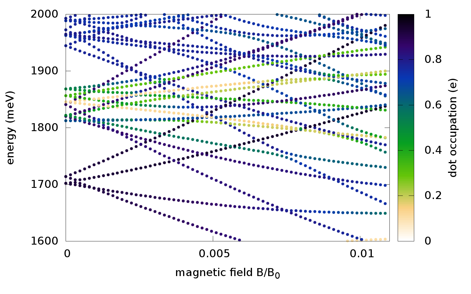
Applying an external magnetic field introduces a splitting of levels with opposite spin (and also valley). If we now gradually increase the magnetic field we obtain typical energy levels structure in a quantum dot with a magnetic field, presented in Fig 16. Similar structures are shown in [Pearce and Burkard, 2017] (or [Kormányos et al., 2014a]), calculated within the k.p model for -nm-size (or nm) MoS2 QD. However here we have more than 10 times smaller dot, thus to obtain similar orbital effects relatively to the magnetic scale (size of the Landau ground state), equal nm for T, we need to increase field more than 100 times. To keep the results in Fig. 16 comparable, we omit the Zeeman term here. Presented results are calculated for and mV, forming the QD confinement.
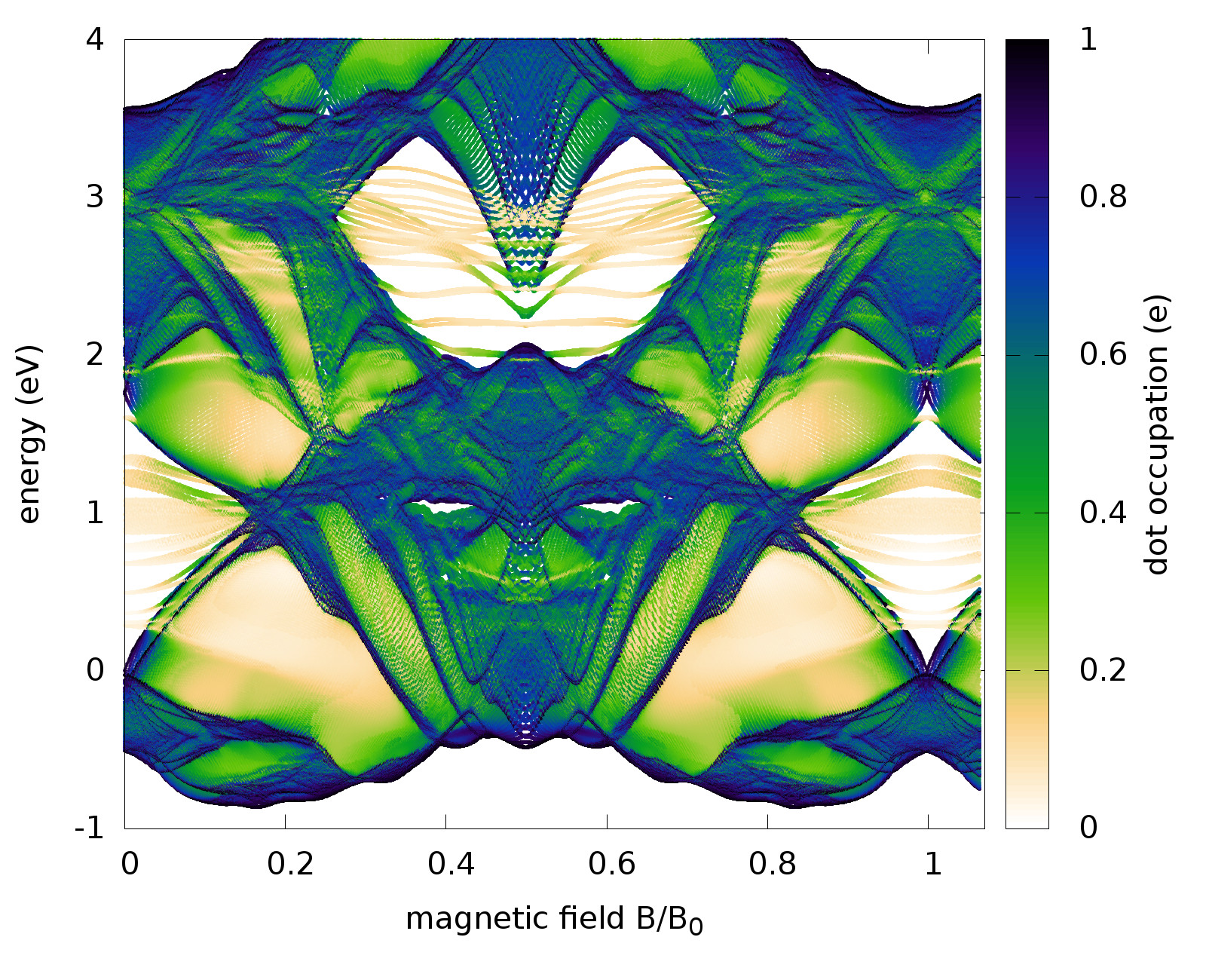
If we further increase the magnetic field, the energy levels will start to attract to each other and form characteristic Landau levels. Calculations for the whole range of artificially high magnetic fields , T, shows that Landau levels posses complicated self-similar structure, called the Hofstadter butterflyHofstadter (1976); Goldman (2009); Hunt et al. (2013); Wang et al. (2015). It is presented in Fig. 17. Complex regularities are also manifested in colors that represent the QD occupation. Same here we skip the Zeeman energy term.
Appendix C two-qubit gate matrices
Here we present the explicit forms of matrices representing the all two-qubit operations obtained in the simulations. They act in the 4-dimensional Hilbert space of the two-qubit spin-valley states . The first pair constitutes CNOT operations where the valley is the control qubit and the spin is the target one:
While in the second pair, the spin controlled valley-NOT operations are:
Finally, the SWAP and its complementary operations are given by:
Note that performing jointly both SWAP operations is equivalent to the NOT operation on the both qubits , i.e. .
References
- Wang et al. (2012) Q. H. Wang, K. Kalantar-Zadeh, A. Kis, J. N. Coleman, and M. S. Strano, Nature Nanotechnology 7, 699 (2012).
- Kormányos et al. (2014a) A. Kormányos, V. Zólyomi, N. D. Drummond, and G. Burkard, Phys. Rev. X 4, 011034 (2014a).
- Pawłowski et al. (2018) J. Pawłowski, D. Żebrowski, and S. Bednarek, Phys. Rev. B 97, 155412 (2018).
- Széchenyi et al. (2018) G. Széchenyi, L. Chirolli, and A. Pályi, 2D Materials 5, 035004 (2018).
- Rohling and Burkard (2012) N. Rohling and G. Burkard, New Journal of Physics 14, 083008 (2012).
- Wu et al. (2016) Y. Wu, Q. Tong, G.-B. Liu, H. Yu, and W. Yao, Phys. Rev. B 93, 045313 (2016).
- Papadopoulos et al. (2019) N. Papadopoulos, K. Watanabe, T. Taniguchi, H. S. J. van der Zant, and G. A. Steele, Phys. Rev. B 99, 115414 (2019).
- Shang et al. (2019) C. Shang, B. Lei, W. Zhuo, Q. Zhang, C. Zhu, J. Cui, X. Luo, N. Wang, F. Meng, L. Ma, et al., arXiv preprint arXiv:1902.09358 (2019).
- Paul et al. (2019) T. Paul, T. Ahmed, K. K. Tiwari, C. S. Thakur, and A. Ghosh, arXiv preprint arXiv:1904.03387 (2019).
- Pisoni et al. (2019) R. Pisoni, T. Davatz, K. Watanabe, T. Taniguchi, T. Ihn, and K. Ensslin, arXiv preprint arXiv:1904.09202 (2019).
- Ghiasi et al. (2019) T. S. Ghiasi, A. A. Kaverzin, P. J. Blah, and B. J. van Wees, arXiv preprint arXiv:1905.01371 (2019).
- Huang et al. (2018) W. Huang, X. Wang, X. Ji, Z. Zhang, and C. Jin, Nano Research 11, 5849 (2018).
- Kim et al. (2019a) Y. Kim, P. Herlinger, T. Taniguchi, K. Watanabe, and J. H. Smet, arXiv preprint arXiv:1903.10260 (2019a).
- Sahoo et al. (2019) P. K. Sahoo, S. Memaran, Y. Xin, T. D. Márquez, F. A. Nugera, Z. Lu, W. Zheng, N. D. Zhigadlo, D. Smirnov, L. Balicas, et al., arXiv preprint arXiv:1904.00311 (2019).
- Wang et al. (2018) K. Wang, K. D. Greve, L. A. Jauregui, A. Sushko, A. High, Y. Zhou, G. Scuri, T. Taniguchi, K. Watanabe, M. D. Lukin, H. Park, and P. Kim, Nature Nanotechnology 13, 128 (2018).
- Kim et al. (2019b) B.-K. Kim, D.-H. Choi, T.-H. Kim, H. Kim, K. Watanabe, T. Taniguchi, H. Rho, Y.-H. Kim, J.-J. Kim, and M.-H. Bae, arXiv preprint arXiv:1904.10295 (2019b).
- Reinhardt et al. (2019) S. Reinhardt, L. Pirker, C. Bäuml, M. Remškar, and A. K. Hüttel, arXiv preprint arXiv:1904.05972 (2019).
- Kotekar-Patil et al. (2019) D. Kotekar-Patil, J. Deng, S. L. Wong, and K. E. J. Goh, arXiv preprint arXiv:1904.06983 (2019).
- Zhang et al. (2017) Z.-Z. Zhang, X.-X. Song, G. Luo, G.-W. Deng, V. Mosallanejad, T. Taniguchi, K. Watanabe, H.-O. Li, G. Cao, G.-C. Guo, F. Nori, and G.-P. Guo, Science Advances 3, e1701699 (2017).
- Cortés et al. (2019) N. Cortés, O. Ávalos-Ovando, L. Rosales, P. A. Orellana, and S. E. Ulloa, Phys. Rev. Lett. 122, 086401 (2019).
- Zollner and Fabian (2019) K. Zollner and J. Fabian, arXiv preprint arXiv:1902.01631 (2019).
- Yuan et al. (2018) R.-Y. Yuan, Q.-J. Yang, and Y. Guo, Journal of Physics: Condensed Matter 30, 355301 (2018).
- Li et al. (2014) H. Li, J. Shao, D. Yao, and G. Yang, ACS Applied Materials & Interfaces 6, 1759 (2014).
- Majidi and Asgari (2014) L. Majidi and R. Asgari, Phys. Rev. B 90, 165440 (2014).
- Ilatikhameneh et al. (2015) H. Ilatikhameneh, Y. Tan, B. Novakovic, G. Klimeck, R. Rahman, and J. Appenzeller, IEEE Journal on Exploratory Solid-State Computational Devices and Circuits 1, 12 (2015).
- Georgiou et al. (2012) T. Georgiou, R. Jalil, B. D. Belle, L. Britnell, R. V. Gorbachev, S. V. Morozov, Y.-J. Kim, A. Gholinia, S. J. Haigh, O. Makarovsky, L. Eaves, L. A. Ponomarenko, A. K. Geim, K. S. Novoselov, and A. Mishchenko, Nature Nanotechnology 8, 100 (2012).
- Wu et al. (2019) D. Wu, W. Li, A. Rai, X. Wu, H. C. P. Movva, M. N. Yogeesh, Z. Chu, S. K. Banerjee, D. Akinwande, and K. Lai, Nano Letters 19, 1976 (2019).
- Ávalos-Ovando et al. (2019) O. Ávalos-Ovando, D. Mastrogiuseppe, and S. E. Ulloa, Phys. Rev. B 99, 035107 (2019).
- Choukroun et al. (2018) J. Choukroun, M. Pala, S. Fang, E. Kaxiras, and P. Dollfus, Nanotechnology 30, 025201 (2018).
- Marian et al. (2017) D. Marian, E. Dib, T. Cusati, E. G. Marin, A. Fortunelli, G. Iannaccone, and G. Fiori, Phys. Rev. Applied 8, 054047 (2017).
- Iannaccone et al. (2018) G. Iannaccone, F. Bonaccorso, L. Colombo, and G. Fiori, Nature Nanotechnology 13, 183 (2018).
- Laturia et al. (2018) A. Laturia, M. L. Van de Put, and W. G. Vandenberghe, npj 2D Materials and Applications 2, 6 (2018).
- Pawłowski et al. (2016) J. Pawłowski, P. Szumniak, and S. Bednarek, Phys. Rev. B 93, 045309 (2016).
- Rostami et al. (2013) H. Rostami, A. G. Moghaddam, and R. Asgari, Phys. Rev. B 88, 085440 (2013).
- Ridolfi et al. (2015) E. Ridolfi, D. Le, T. S. Rahman, E. R. Mucciolo, and C. H. Lewenkopf, Journal of Physics: Condensed Matter 27, 365501 (2015).
- Cappelluti et al. (2013) E. Cappelluti, R. Roldán, J. A. Silva-Guillén, P. Ordejón, and F. Guinea, Phys. Rev. B 88, 075409 (2013).
- Fang et al. (2015) S. Fang, R. Kuate Defo, S. N. Shirodkar, S. Lieu, G. A. Tritsaris, and E. Kaxiras, Phys. Rev. B 92, 205108 (2015).
- Liu et al. (2013) G.-B. Liu, W.-Y. Shan, Y. Yao, W. Yao, and D. Xiao, Phys. Rev. B 88, 085433 (2013).
- Kadantsev and Hawrylak (2012) E. S. Kadantsev and P. Hawrylak, Solid State Communications 152, 909 (2012).
- Ochoa and Roldán (2013) H. Ochoa and R. Roldán, Phys. Rev. B 87, 245421 (2013).
- Petersen and Hedegård (2000) L. Petersen and P. Hedegård, Surface Science 459, 49 (2000).
- Konschuh et al. (2010) S. Konschuh, M. Gmitra, and J. Fabian, Phys. Rev. B 82, 245412 (2010).
- Klinovaja and Loss (2013a) J. Klinovaja and D. Loss, Phys. Rev. X 3, 011008 (2013a).
- Klinovaja and Loss (2013b) J. Klinovaja and D. Loss, Phys. Rev. B 88, 075404 (2013b).
- Ezawa (2014) M. Ezawa, New Journal of Physics 16, 065015 (2014).
- Kane and Mele (2005) C. L. Kane and E. J. Mele, Phys. Rev. Lett. 95, 226801 (2005).
- Hofstadter (1976) D. R. Hofstadter, Physical Review B 14, 2239 (1976).
- Polizzi (2009) E. Polizzi, Phys. Rev. B 79, 115112 (2009).
- Dias et al. (2016) A. C. Dias, J. Fu, L. Villegas-Lelovsky, and F. Qu, Journal of Physics: Condensed Matter 28, 375803 (2016).
- Kormányos et al. (2014b) A. Kormányos, V. Zólyomi, N. D. Drummond, and G. Burkard, Phys. Rev. X 4, 039901 (2014b).
- Marinov et al. (2017) K. Marinov, A. Avsar, K. Watanabe, T. Taniguchi, and A. Kis, Nature Communications 8, 1938 (2017).
- Liu et al. (2014) G.-B. Liu, H. Pang, Y. Yao, and W. Yao, New Journal of Physics 16, 105011 (2014).
- Brey and Fertig (2006) L. Brey and H. A. Fertig, Phys. Rev. B 73, 235411 (2006).
- Zarenia et al. (2011) M. Zarenia, A. Chaves, G. A. Farias, and F. M. Peeters, Phys. Rev. B 84, 245403 (2011).
- Szafran et al. (2018a) B. Szafran, D. Żebrowski, and A. Mreńca-Kolasińska, Scientific Reports 8, 7166 (2018a).
- Szafran et al. (2018b) B. Szafran, A. Mreńca-Kolasińska, B. Rzeszotarski, and D. Żebrowski, Phys. Rev. B 97, 165303 (2018b).
- Rostami et al. (2016) H. Rostami, R. Asgari, and F. Guinea, Journal of Physics: Condensed Matter 28, 495001 (2016).
- Shi (2003) Y. Shi, Quantum Info. Comput. 3, 84 (2003).
- Zeuch et al. (2018) D. Zeuch, F. Hassler, J. Slim, and D. P. DiVincenzo, arXiv preprint arXiv:1807.02858 (2018).
- Rivera et al. (2016) P. Rivera, K. L. Seyler, H. Yu, J. R. Schaibley, J. Yan, D. G. Mandrus, W. Yao, and X. Xu, Science 351, 688 (2016).
- Pei et al. (2012) F. Pei, E. A. Laird, G. A. Steele, and L. P. Kouwenhoven, Nature Nanotechnology 7, 630 (2012).
- Laird et al. (2013) E. A. Laird, F. Pei, and L. P. Kouwenhoven, Nature Nanotechnology 8, 565 (2013).
- Osika and Szafran (2017) E. N. Osika and B. Szafran, Phys. Rev. B 95, 205305 (2017).
- Roldán et al. (2014) R. Roldán, M. P. López-Sancho, F. Guinea, E. Cappelluti, J. A. Silva-Guillén, and P. Ordejón, 2D Materials 1, 034003 (2014).
- Kośmider et al. (2013) K. Kośmider, J. W. González, and J. Fernández-Rossier, Phys. Rev. B 88, 245436 (2013).
- Löwdin (1962) P.-O. Löwdin, Journal of Mathematical Physics 3, 969 (1962).
- Bochevarov and Sherrill (2006) A. D. Bochevarov and C. D. Sherrill, Journal of Mathematical Chemistry 42, 59 (2006).
- Jin and Song (2011) L. Jin and Z. Song, Phys. Rev. A 83, 062118 (2011).
- Pavlović and Peeters (2015) S. Pavlović and F. M. Peeters, Phys. Rev. B 91, 155410 (2015).
- Pearce and Burkard (2017) A. J. Pearce and G. Burkard, 2D Materials 4, 025114 (2017).
- Goldman (2009) N. Goldman, Journal of Physics B: Atomic, Molecular and Optical Physics 42, 055302 (2009).
- Hunt et al. (2013) B. Hunt, J. D. Sanchez-Yamagishi, A. F. Young, M. Yankowitz, B. J. LeRoy, K. Watanabe, T. Taniguchi, P. Moon, M. Koshino, P. Jarillo-Herrero, and R. C. Ashoori, Science 340, 1427 (2013).
- Wang et al. (2015) L. Wang, Y. Gao, B. Wen, Z. Han, T. Taniguchi, K. Watanabe, M. Koshino, J. Hone, and C. R. Dean, Science 350, 1231 (2015).