Electrostatic Superlattices on Scaled Graphene Lattices
Abstract
A scalable tight-binding model is applied for large-scale quantum transport calculations in clean graphene subject to electrostatic superlattice potentials, including two types of graphene superlattices: moiré patterns due to the stacking of graphene and hexagonal boron nitride (hBN) lattices, and gate-controllable superlattices using a spatially modulated gate capacitance. In the case of graphene/hBN moiré superlattices, consistency between our transport simulation and experiment is satisfactory at zero and low magnetic field, but breaks down at high magnetic field due to the adopted simple model Hamiltonian that does not comprise higher-order terms of effective vector potential and Dirac mass terms. In the case of gate-controllable superlattices, no higher-order terms are involved, and the simulations are expected to be numerically exact. Revisiting a recent experiment on graphene subject to a gated square superlattice with periodicity of 35 nm, our simulations show excellent agreement, revealing the emergence of multiple extra Dirac cones at stronger superlattice modulation.
I Introduction
Graphene, a single layer of carbon atoms arranged in a honeycomb lattice, was first successfully isolated from a single crystal in 2004 Novoselov et al. (2004); Geim and Novoselov (2007), which subsequently triggered further investigations on the intriguing properties of relativistic Dirac fermions Castro Neto et al. (2009). However, to further uncover more novel electronic properties of the first truly two-dimensional material, the limited mobility of graphene on standard SiO2 substrates turned out to be the main factor restricting mean-free path and phase-coherence length. The discovery of hexagonal boron-nitride (hBN) as an ideal atomically flat substrate for graphene Dean et al. (2010) boosted the development of high-quality graphene devices. Fabrication of devices that involves the encapsulation of graphene between two thin hBN multilayers has become a standard protocol since then Yankowitz et al. (2019). At the same time, the combination of these two different 2D materials in a so-called van der Waals heterostructure Geim and Grigorieva (2013) led to the subsequent discovery of the graphene/hBN moiré pattern Yankowitz et al. (2012) arising from the large-scale lattice interference due to the slight lattice constant mismatch.
At small twist angles, the resulting moiré pattern provides a natural source of superlattice potential on graphene with periodicity in the order of , leading to the formation of new superlattice minibands in the electronic band structure of graphene at energies reachable by standard electrostatic gating. First experiments revealing new transport phenomena (such as the emergence of the Hofstadter butterfly) were reported in 2013 Ponomarenko et al. (2013); Dean et al. (2013); Hunt et al. (2013). In the following years, other exciting transport experiments have been reported Gorbachev et al. (2014); Wang et al. (2015a, b); Lee et al. (2016); Handschin et al. (2017); Krishna Kumar et al. (2017); Chen et al. (2017), as well as a dynamic band structure tuning Yankowitz et al. (2018); Ribeiro-Palau et al. (2018). More recently, another approach for inducing a superlattice potential in graphene has been demonstrated by using patterned dielectrics Forsythe et al. (2018). Such a gate-tunable superlattice structure allows for the design of arbitrary superlattice geometries with defined periodicity but suffers from technical restrictions.
On the theory side, most works related to graphene superlattices focus either on calculations for the superlattice-induced mini-band structures Park et al. (2008); Brey and Fertig (2009); Wu et al. (2012); Ortix et al. (2012); Kindermann et al. (2012); Wallbank et al. (2013); Moon and Koshino (2014), or on predicting transport properties by solving the Dirac equation with oversimplified superlattice model potential Barbier et al. (2010); Burset et al. (2011). On the other hand, quantum transport simulations considering realistic experimental conditions have been relatively rare in the literature Diez et al. (2014); Hu et al. (2018), not to mention a theory work combining quantum transport simulations and mini-band structure calculations, together with transport experiments. This work aims at providing a straightforward method to perform reliable quantum transport simulations, covering both graphene/hBN moiré superlattices and gate-induced superlattices. As shown in the following, our transport simulations based on the real-space Green’s function method for two-terminal structures as sketched in Figure 1(a) with the superlattice potential arising either from the graphene/hBN moiré pattern or from periodically modulated gating are consistent with transport experiments as well as mini-band structures based on the continuum model. Our method is applicable equally well to multi-terminal structures for simulating, for example, four-probe measurements using the Landauer-Büttiker approach Datta (1995).
This paper is organized as follows. In section II, we briefly introduce the theoretical methods used in section III, including graphene/hBN moiré superlattice (subsection III.1) and gate-induced superlattice (subsection III.2). A summary of this work is provided in section IV.
II Theoretical Approaches
II.1 Real-space tight-binding model for quantum transport
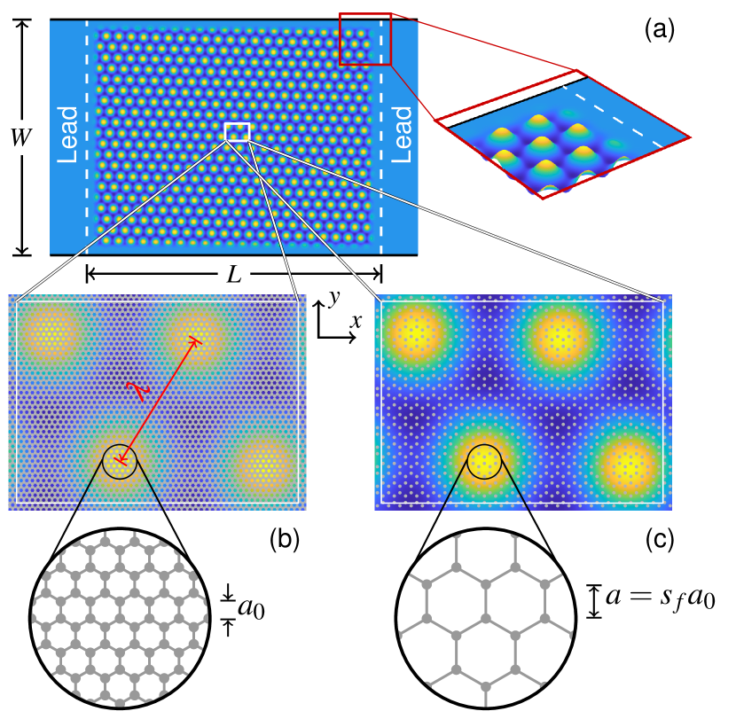
To perform quantum transport simulations for graphene working in real-space, the scalable tight-binding model Liu et al. (2015) has been proved to be a very convenient numerical trick (see, for example, Rickhaus et al. (2015); Mreńca-Kolasińska and Szafran (2016); Kolasiński et al. (2017); Petrović et al. (2017); Ma et al. (2018)): the physics of a graphene system can be captured by a graphene lattice scaled by a factor of such that the lattice spacing is given by with the carbon-carbon distance and the nearest neighbor hopping is with the hopping parameter for a genuine graphene lattice, as long as the scaled lattice spacing remains much shorter than all important physical length scales in the graphene system of interest.
In dealing with graphene superlattices, the newly introduced physical length scale not mentioned in Ref. Liu et al., 2015 is the periodicity of the superlattice. The advantage of the scaling can be easily appreciated by comparing Figure 1(b) and Figure 1(c): The former considers a genuine graphene lattice involving lots of carbon atoms, while the latter considers a scaled graphene lattice (here for illustrative purposes) involving a much reduced number of lattice sites. As long as is satisfied, a reasonably large area covering enough superlattice periods can be implemented in real-space quantum transport simulations to reveal transport properties arising from the superlattice effects.
The model Hamiltonian including the superlattice potential using the scaled graphene lattice can be written as
| (1) |
where the operator () annihilates (creates) an electron at site . The first term in Eq. (1) represents the clean part of the Hamiltonian which contains nearest neighbor hoppings summing over site indices and with standing for , and the second term is the on-site energy
| (2) |
containing the superlattice potential smoothed by a model function with , where is a smoothing parameter typically taken as . The purpose of smearing off the superlattice potential function to zero at a distance (typically taken as ) away from the edges and the leads [see Figure 1(a) and its inset] is to avoid any spurious effects due to the combination of the superlattice potential and the physical edges of the graphene lattice, as well as to avoid oversized unit cells for the lead self-energies. Any contributions to the on-site energy term other than the superlattice potential are collected in the term in Eq. (2).
With the model Hamiltonian Eq. (1) constructed, together with self-energies and describing the attached two leads (following, for example, Ref. Wimmer, 2008), the retarded Green’s function at energy is given by
| (3) |
leading to the transmission function
| (4) |
where with is the broadening function. In the low-temperature low-bias limit, the conductance across the modeled scattering region is given by the Landauer formula , where the factor of accounts for the spin degeneracy. For a pedagogical introduction to the above outlined real-space Green’s function, see, for example, Ref. Datta, 1995. Note that in most simulations, the full matrix of Eq. (3) is not needed, suggesting that a partial inversion should be implemented in the numerics to avoid wasting computer memories and CPU time. On the other hand, the matrix version of the Fisher-Lee relation (4) can be implemented as the way it reads.
II.2 Continuum model for mini-bands and density of states
To calculate the mini-band structure of graphene in the presence of a superlattice potential , we consider an infinitely large two-dimensional pristine graphene described by in -space. Following Ref. Park et al., 2008, we start with the continuum model Hamiltonian near the valley:
| (5) |
where the first term is and superlattice potential in the second term is treated as a perturbation. In Eq. (5), the product of the reduced Planck constant and Fermi velocity is related to the tight-binding parameters through , and the two-dimensional wave vector is small relative to the point. Using the eigenstates of as a new basis, we solve the eigenvalue problem of Eq. (5) to obtain a set of linear equations:
| (6) |
where is the energy eigenvalue of the graphene superlattice, is the eigenenergy of associated with the branch ( for electron above the Dirac point and for hole below the Dirac point), is the Fourier component of with the reciprocal lattice vector of the superlattice potential, is the angle from to , and are the expansion coefficients of the pristine graphene eigenstates.
The infinite-dimensional matrix spanned by the states with wave vectors in Eq. (6) allows for solving for and hence calculating the band structure. Since we focus on the low-energy region, a matrix involving states with and is found to be sufficient to attain the convergence of the band structure.
The density of states as a function of energy can be calculated by
| (7) |
where the integration is taken over the first Brillouin zone. Since is proportional to the number of energy eigenstates, it can be used to compare with the transport calculations.
III Electrostatic superlattices in graphene
III.1 Graphene/hBN moiré superlattices
Formation of the moiré pattern due to the stacking of hBN and graphene lattices has been understood in one of the earliest experiments Yankowitz et al. (2012). Following their model, the moiré pattern results in a triangular periodic scalar potential described by
| (8) |
where is the amplitude of the model potential and is the reciprocal primitive vector of the moiré pattern corresponding to the primitive vector in real space. The orientation angle and wavelength are related with those in real-space through and . The other two reciprocal vectors are given by and . Following Moon and Koshino (2014) with the zigzag lattice direction arranged along the axis, the moiré wavelength and the orientation angle of the pattern are given by
| (9) |
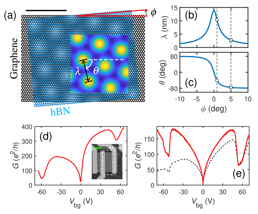
where is the graphene lattice constant, is the lattice constant mismatch with the hBN lattice constant, and is the twist angle of the hBN lattice relative to the graphene lattice. An illustrative example with is sketched in Fig. 2(a), where an overlay of given by Eq. (8) is shown to match perfectly the lattice structure of the resulting graphene/hBN moiré pattern. For completeness, and as functions of the twist angle are plotted in Figure 2(b) and (c), respectively, where the hollow squares mark the example of Figure 2(a) and the hollow circles mark the case corresponding to our transport experiments and simulations to be elaborated below.
According to Ref. Park et al., 2008, the expected secondary Dirac points in the presence of a triangular superlattice potential occur at the points of the hexagonal mini-Brillouin zone in space, with a distance to the point (where the normal Dirac point resides). Taking as an estimate for the corresponding carrier density , this suggests that the example of Fig. 1(a) with requires a density above , which is beyond a reasonable density range from typical electrostatic gating. Indeed, observable graphene/hBN superlattice effects are typically found only in nearly aligned graphene/hBN stacks with a very small twist angle. On the other hand, the points for the case of are expected at a density no more than , lying in the typical density range using standard electrostatic gating.
III.1.1 Transport at zero magnetic field
To test the validity of the quantum transport simulation illustrated in subsection II.1 using the above moiré superlattice model potential Eq. (8), we compare our simulations with the experimental results obtained from a two-terminal device based on a hBN/graphene/hBN stack on a Si/SiO2 substrate, where the crystallographic axis of the graphene flake is aligned with respect to one of the hBN flakes. Electric contact to the graphene is made from the edge of the mesa Wang et al. (2013) with self-aligned Ti/Al electrodes. We use the Si wafer as an overall back gate with a two-layer dielectric consisting of SiO2 with thickness and the bottom hBN flake with thickness . A typical exemplary junction similar to the measured device is shown by the atomic-force mircroscope (AFM) image in the inset of Fig. 2(d) and marked by the white dashed box. Figure 2(d) shows the two-terminal differential conductance of our sample as a function of the back gate voltage , measured at low temperature (), using standard low-frequency () lock-in technique.
To simulate such a conductance measurement, we have calculated the transmission as a function of Fermi energy at zero temperature, and hence the conductance , based on a tight-binding model Hamiltonian, for a two-terminal device similar to Figure 1(a) with , implementing the moiré model potential (8) with a twist angle . To compare with the experiment on the same voltage axis, we adopt the parallel-plate capacitor formula for the carrier density, , and relate with the Fermi energy through . These give us
| (10) |
where is the back gate capacitance per unit area with . Using this capacitance value, the exhibiting conductance dips at and observed in Figure 2(d) correspond to densities about and , respectively, so that the twist angle is estimated to lie in the range of . Indeed, when choosing for the moiré model potential Eq. (8), the simulated conductance transformed from and reported in Figure 2(e) is found to show excellent agreement with the experiment Figure 2(d) in the positions of the conductance dips.
Note that the red curve reported in Figure 2(e) considers leads with on-site and Fermi energies identical to those at the attaching lattice sites; see Figure 1(a). Compared to Figure 2(d), the electron-hole asymmetry is less pronounced due to the simple model of Eq. (8) from Ref. Yankowitz et al., 2012. Although accounting for an electron doping from the metal leads simply by fixing the Fermi energy in the leads with a positive value can make the conductance curve [black dashed curve in Figure 2(e) with Fermi energy in the leads] even more similar to the experiment, the nature of the electron-hole asymmetry observed in Figure 2(d) comes from higher-order terms such as the effective vector potential and Dirac mass terms Kindermann et al. (2012); Wallbank et al. (2013); Moon and Koshino (2014) needed for a model Hamiltonian that can better describe the graphene/hBN moiré superlattice. We will continue our discussions with calculations based on leads with “floating” Fermi energies.
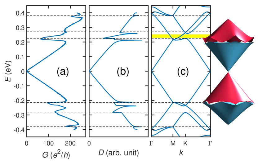
Without transforming to the gate voltage axis, the original conductance data of Figure 2(e) as a function of energy is reported in Figure 3(a) with a wider energy range up to . Compared to the density of states [Figure 3(b)] and the band structure [Figure 3(c)] which are calculated based on the same moiré superlattice model potential but within the continuum model (subsection II.2), consistent features in the energy spectrum can be seen. In view of Figure 2(d)–(e) and Figure 3, our calculations significantly capture some of the basic properties of the graphene/hBN moiré superlattice, at least at zero magnetic field.
III.1.2 Transport at finite magnetic field
We continue our comparison of the experimentally measured and theoretically calculated conductance with, however, finite magnetic field perpendicular to the graphene plane, which can be modeled by associating the Peierls phase Peierls (1933); Datta (1995) to the hopping in Eq. (1), where , choosing the Landau gauge for the vector potential ; see the axes shown in Figure 1. Conductance maps of are reported in Figure 4(a)/(b) from the experiment/theory showing magnetic field up to and the gate voltage range same as Figure 2(d)/(e). Note that the red curves of Figure 2(d)/(e) correspond exactly to the horizontal line cuts at of Figure 4(a)/(b). Within the gate voltage range of about , typical relativistic Landau fans can be seen in both experiment and theory. To have a closer look, we magnify the regions marked by the black dashed box on Figure 4(a)/(b) in Figure 4(c)/(d) with a different color map to highlight the quantized conductance plateaus. Numbers on Figure 4(d) label the filling factor on the corresponding plateau with the expected conductance . Good agreement between experiment [Figure 4(a) and (c)] and theory [Figure 4(b) and (d)] within the main Dirac cone can be seen.
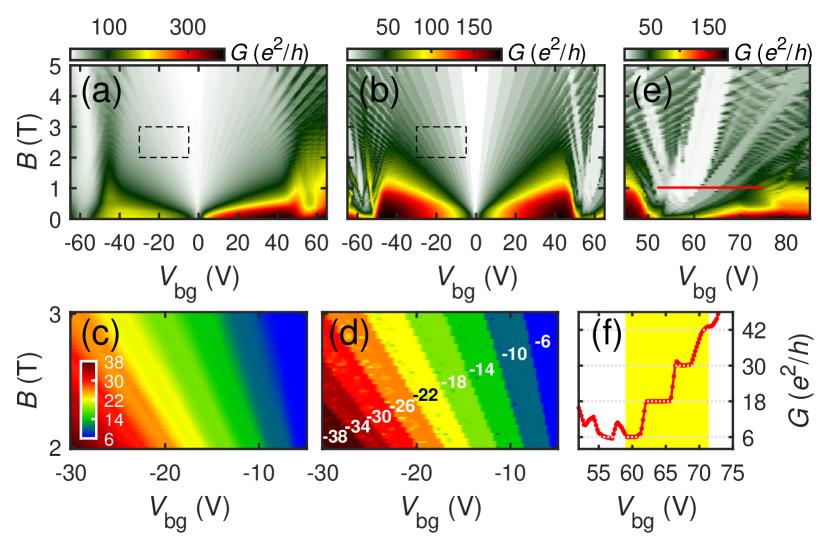
At gate voltages , transport properties are dominated by the extra Dirac cones arising from the modulating moiré superlattice. Discrepancies between the experiment and theory are self-evident. This suggests that the neglected higher-order terms of a more complete model Hamiltonian (see, for example, Refs. Kindermann et al., 2012; Wallbank et al., 2013; Moon and Koshino, 2014) become important when the magnetic field is strong. Interestingly, we note that in the theory map of Figure 4(b), some unusual plateaus in the energy range around the electron-branch secondary Dirac point can be observed. We magnify this region in Figure 4(e) with a horizontal line cut shown in Figure 4(f), where the gate voltage range showing quantized conductance plateaus is highlighted by a yellow background.
This range, transformed back to the energy through Eq. (10), corresponds to an energy window where part of the electron branch of the secondary Dirac cones at points of the superlattice mini-Brillouin zone are completely isolated. The respective energy window is highlighted also by yellow in Figure 3(c). Since there are effectively 3 such Dirac cones (six cones on six points within each mini-Brillouin zone but each cone shared by two neighboring mini-Brillouin zones), the degeneracy factor is expected to be with accounting for spin and another for valley. Indeed, in the quantum Hall regime, the calculated conductance is quantized to as shown in Figure 4(f). Outside this energy (and hence back gate voltage) range, the higher-order Dirac cones are always mixed with background bands, so that no quantized conductance is observed. However, such special energy window leading to the -fold-degeneracy of the Landau levels at the secondary DP is never observed in transport experiments with graphene/hBN moiré superlattices Ponomarenko et al. (2013); Dean et al. (2013); Lee et al. (2016); Handschin et al. (2017); Krishna Kumar et al. (2017), including ours shown in Figure 2(d), indicating once again that the simplified model of Eq. (8) containing only the electrostatic scalar potential term is not sufficient to capture transport properties of graphene/hBN moiré superlattices at high magnetic fields, i.e. in the quantum Hall regime. As we will see below, when the graphene superlattice potential comes solely from the electrostatic gating, our method becomes exact because in that system no such higher order terms are involved.
III.2 Gate-controlled superlattices
To observe any superlattice effects in graphene, the mean free path must be able to cover enough periods of the superlattice potential. This means, either the sample quality must be extraordinary, or the superlattice periodicity must be short enough. When the periodicity is too short, however, the resulting extra Dirac cones appear at too high energy, exceeding the experimentally reachable range. This is why the discovery of the graphene/hBN moiré pattern Yankowitz et al. (2012) led to first of its kind studies on graphene superlattices – the periodicity corresponding to small twist angles turns out to be naturally in a suitable range for experiments; see Figure 2(b). On the other hand, the superimposed superlattice potential due to the graphene/hBN moiré pattern is defined as a hexagonal lattice emerging from the two host lattices.
A more flexible approach to design artificial graphene superlattice structures for band structure engineering was pursued with the realization of electrostatic gating schemes Forsythe et al. (2018). To create an externally controllable periodic potential, the most intuitive way is to pattern an array of periodic fine metal gates on top of the graphene sample Dubey et al. (2013); Drienovsky et al. (2014). However, due to technical difficulties such as instabilities of nanometer-scale local gates, the low adhesion between metal gates and the inert hBN, etc., such superlattice graphene devices often suffer the problem of very low sample yield Drienovsky et al. (2017). The basic idea of the new technical breakthrough is to keep the hBN/graphene/hBN sandwich intact, while periodically modulating the gate capacitance. This can be achieved either by using few-layer graphene as a local gate which is subsequently etched with a periodic pattern Drienovsky et al. (2017, 2018), or by etching the dielectric layer with a periodic pattern using a standard uniform back gate underneath the modulated substrate Forsythe et al. (2018). The latter will be our focus in the rest of this section.
Following the geometry of the device subject to a square superlattice potential with periodicity presented in Ref. Forsythe et al., 2018, we have performed our own electrostatic simulation to obtain the back gate capacitance showing periodic spatial modulation. We consider an hBN/graphene/hBN sandwich (showing no measurable moiré superlattice effects) gated by a global top gate contributing a uniform carrier density , and a bottom gate at voltage with a pre-patterned SiO2 substrate in between. See Fig. 1 of Ref. Forsythe et al., 2018. The bottom gate capacitance therefore shows a spatial modulation with a square lattice symmetry, as shown in the lower left inset of Figure 5(a).
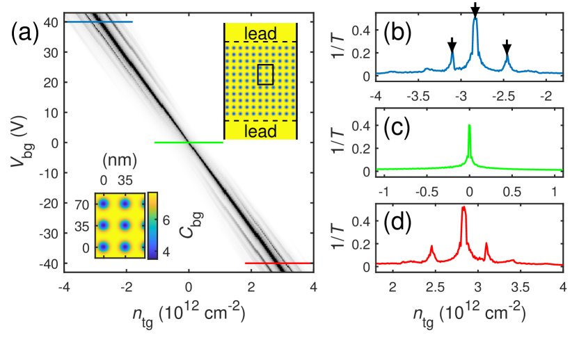
With the electrostatically simulated position-dependent back gate capacitance per unit area , contributing carrier density , together with the uniform , the resulting superlattice potential is given by with , in order to set the global transport Fermi level at zero Liu and Richter (2012). Slightly different from the case of the graphene/hBN moiré superlattice (subsection III.1) where the model potential given by Eq. (8) is independent of the gating, we consider for the on-site energy term (2), and implement it in the tight-binding Hamiltonian (1) with to perform quantum transport simulations over a two-terminal structure with and ; see the upper right inset of Figure 5(a).
To compare with the resistance measurements reported in Ref. Forsythe et al., 2018, we plot the inverse transmission as a function of and in the main panel of Figure 5(a), where most areas show high transmission (white regions correspond to low ). Along the diagonal dark thick line showing high values due to the main Dirac point, multiple satellite peaks can be seen when increasing and hence the magnitude of the square superlattice potential, signifying the emerging multiple extra Dirac points due to the gate-controlled square superlattice potential. Exemplary line cuts are plotted in Figure 5(b)–(d) to show clearly the single- and multiple-peak structures, in excellent agreement with the experiment Forsythe et al. (2018).
We have also checked the consistency between the calculated mini-band structures and the simulated inverse transmission. Overall, we obtain band structures similar to that reported in Ref. Forsythe et al., 2018, but since each point corresponds to a different profile and hence a different mini-band structure, an overview consistency-check like in Figure 3 is technically not possible. Instead, the consistency can be checked by comparing the peaks and their corresponding mini-band structure around . We have chosen three particular configurations corresponding to the three black arrows in Figure 5(b) marking three of the peaks, at which the Fermi level is expected to hit either the main or the extra Dirac points.
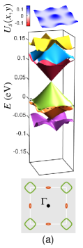
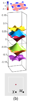
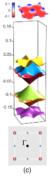
These mini-band structures, along with the actual profiles implemented individually in the continuum model (subsection II.2) are shown in Figure 6. Going from low to high [left, middle, and right black arrow in Figure 5(b)], the highest filled energy rises relative to the main Dirac point, corresponding to the sinking of the whole band structure due to our choice of fixing the Fermi level at [Figure 6(a), (b), and (c)]. As expected, the highest peak in Figure 5(b) marked by the middle black arrow corresponds to Figure 6(b), where the main Dirac point is nearly hit; see the lower sub-panel therein and the relevant caption. From the Fermi contours of Figure 6(a) and (c), the two satellite peaks seen in Figure 5(b) are mainly contributed by the secondary Dirac points at , labeling the midpoints on the edges of the square mini-Brillouin zone.
Note that the mini-band structures shown in Figure 6, though corresponding to an increasing uniform , do not exhibit simply an energy shift without changing the band shape. Compare, for example, the shapes of the lowest subbands. In addition, in this simulated case, no energy windows accommodating completely isolated extra Dirac points can be found. We note, however, that by properly designing the gate capacitance geometry, it is possible to find isolated extra Dirac points, even at . When isolated extra Dirac points are found, electronic transport is supported solely by the isolated extra Dirac cone, and more novel transport properties of band-engineered graphene superlattices can be explored. This is beyond the scope of the present work and is left as a future direction to further elaborate.
IV Concluding Remarks
In summary, we have shown that quantum transport simulations based on the scalable tight-binding model Liu et al. (2015) correctly capture transport properties of electrostatic graphene superlattices. In the case of graphene/hBN moiré superlattice (subsection III.1), the consistency of our simulation and experiment at zero and low magnetic field is rather satisfactory but breaks down at strong magnetic field due to the neglected higher-order terms in a more complete model Hamiltonian Kindermann et al. (2012); Wallbank et al. (2013); Moon and Koshino (2014). In the other case of gated superlattices (subsection III.2), without such higher order terms the simulations are expected to be exact. Indeed, compared to the transport experiment with a gate-controlled square superlattice reported in Ref. Forsythe et al., 2018, our simulations show an excellent agreement in revealing the emergence of multiple extra Dirac cones at zero magnetic field. Transport simulations at finite magnetic field for the gated superlattices are expected to reveal also consistent behaviors compared to the experiment, but are left as a future work.
Our work shows that real-space transport simulations based on the scalable tight-binding model Liu et al. (2015) can be extended to treat electrostatic superlattices, whether of the graphene/hBN type or the modulated gate capacitance type, providing consistent results compared to experiments. The method can be immediately applied to take into account, for example, complex local gating or multi-probe transport, in order to make further analysis for transport experiments or even reliable predictions. We note some recent studies working on developing numerical techniques that allow large-scale efficient transport simulations Beconcini et al. (2016); Calogero et al. (2018); Papior et al. (2019), but scaling the graphene lattices with an appropriately chosen scaling factor depending on the superlattice periodicity seems to be of least technical complexity and is readily applicable to anyone who is familiar with quantum transport using, for example, real-space Green’s function method Datta (1995) or the popular open-source python package KWANT Groth et al. (2014).
Acknowledgements.
We thank R. Huber, J. Eroms, and C. J. Kent for valuable and stimulating discussions. Financial supports from Taiwan Minister of Science and Technology (grant No. 107-2112-M-006-004-MY3), Deutsche Forschungsgemeinschaft (projects A07 and Ri681/13-1 under SFB 1277), and Helmholtz Society (program STN) are gratefully acknowledged.References
- Novoselov et al. (2004) K. S. Novoselov, A. K. Geim, S. V. Morozov, D. Jiang, Y. Zhang, S. V. Dubonos, I. V. Grigorieva, and A. A. Firsov, Electric Field Effect in Atomically Thin Carbon Films, Science 306, 666 (2004).
- Geim and Novoselov (2007) A. K. Geim and K. S. Novoselov, The rise of graphene, Nat. Mater. 6, 183 (2007).
- Castro Neto et al. (2009) A. H. Castro Neto, F. Guinea, N. M. R. Peres, K. S. Novoselov, and A. K. Geim, The electronic properties of graphene, Rev. Mod. Phys. 81, 109 (2009).
- Dean et al. (2010) C. R. Dean, A. F. Young, I. Meric, C. Lee, L. Wang, S. Sorgenfrei, K. Watanabe, T. Taniguchi, P. Kim, K. L. Shepard, and J. Hone, Boron nitride substrates for high-quality graphene electronics, Nat. Nano. 5, 722 (2010).
- Yankowitz et al. (2019) M. Yankowitz, Q. Ma, P. Jarillo-Herrero, and B. J. LeRoy, van der waals heterostructures combining graphene and hexagonal boron nitride, Nature Reviews Physics 1, 112 (2019).
- Geim and Grigorieva (2013) A. K. Geim and I. V. Grigorieva, Van der waals heterostructures, Nature 499, 419 EP (2013), perspective.
- Yankowitz et al. (2012) M. Yankowitz, J. Xue, D. Cormode, J. D. Sanchez-Yamagishi, K. Watanabe, T. Taniguchi, P. Jarillo-Herrero, P. Jacquod, and B. J. LeRoy, Emergence of superlattice dirac points in graphene on hexagonal boron nitride, Nat. Phys. 8, 382 (2012).
- Ponomarenko et al. (2013) L. Ponomarenko, R. Gorbachev, G. Yu, D. Elias, R. Jalil, A. Patel, A. Mishchenko, A. Mayorov, C. Woods, J. Wallbank, et al., Cloning of dirac fermions in graphene superlattices, Nature 497, 594 (2013).
- Dean et al. (2013) C. Dean, L. Wang, P. Maher, C. Forsythe, F. Ghahari, Y. Gao, J. Katoch, M. Ishigami, P. Moon, M. Koshino, et al., Hofstadter/’s butterfly and the fractal quantum hall effect in moire superlattices, Nature 497, 598 (2013).
- Hunt et al. (2013) B. Hunt, J. D. Sanchez-Yamagishi, A. F. Young, M. Yankowitz, B. J. LeRoy, K. Watanabe, T. Taniguchi, P. Moon, M. Koshino, P. Jarillo-Herrero, and R. C. Ashoori, Massive dirac fermions and hofstadter butterfly in a van der waals heterostructure, Science 340, 1427 (2013).
- Gorbachev et al. (2014) R. V. Gorbachev, J. C. W. Song, G. L. Yu, A. V. Kretinin, F. Withers, Y. Cao, A. Mishchenko, I. V. Grigorieva, K. S. Novoselov, L. S. Levitov, and A. K. Geim, Detecting topological currents in graphene superlattices, Science 346, 448 (2014).
- Wang et al. (2015a) L. Wang, Y. Gao, B. Wen, Z. Han, T. Taniguchi, K. Watanabe, M. Koshino, J. Hone, and C. R. Dean, Evidence for a fractional fractal quantum hall effect in graphene superlattices, Science 350, 1231 (2015a).
- Wang et al. (2015b) P. Wang, B. Cheng, O. Martynov, T. Miao, L. Jing, T. Taniguchi, K. Watanabe, V. Aji, C. N. Lau, and M. Bockrath, Topological winding number change and broken inversion symmetry in a hofstadter’s butterfly, Nano Letters 15, 6395 (2015b).
- Lee et al. (2016) M. Lee, J. R. Wallbank, P. Gallagher, K. Watanabe, T. Taniguchi, V. I. Falko, and D. Goldhaber-Gordon, Ballistic miniband conduction in a graphene superlattice, Science 353, 1526 (2016).
- Handschin et al. (2017) C. Handschin, P. Makk, P. Rickhaus, M.-H. Liu, K. Watanabe, T. Taniguchi, K. Richter, and C. Schönenberger, Fabry-pérot resonances in a graphene/hbn moiré superlattice, Nano Lett. 17, 328 (2017).
- Krishna Kumar et al. (2017) R. Krishna Kumar, X. Chen, G. H. Auton, A. Mishchenko, D. A. Bandurin, S. V. Morozov, Y. Cao, E. Khestanova, M. Ben Shalom, A. V. Kretinin, K. S. Novoselov, L. Eaves, I. V. Grigorieva, L. A. Ponomarenko, V. I. Fal’ko, and A. K. Geim, High-temperature quantum oscillations caused by recurring bloch states in graphene superlattices, Science 357, 181 (2017).
- Chen et al. (2017) G. Chen, M. Sui, D. Wang, S. Wang, J. Jung, P. Moon, S. Adam, K. Watanabe, T. Taniguchi, S. Zhou, M. Koshino, G. Zhang, and Y. Zhang, Emergence of tertiary dirac points in graphene moiré superlattices, Nano Letters 17, 3576 (2017).
- Yankowitz et al. (2018) M. Yankowitz, J. Jung, E. Laksono, N. Leconte, B. L. Chittari, K. Watanabe, T. Taniguchi, S. Adam, D. Graf, and C. R. Dean, Dynamic band-structure tuning of graphene moiré superlattices with pressure, Nature 557, 404 (2018).
- Ribeiro-Palau et al. (2018) R. Ribeiro-Palau, C. Zhang, K. Watanabe, T. Taniguchi, J. Hone, and C. R. Dean, Twistable electronics with dynamically rotatable heterostructures, Science 361, 690 (2018).
- Forsythe et al. (2018) C. Forsythe, X. Zhou, K. Watanabe, T. Taniguchi, A. Pasupathy, P. Moon, M. Koshino, P. Kim, and C. R. Dean, Band structure engineering of 2d materials using patterned dielectric superlattices, Nat. Nanotechnol. 13, 566 (2018).
- Park et al. (2008) C.-H. Park, L. Yang, Y.-W. Son, M. L. Cohen, and S. G. Louie, New generation of massless dirac fermions in graphene under external periodic potentials, Phys. Rev. Lett. 101, 126804 (2008).
- Brey and Fertig (2009) L. Brey and H. A. Fertig, Emerging zero modes for graphene in a periodic potential, Phys. Rev. Lett. 103, 046809 (2009).
- Wu et al. (2012) S. Wu, M. Killi, and A. Paramekanti, Graphene under spatially varying external potentials: Landau levels, magnetotransport, and topological modes, Phys. Rev. B 85, 195404 (2012).
- Ortix et al. (2012) C. Ortix, L. Yang, and J. van den Brink, Graphene on incommensurate substrates: Trigonal warping and emerging dirac cone replicas with halved group velocity, Phys. Rev. B 86, 081405 (2012).
- Kindermann et al. (2012) M. Kindermann, B. Uchoa, and D. L. Miller, Zero-energy modes and gate-tunable gap in graphene on hexagonal boron nitride, Phys. Rev. B 86, 115415 (2012).
- Wallbank et al. (2013) J. R. Wallbank, A. A. Patel, M. Mucha-Kruczyński, A. K. Geim, and V. I. Fal’ko, Generic miniband structure of graphene on a hexagonal substrate, Phys. Rev. B 87, 245408 (2013).
- Moon and Koshino (2014) P. Moon and M. Koshino, Electronic properties of graphene/hexagonal-boron-nitride moiré superlattice, Phys. Rev. B 90, 155406 (2014).
- Barbier et al. (2010) M. Barbier, P. Vasilopoulos, and F. M. Peeters, Extra Dirac points in the energy spectrum for superlattices on single-layer graphene, Phys. Rev. B 81, 075438 (2010).
- Burset et al. (2011) P. Burset, A. L. Yeyati, L. Brey, and H. A. Fertig, Transport in superlattices on single-layer graphene, Phys. Rev. B 83, 195434 (2011).
- Diez et al. (2014) M. Diez, J. P. Dahlhaus, M. Wimmer, and C. W. J. Beenakker, Emergence of massless dirac fermions in graphene’s hofstadter butterfly at switches of the quantum hall phase connectivity, Phys. Rev. Lett. 112, 196602 (2014).
- Hu et al. (2018) J. Hu, A. F. Rigosi, J. U. Lee, H.-Y. Lee, Y. Yang, C.-I. Liu, R. E. Elmquist, and D. B. Newell, Quantum transport in graphene junctions with moiré superlattice modulation, Phys. Rev. B 98, 045412 (2018).
- Datta (1995) S. Datta, Electronic Transport in Mesoscopic Systems (Cambridge University Press, Cambridge, 1995).
- Liu et al. (2015) M.-H. Liu, P. Rickhaus, P. Makk, E. Tóvári, R. Maurand, F. Tkatschenko, M. Weiss, C. Schönenberger, and K. Richter, Scalable Tight-Binding Model for Graphene, Phys. Rev. Lett. 114, 036601 (2015).
- Rickhaus et al. (2015) P. Rickhaus, P. Makk, M.-H. Liu, E. Tóvári, M. Weiss, R. Maurand, K. Richter, and C. Schönenberger, Snake trajectories in ultraclean graphene p-n junctions, Nat. Commun. 6, 6470 (2015).
- Mreńca-Kolasińska and Szafran (2016) A. Mreńca-Kolasińska and B. Szafran, Lorentz force effects for graphene aharonov-bohm interferometers, Phys. Rev. B 94, 195315 (2016).
- Kolasiński et al. (2017) K. Kolasiński, A. Mreńca-Kolasińska, and B. Szafran, Imaging snake orbits at graphene n-p junctions, Phys. Rev. B 95, 045304 (2017).
- Petrović et al. (2017) M. D. Petrović, S. P. Milovanović, and F. M. Peeters, Scanning gate microscopy of magnetic focusing in graphene devices: quantum versus classical simulation, Nanotechnology 28, 185202 (2017).
- Ma et al. (2018) Q. Ma, F. D. Parmentier, P. Roulleau, and G. Fleury, Graphene n-p junctions in the quantum hall regime: Numerical study of incoherent scattering effects, Phys. Rev. B 97, 205445 (2018).
- Wimmer (2008) M. Wimmer, Quantum transport in nanostructures: From computational concepts to spintronics in graphene and magnetic tunnel junctions, Ph.D. thesis, Universität Regensburg (2008).
- Wang et al. (2013) L. Wang, I. Meric, P. Y. Huang, Q. Gao, Y. Gao, H. Tran, T. Taniguchi, K. Watanabe, L. M. Campos, D. A. Muller, J. Guo, P. Kim, J. Hone, K. L. Shepard, and C. R. Dean, One-dimensional electrical contact to a two-dimensional material, Science 342, 614 (2013).
- Peierls (1933) R. Peierls, Zur Theorie des Diamagnetismus von Leitungselektronen, Zeitschrift für Physik A Hadrons and Nuclei 80, 763 (1933), 10.1007/BF01342591.
- Dubey et al. (2013) S. Dubey, V. Singh, A. K. Bhat, P. Parikh, S. Grover, R. Sensarma, V. Tripathi, K. Sengupta, and M. M. Deshmukh, Tunable Superlattice in Graphene To Control the Number of Dirac Points, Nano Lett. 13, 3990 (2013).
- Drienovsky et al. (2014) M. Drienovsky, F.-X. Schrettenbrunner, A. Sandner, D. Weiss, J. Eroms, M.-H. Liu, F. Tkatschenko, and K. Richter, Towards superlattices: Lateral bipolar multibarriers in graphene, Phys. Rev. B 89, 115421 (2014).
- Drienovsky et al. (2017) M. Drienovsky, A. Sandner, C. Baumgartner, M.-H. Liu, T. Taniguchi, K. Watanabe, K. Richter, D. Weiss, and J. Eroms, Few-layer graphene patterned bottom gates for van der Waals heterostructures, arXiv:1703.05631 (2017).
- Drienovsky et al. (2018) M. Drienovsky, J. Joachimsmeyer, A. Sandner, M.-H. Liu, T. Taniguchi, K. Watanabe, K. Richter, D. Weiss, and J. Eroms, Commensurability oscillations in one-dimensional graphene superlattices, Phys. Rev. Lett. 121, 026806 (2018).
- Liu and Richter (2012) M.-H. Liu and K. Richter, Efficient quantum transport simulation for bulk graphene heterojunctions, Phys. Rev. B 86, 115455 (2012).
- Beconcini et al. (2016) M. Beconcini, S. Valentini, R. K. Kumar, G. H. Auton, A. K. Geim, L. A. Ponomarenko, M. Polini, and F. Taddei, Scaling approach to tight-binding transport in realistic graphene devices: The case of transverse magnetic focusing, Phys. Rev. B 94, 115441 (2016).
- Calogero et al. (2018) G. Calogero, N. R. Papior, P. Bøggild, and M. Brandbyge, Large-scale tight-binding simulations of quantum transport in ballistic graphene, Journal of Physics: Condensed Matter 30, 364001 (2018).
- Papior et al. (2019) N. Papior, G. Calogero, S. Leitherer, and M. Brandbyge, Removing all periodic boundary conditions: Efficient non-equilibrium Green function calculations, arXiv:1905.11113 (2019).
- Groth et al. (2014) C. W. Groth, M. Wimmer, A. R. Akhmerov, and X. Waintal, Kwant: a software package for quantum transport, New Journal of Physics 16, 063065 (2014).