The high voltage system with pressure and temperature corrections for the novel MPGD-based photon detectors of COMPASS RICH-1
Abstract
The novel MPGD-based photon detectors of COMPASS RICH-1 consist of large-size hybrid MPGDs with multi-layer architecture including two layers of Thick-GEMs and a bulk resistive MicroMegas. The top surface of the first THGEM is coated with a CsI film which also acts as photo-cathode. These detectors have been successfully in operation at COMPASS since 2016. Concerning bias-voltage supply, the Thick-GEMs are segmented in order to reduce the energy released in case of occasional discharges, while the MicroMegas anode is segmented into pads individually biased with positive voltage while the micromesh is grounded. In total, there are about ten different electrode types and more than 20000 electrodes supplied by more than 100 HV channels, where appropriate correlations among the applied voltages are required for the correct operation of the detectors. Therefore, a robust control system is mandatory, implemented by a custom designed software package, while commercial power supply units are used. This sophisticated control system allows to protect the detectors against errors by the operator, to monitor and log voltages and currents at 1 Hz rate, and automatically react to detector misbehaviour. In addition, a voltage compensation system has been developed to automatically adjust the biasing voltage according to environmental pressure and temperature variations, to achieve constant gain over time. This development answers to a more general need. In fact, voltage compensation is always a requirement for the stability of gaseous detectors and its need is enhanced in multi-layer ones.
In this paper, the HV system and its performance are described in details, as well as the stability of the novel MPGD-based photon detectors during the physics data taking at COMPASS.
keywords:
MPGD , HV system , Pressure and Temperature corrections , gain , COMPASS , RICH-11 Introduction
The RICH-1 detector [1, 2, 3] of the COMPASS experiment [4, 5] is a Ring Imaging Cherenkov detector with a 3 m long gaseous C4F10 radiator, 21 m2 wide focusing VUV mirror surface and Photon Detectors (PD) covering a total active area of 5.5 m2. In the 2015-2016 winter shut-down of the COMPASS experiment, around 1.4 m2 of the active area of the photon detectors was upgraded by novel detectors based on MPGD technologies [6]. Four new PDs (unit size: 600600 mm2) replace the previously used MWPC-based PDs in order to cope with the challenging efficiency and stability requirements of the new COMPASS measurements. In fact, COMPASS goal is to deal with trigger rates up to O(105) Hz and beam rates up to O(108) Hz and the new detector architecture guarantees data taking stability.
The high voltage system for the upgraded detectors and its performance, as well as its significance on the detector stability are the focus of this paper.
| Electrode | Protection | Drift | THGEM1 | THGEM1 | THGEM2 | THGEM2 | mesh | MM anode |
|---|---|---|---|---|---|---|---|---|
| wire plane | wire plane | top | bottom | top | bottom | |||
| Voltage | -300 V | -3520 V | -3320 V | -2050 V | -1750 V | -500 V | grounded | +620 V |
| Number of | ||||||||
| HV channels | 1 | 1 | 4 | 4 | 4 | 4 | 0 | 4 |
| per detector |
2 The architecture of the photon detectors
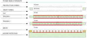
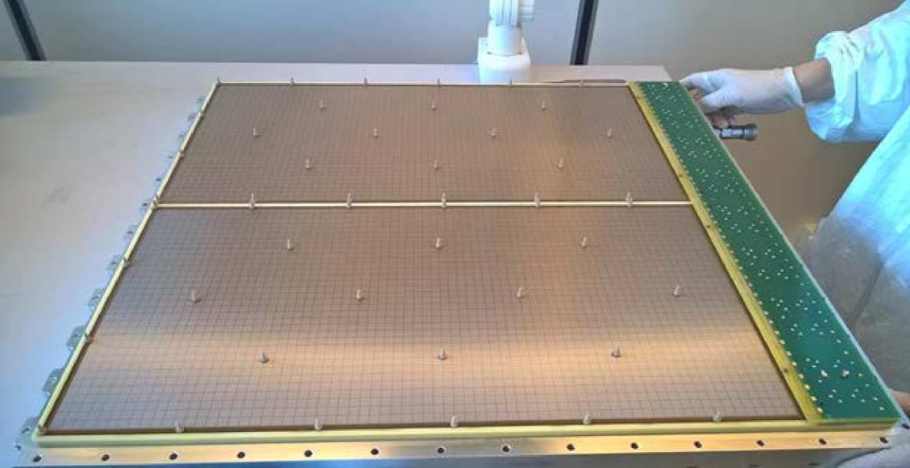
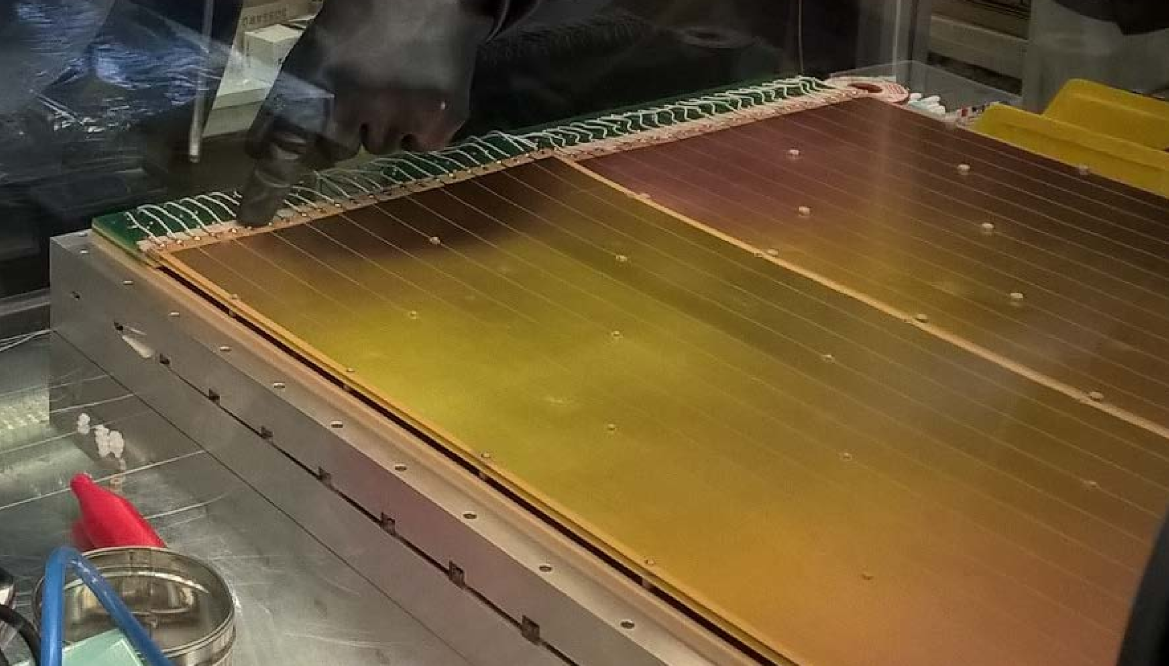
The architecture of the novel detectors results from a seven-year R&D activity [7, 8, 9, 10] and it concludes in a hybrid MPGD arrangement (Fig. 1): two layers of THick GEMs (THGEM) [11, 12, 13, 14] are coupled to a MicroMegas (MM) [15]. The top surface of the first THGEM is coated with a CsI film which acts as a reflective photo-cathode. The MM has a pad segmented anode, where the pad size is 7.57.5 mm2 with 8 mm pitch. Each hybrid 600600 mm2 detector is built by two 600300 mm2 units arranged side by side within a single detector, as shown in Fig. 2, while the protection and drift wire planes are common for the two units.
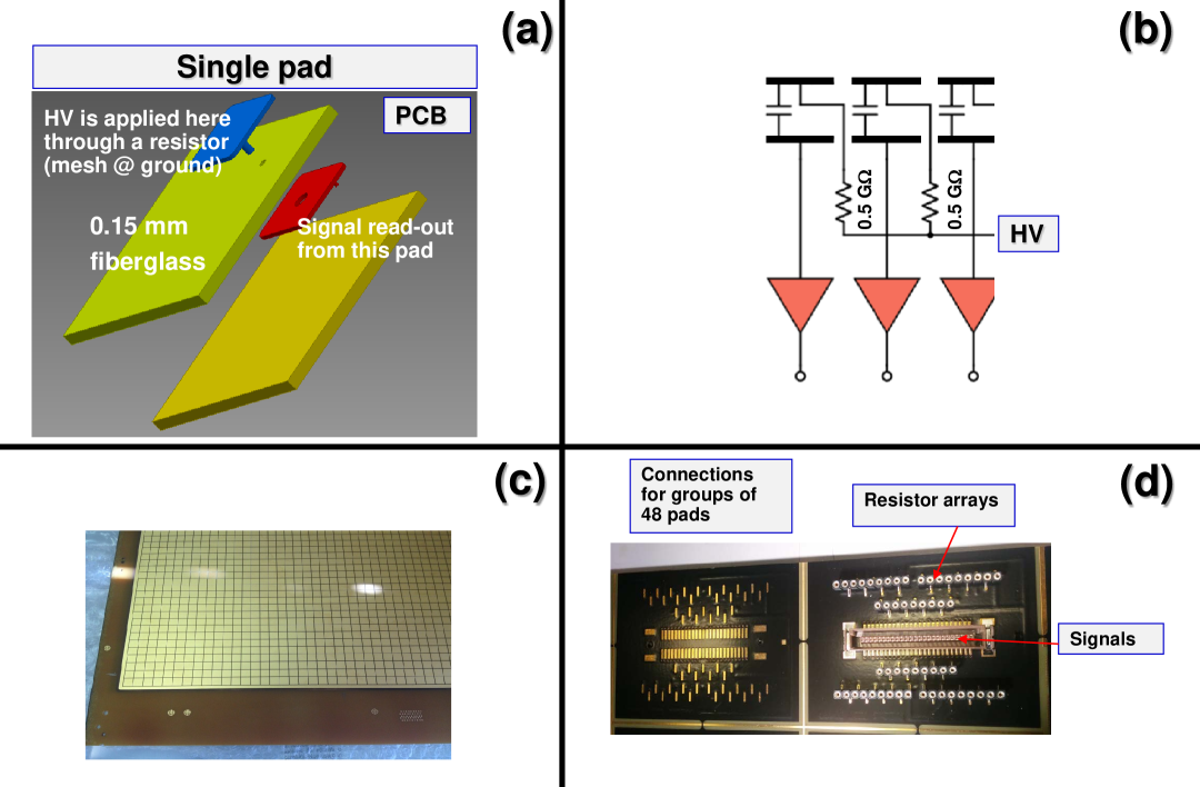
The MM is built with the bulk technology [16]. The resistive MM concept has been adopted and established by an original implementation making use of discrete elements: HV is applied to the anode pads, each one protected by an individual resistor, while the signals are collected from a second set of pads, parallel to the first ones, embedded in the anode PCB, where the signal is transferred by capacitive coupling (Fig. 3). Therefore, in the MM stage, the segmentation of the electrodes is very fine: each single pad acts as an almost independent electrode, thanks to the large-value resistance (470 M) that decouples it from the other pads. The 4760 pads of a detector are supplied by four HV units, each one providing bias to 1190 pads.
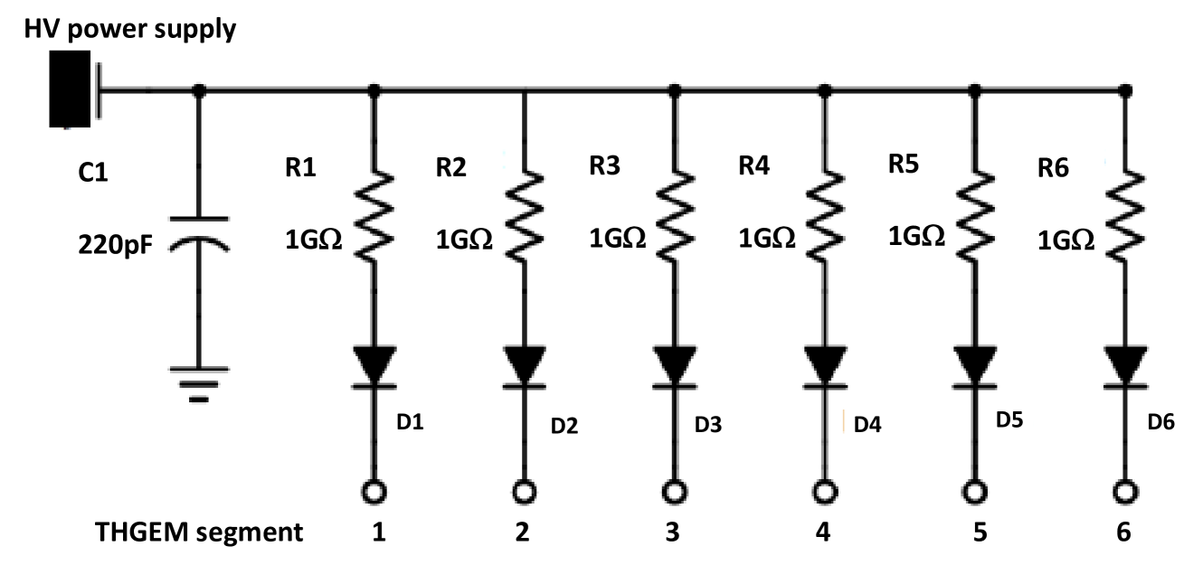
Both surfaces of each THGEM unit (600x300 mm2) are divided into 12 electrodes, referred to as segments in the following. The segments of the top (bottom) THGEM face are grouped by six forming two sectors per THGEM unit, namely four per THGEM plane in a detector. A sector is powered via a single HV channel through a distribution scheme shown in Fig. 4. The segment electrodes are almost independent thanks to the decoupling resistors, while the fast diodes prevent the current flow from a segment to the others in case of an occasional discharge, which acts as a local temporary short. In addition, the THGEM segmentation offers the opportunity to isolate and power independently a few electrically unstable segments.
The detectors are operated with the gas mixture Ar : CH4 = 50 : 50, selected for optimal extraction of the photo-electrons from the converting CsI film to the gaseous atmosphere [7, 8, 9, 10].
The typical voltages applied to the detector electrodes are (with reference to electrodes as indicated in Fig. 1) 1270 V across THGEM1, 1250 V across THGEM2, and 620 V to bias the MM (Tab. 1). The drift field above the first THGEM is 500 V/cm, the transfer field between the two THGEMs is 1000 V/cm and the field between the second THGEM and the MM micromesh is 1000 V/cm. This corresponds to effective gain-values for the three multiplication layers around 12, 10 and 120. These values include electron transfer efficiency.
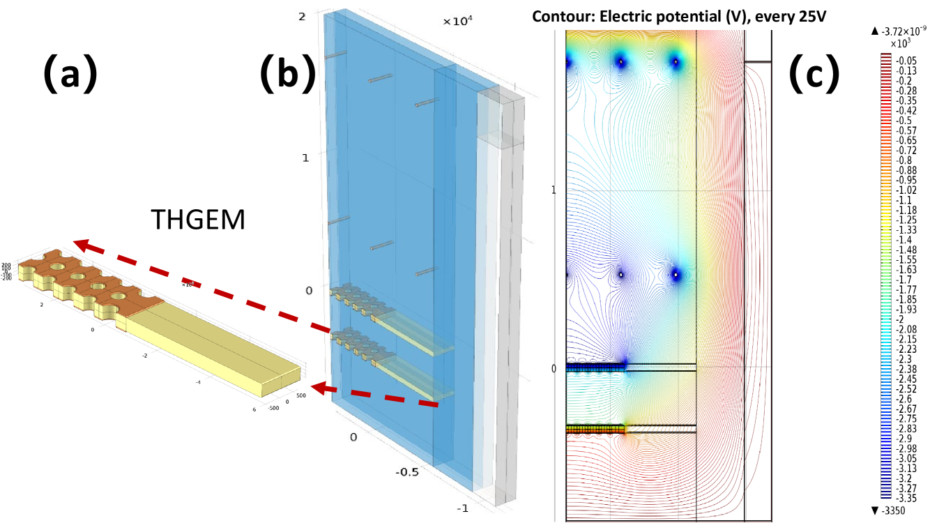
The detector frames are very near to the active surface in order to reduce the dead area between adjacent detectors. These frames are made by aluminum internally covered with an insulator layer of Tufnol 6F/45333by Tufnol Composites Ltd, 76 Wellhead Ln, Birmingham B42 2TN, UK. to prevent discharges from the multiplication electrodes to the frames. Nevertheless, the presence of the frames, obviously properly grounded, can modify the electric field at the detector edges. The calculated electric field maps are shown in Fig. 5; they result in a loss of efficiency and non-stability in the lateral portion of the detectors. The correct electric field configuration is restored by auxiliary electrodes at the lateral sides of the detector frames, embedded below the insulator layers. Two electrodes, biased at different appropriate voltages, are located at each detector lateral edges for a total number of four electrodes per detector.
3 Requirements for the high voltage system
The requirements for the HV system originate from specific requests related to MPGDs in general and from the architecture of the novel detectors (Sec. 2). Current monitoring with fine resolution is needed to control MPGD operation. The multistage structure of the detectors with three transfer and three amplification regions imposes that the main system elements of the HV system are the relative voltages between the cascaded electrodes and not the individual electrodes themselves. Therefore, the applied voltages are highly correlated. Consequently, the control of the voltages is not trivial, while the electrode segmentation adds further elements of complexity. These considerations dictate the first and more important requirement: the automatized control of a complex system in order to prevent errors by the operator.
The complexity of the system also requires to implement automatic protocols to react to occasional misbehaviour of the detectors and to log regularly and at relatively high frequency the relevant parameters, namely the voltages and currents supplied by the HV units.
Changes in pressure and temperature cause gain variations in all gas detectors, which are more severe in multistage detectors because the variations in the amplification stages are combined constructively. Therefore, the HV system has to include sensors to monitor the environmental parameters and protocols to properly modify the applied voltage to compensate for the effect of the parameter variation.
Last, a user-friendly graphical interface is needed to support the operator in controlling the whole system, including about 140 HV power supply channels.
4 The hardware components of the HV system
4.1 The power supply units
Commercial power supply units by CAEN 444CAEN – Costruzioni Apparecchiature Elettroniche Nucleari S.p.A., Via della Vetraia, 11, 55049 Viareggio (Lucca), Italy. are used. We have selected power supplies of the line hosted in the SY4527 mainframe [17], which offers a compact electrical supply to the HV units and the possibility of fast access to the monitoring options via a Gigabit Ethernet interface present in the mainframe control unit. The control of the power supply units is also performed via the same interface.
THGEM electrodes as well as the protection wires, the drift wires and the lateral auxiliary electrodes are powered by A1561HDN 12-channel modules [18] capable of voltage supply down to -6 kV. They are fully floating power supplies, therefore, we can use a very convenient on-detector ground reference, namely the detector frames themselves. The most relevant features of these units for our application are the low voltage ripple, typically 5 mV pp from 10 Hz to 100 MHz at full load, the fine voltage resolution, 100 mV for setting and 10 mV for monitoring, and the fine current resolution, 500 pA for setting the maximum current and 50 pA for monitoring. These figures, which are quoted in the specifications, have been confirmed in operation.
MM pads are supplied by A7030DP 12-channel modules [19], with a maximum voltage of +3 kV. Also these modules are fully floating. The noise figures are 15 mV typical, 20 mV maximum in the range 10-1000 Hz and 5 mV typical, 10 mV maximum above 1000 Hz. The voltage resolution is 50 mV for setting and 10 mV for monitoring. These modules offer less fine current resolution, which is 2 nA for monitoring. A variation of the off-set of the current monitoring has been observed during operation.
The power supply modules are housed in two mainframe SY4527 units, one placed near the top detectors and one placed near the bottom ones to minimize the length of the high voltage cables; with this arrangement, 5 m long cables are used.
4.2 Temperature and pressure measurement system
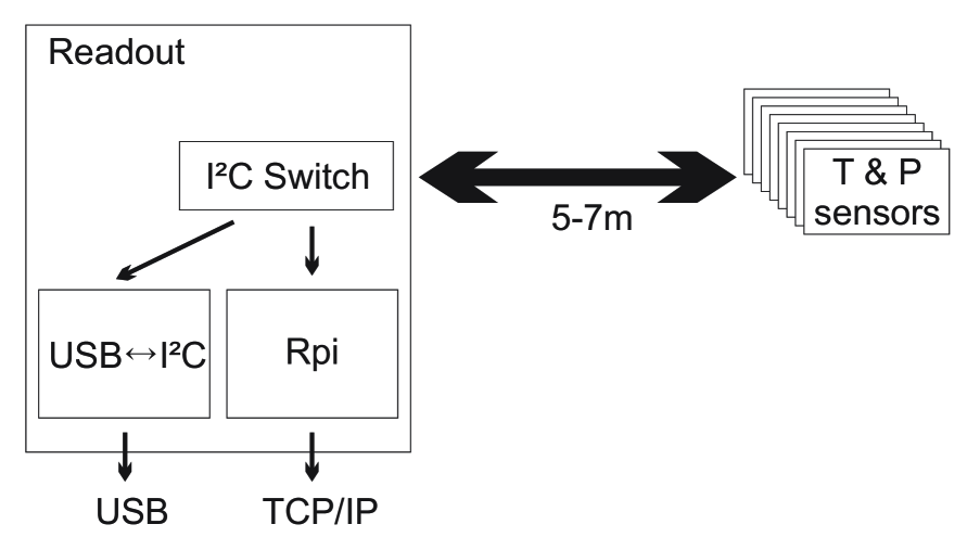
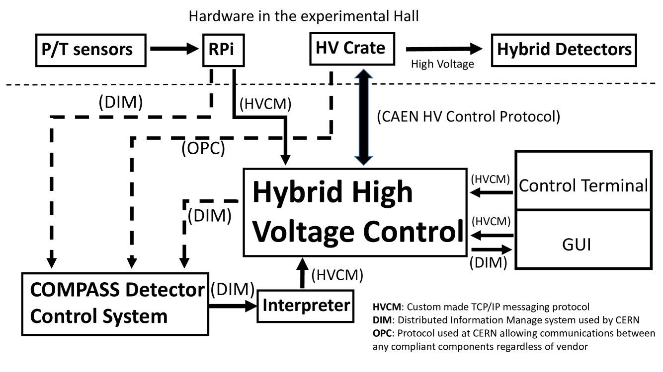
The main components of the system to measure temperature and pressure are the temperature and pressure sensors and the interfaces that make the data available in parallel both to a Single Board Computer (SBC) and to a Linux PC (Fig. 6).
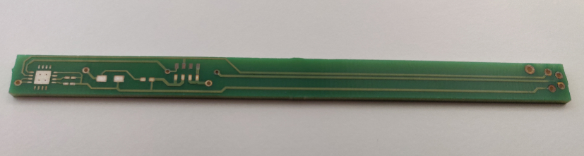
Eight couples of sensors, for temperature and pressure, are used, each mounted on a dedicated board, installed in direct contact with the gas flowing inside the chambers. A reasonably fast following of the temperature changes is obtained by reducing as much as possible the thermal mass of the board. The cable connectors must be gas-tight to avoid gas contamination and leakage. Following these requirements, sensors were mounted on the top of a very narrow PCB (100 mm 7.5 mm), together with an IP67 4-pin M8 connector to allow sensors readout (Fig. 7) . The PCB mechanical support allows direct mounting on the chambers’ frames.
The selected sensor for temperature measurements is the ADT7420 [20] digital sensor by Analog Devices, with 16-bit 0.25∘C accuracy and I2C digital output. The choice for pressure measurements is the MS5611-01BA03 [21] barometric pressure sensor with an accuracy of 2.5 hPa, TE connectivity and an I2C digital output. The choice of these two devices was mainly due to the experience gained during previous developments: they fulfill the requirements on accuracy, stability and robustness.
Eight couples of sensors have to be read, while the sensors themselves have just one or two I2C address bit: it is not possible to mount all the sensors on a single bus. Therefore, multiple I2C buses have been used. They are multiplexed via a Texas Instruments TCA9548A 8-channels I2C switch [22] and each sensor couple is served by an independent I2C bus. The sensor boards are connected to the readout board via 4-cores cables which are up to 7 m-long. The readout frequency is low. Tests and, later, standard operation show that no I2C bus data loss was introduced by the cable length. The TCA9548A switch output is connected both to the Raspberry Pi 3 Model B SBC [23] via its GPIO and to a converter FT232H single channel USB to multipurpose UART/FIFO IC by FTDI [24]. Therefore, it is possible to read out the sensors using the SBC, sending out data via its on-board WiFi, or to read out the data by a computer using its USB connector directly.
In the COMPASS RICH the measured temperature and pressure values are read out locally via the RaspberryPi. The regular readout is followed by a validity check for all the sensors, and if approved are sent to the HV Control System (Sec. 6).
5 Gain calibrations studies
5.1 Gain dependence
In order to understand the gain performance of the hybrid detector, THGEMs and MMs have been extensively characterized by laboratory studies. In general, following the studies by Townsend [25], the gain G has an exponential dependence on the bias voltage applied to a gaseous detector via the first Townsend coefficient:
| (1) |
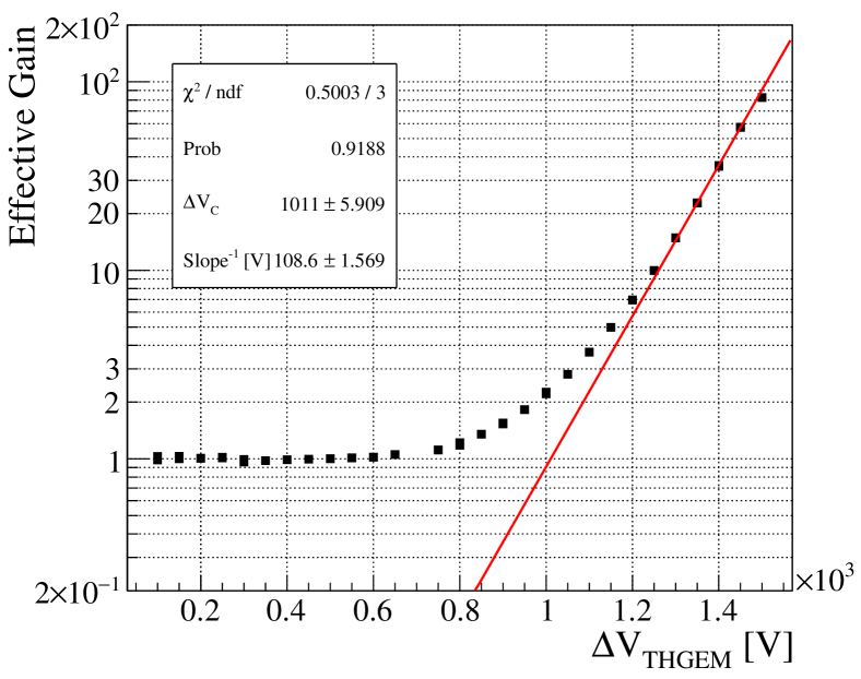
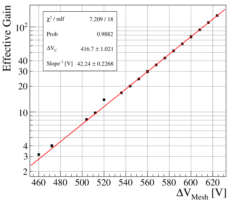
where is the critical voltage where the extrapolated gain is equal to 1. For THGEM with the geometric parameter reported in Sec. 2 and using a gas mixture Ar:CH4 = 50:50, the (Fig. 8), namely, above , an increase of 1 V will result in a 1% gain increase. While for MM with the geometric parameter reported in Sec. 2 and using a gas mixture Ar:CH4 = 50:50, the (Fig. 9), i.e., above , an increase of 1 V will result in a 2% gain increase.
5.2 Gain variation induced by environmental parameters
The dependence of the gain from the environmental parameters, namely temperature and pressure, was studied for the hybrid detector as a whole. This exercise provides useful information only if the three multiplication stages are operated at relative gain-values near to those used in the operation at the experiment, because the slopes of the gain function for THGEMs and MMs are different.
In gaseous detectors, the gain variation due to the environmental parameters is caused by the variation of the gas density, which increases linearly with the pressure P and is inversely proportional to the absolute temperature T. Therefore, considering a limited range of parameter variations, the gain can be regarded as a function of T/P. The function has been determined by laboratory exercises. Measurements performed at fix pressure and varying the temperature, provide interesting indication, but are not fully reproducible. In fact, the temperature of the gas in the detector is a field, which is only partially related to measurements such as the room temperature around the chamber, the temperature of the gas injected in the detector or the gas coming out from it. On the contrary, the gas pressure inside the detector is with very good approximation the same everywhere. Correspondingly, measurements performed at fixed T and varying P provide more reliable information.
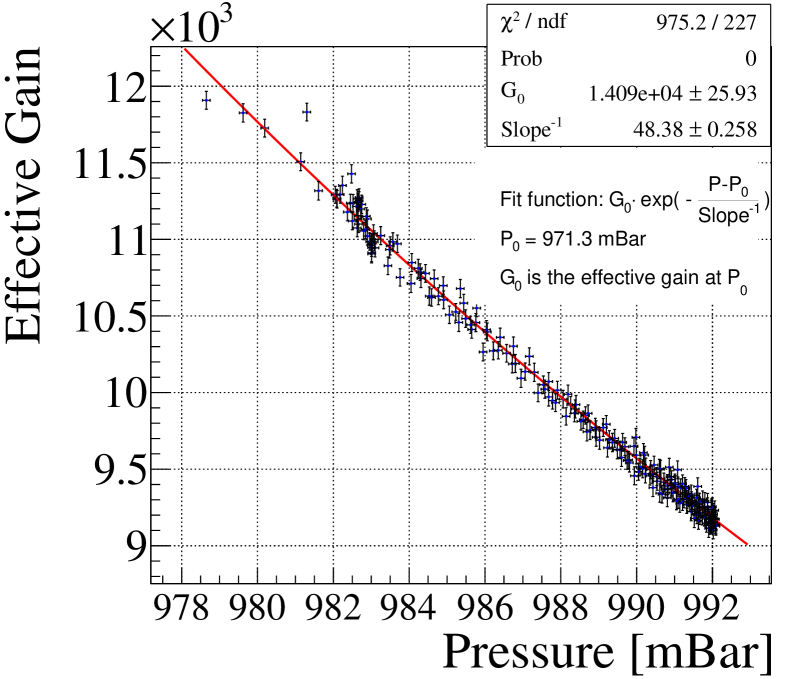
The measurements of the gain dependence versus the gas pressure have been performed illuminating the detector with a 55Fe source; the pressure at the gas-outlet line of the detector was measured with 0.1 mbar resolution; amplitude spectra have been collected. The pressure in the chamber was increased after each gain measurement by increasing the oil level in the safety bubblers downstream of the gas output line. The series of measurements have been performed in a short time interval, so that temperature variations were negligible. Various sets of measurements have been collected at different temperature providing consistent results. The gain evolution versus P is illustrated by one of the sets of measurements shown in Fig. 10: a 10 mbar P variation causes a 20% gain variation. In the measured region, the dependence is approximately linear and its slope can be extracted from the data. The resulting voltage correction algorithm is:
| (2) |
where V is the voltage bias applied to THGEMs or MMs and V0, P0 and T0are fixed reference values. In particular, P0 = 1000 mbar and T0 = 300 K, V0 is the preset voltage for each electrode. In the hybrid detector architecture, the bias voltages of all the three multiplication stages have to be modified to obtain the compensation. Equation 2 provides the correction in term of a voltage correction factor to be applied to the reference voltage setting V0 of each multiplication stage.
The relevance of the compensation is illustrated by two quantitative examples. A temperature variation of 5 K, requires a voltage compensation of about 1% for each multiplication stage, while it would cause a gain variation of 40% if not compensated. Similarly, a pressure variation of 10 mbar can be compensated by a V of 0.5%, while it would cause a gain variation of 20% if not compensated.
There are practical limitations to the effectiveness of the correction procedure. It is difficult to access the gas temperature in a large detector, where the temperature is not homogeneous. We measure the temperature inside the detector volume near to the gas inlet and outlet (Sec. 4.2) and average the two values in order to minimize this effect.
Temperature and pressure values are read out at 1 Hz frequency. Voltage correction is applied every 10 min assuming the average values of temperature and pressure from the last 10 min.
6 The high voltage control
A dedicated High Voltage Control System (HVCS) software package was designed in order to power the COMPASS RICH Hybrids, taking into account the requirements as specified in Sec. 3. In particular, it handles more than hundred HV electrodes, it continuously performs the gain correction required by the modification of the environment parameters, checks the detector’s electrical stability and reacts to the possible detectors misbehaviour, connects to the slow control system of the experiment (named Detector Control System, DCS) and offers the experts control and log of the full detector system.
The schematic block diagram of the whole HV system is shown in Fig. 11, where the communication protocols are highlighted.
The HV power supplies housed in the dedicated HV SY427 crates (Sec. 4.1) are controlled by the Hybrid HV Control (HVC) software package and using the Ethernet port of the crate. HVC addresses the HV channels in the CAEN HV crate using the official CAEN Wrapper libraries. Meanwhile, the monitoring by DCS via the direct access to the crate-resident OPC server is uninterrupted. HVC is written in C/C++ language in order to have low-power, high-performance and high-compatibility.
The communication between the system parts, the DCS, and the users are via messages, using the DIM protocol [26] and a simple TCP/IP socket protocol named “hvcm”, developed at INFN Trieste. Messages are used to send P and T information from the RaspberryPi, placed in the experimental hall. At the same time, messages are used to send information from and to the COMPASS DCS. The actuation by the users and experts is also via messages.
A frequent check and log of voltages and currents are performed at 1 Hz, in order to realize detailed monitoring of the system, in particular of dark currents, and to promptly detect sparks and electrical instabilities. Later, data can be analyzed in details (Sec. 7), while spark-counting is performed on-line. Sparks cause spikes in the current; in case a detector sector sparks at a rate higher than accepted (maximum of 5 sparks per hour), the HVC system automatically decreases its voltage, sends the corresponding information to the DCS, and issues information e-mails to the on-call operator and the experts.
Handling a swarm of channels, several correlated among them, requires a simple and functional scheme. The detector has a well defined ideal voltage setting, assumed as default. The voltages on the real individual sectors and channels are scaled compared to this one. Three scales (multiplication factor) are used, named : SacleSet, ScalePt, and ScaleOwn.
The ScaleSet parameter applies as a general multiplier to all the electrodes of a sector, and is used to access the normal/safe/idle voltage settings, without turning the HV off.
The scaling applied for the required voltage compensation due to a change in environmental parameters are applied via the ScalePt parameter. This multiplier is obviously applied only to the amplification stages (THGEM1, THGEM2, MM).
THGEMs and MMs are not identical due to production limitations and can also be non-uniform. Fine adjustment of the applied voltages of the individual stages helps to achieve a uniform gain throughout the active surface. In case, any electrically feeble segment is present at a particular stage, the sparking probability of that stage can be reduced by decreasing the voltage of that segment. However, the lower voltage reduces the gain of that particular segment. The gain compensation can be made by obtaining a higher gain value at the corresponding segment of a different stage. The fine adjustment of the applied voltage is therefore used to change the gain sharing of the stages for each sector. This fine-tuning of each of the amplification stages is obtained by applying the ScaleOwn parameters.
An excellent gain uniformity has been reached over the segments of the detectors by the fine adjustment of the single amplification stages (Sec. 7.3).
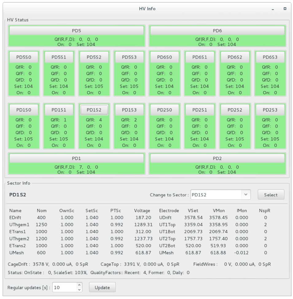
There is no need of interaction from the users during ordinary data taking because everything is automated. On the contrary, during the commissioning phase, a thorough monitoring of the operational parameters and a platform for interactions is needed. A graphical user interface has been written: it reads the parameters of the sectors, including spark counting and actual scales, and shows them in user friendly colour-coded frames that also acts as an interface to set changes of the scales or of the nominal parameters (Fig. 12). The graphical user interface is written in wxWidgeds.
7 Analysis of the high-voltage data
The data logged by HVCS have been analyzed. They include voltages and currents of the different electrodes, as well as temperature and pressure information at the four detectors. The results have been related to the information concerning the detector gain extracted from the COMPASS spectrometer data. In the following, we report the analysis of the data collected during the 2017 COMPASS run, about 80 days long.
7.1 Gain estimation from COMPASS spectrometer data
The behaviour of the detector gain is extracted from the COMPASS spectrometer data. The gain estimation has to rely on a limited-size data sample in order to make possible the assessment of the gain evolution versus time. It also has to be simple and based on RICH data only in order to provide on-line monitoring of the gain evolution.
Sets of one-million events, typically collected in about 5 min, are used. The amplitude spectra of the hits collected in the photon detectors are produced, where the hits are selected according to the criteria reported in the following. The hit readout is performed via the front-end chip APV25 [27]; individual channel pedestal subtraction and thresholding, as well as the subtraction of the common-mode noise, are applied. For hits above the threshold, three amplitudes are measured, namely a2 in-time with the trigger and a1 and a0, respectively, 150 ns and 300 ns before the trigger time. When the measured a2 amplitude is generated by a particle in-time with the event, it is expected that a1 corresponds to a measurement related to the signal rising, while a0 should represent a measurement of the noise level. Therefore, the following condition is imposed to select a hit: 0.2 0.8 and electrons. A typical amplitude spectrum is shown in Fig. 13.
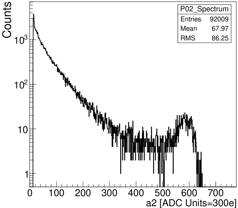
Three regions can be identified in the spectrum: at low amplitudes an important contribution by the residual noise can be observed, at intermediate amplitudes the distribution is dominated by the single Cherenkov photon signals, exponentially distributed, while at larger amplitude the distribution is contributed by the ionization signals due to particles crossing the photon detectors; this last portion of the distribution is also distorted due to the saturation of the dynamic range of the APV25 chip. The intermediate region is used for the estimation, namely the one dominated by the single photon signals, where the amplitude follows with good approximation an exponential distribution.
A gain estimator is used to extract the detector gain. In order to be robust, three algorithms are used. They are all based on the assumption that the distribution is merely due to single photon signals, hence, an exponential distribution. The gain is the reversed of the exponential function slope. The three algorithms are:
-
1.
the gain estimator Gm is calculated from the intermediate region of the distribution in a fixed range (50-200 ADC channels);
-
2.
given a distribution range, the slope can be algebraically calculated; this calculation is repeated for 30 ranges, each of them 150 channel wide, with range starting channel from 40 till 69 and, correspondingly, ending channel from 190 till 219; each calculation provides a value G, with i = 1, 2, …,30; the estimator Gc is the mean value of the 30 G-values;
-
3.
given a distribution range, the slope can be extracted from a two parameter best-fit procedure; this calculation is repeated for 30 ranges, the same used to compute Gc; each calculation provides a value G, with i = 1, 2, …,30; the estimator Gf is the mean value of the 30 G-values.
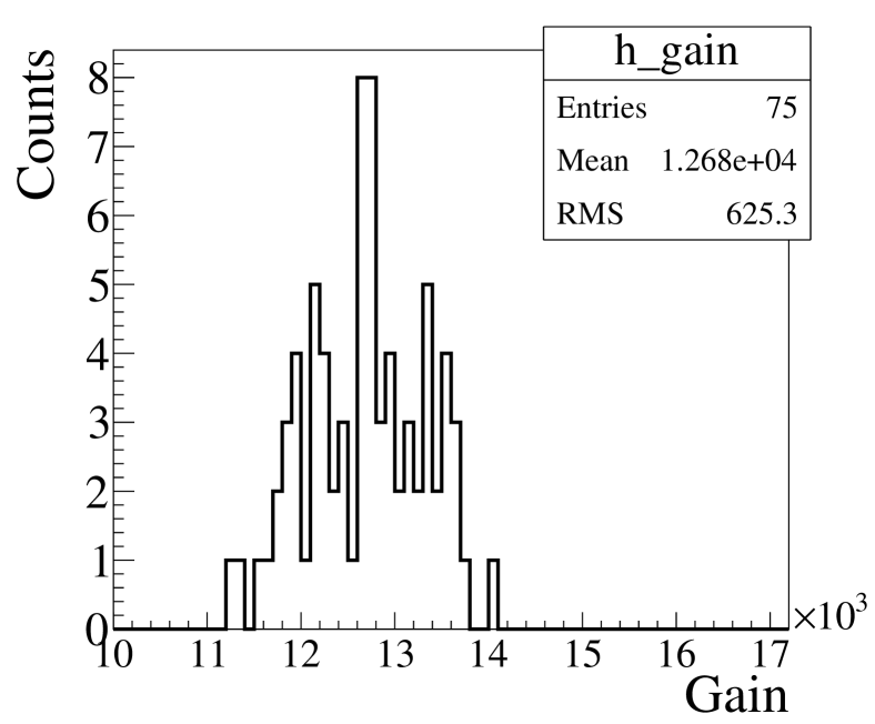
The final gain estimator G=Gf, while Gm and Gc are used to validate the result: Gf is regarded as a valid gain estimation only if the differences between Gf and Gm and between Gf and Gc do not exceed 20%. Its robustness has been assessed as follows: a set of consecutive COMPASS data, around 20 million in total, collected in approximately 1 h, is selected taking care that temperature and pressure variations are negligible and that the photon detectors are stable. It is assumed that the photon detector gain is constant for these data. The data are subdivided into 75 independent subsets of around 250k events and the G-value is extracted for each of them. The results are shown in Fig. 14: the standard deviation of the distribution is less than 5%, proving the robustness of the estimator.
7.2 On-line sparks detection and monitoring
In the hybrid MPGDs installed in RICH-1, sparks result in short current spikes, thanks to the resistive protection applied in the supply schemes of both THGEMs and MMs (Sec. 2).
The power supply parameters reading at 1 Hz makes it possible to know the duration of the spikes and the corresponding restoration time. MM spikes have a duration of 1-2 s, while THGEM spikes last 10 s. The order of magnitude of these recovery times corresponds to the time required for loading the equivalent RC systems. These short duration combined with the very low spike rate of the order of 1/h per detector (Sec. 7.4) and the detector segmentation, which limits the area affected by a spark, makes the dead-time caused by detector sparks totally negligible.
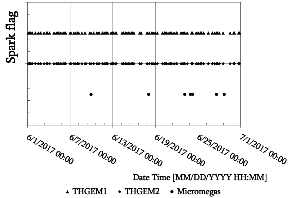
The sparks can be correlated among the different multiplication stages of a detector sector (Fig. 15). Sparks in the two THGEM layers of a sector are 100% correlated. This is expected taking into account that a spark results in a temporary short between the two THGEM electrodes, with a drastic local variation of the electric field that affects also the other THGEM layer. The spark rate in MM is low compared to THGEMs, proving that the implemented resistive MM scheme results in an intrinsically robust multiplication stage. MM sparks are accompanied by sparks in THGEMs in 70% of the cases.
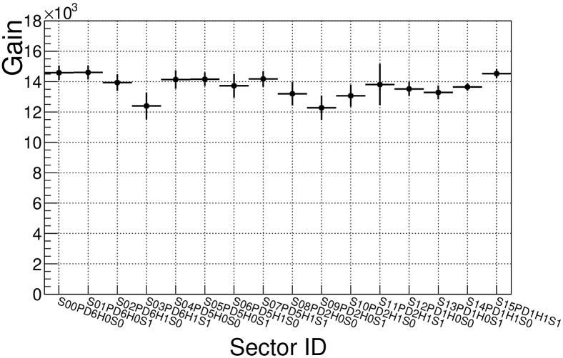
7.3 Gain uniformity
The remarkable gain uniformity obtained with the fine tuning options described in Sec. 6 is shown in Fig. 16, where the gain is estimated with the algorithm described in Sec. 7.1.
7.4 Long-term gain stability
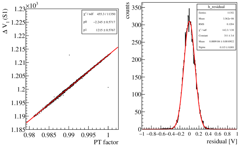
The correct application of the voltage correction is demonstrated by the example in Fig. 17. In Fig. 17, left, where the voltage variation is drawn versus the voltage correction factor for the first THGEM of sector 1 in the photon detector 6. The points of the graph are very well aligned around the fitted straight line. This indicates that the linear correction due to temperature and pressure fluctuations is implemented correctly. The residual between the data points and the linear fit is shown Fig. 17, right. The width of the Gaussian fit indicates that the correction resolution is around 0.1 V, matching the voltage resolution setting of the power supply (Sec. 4.1).
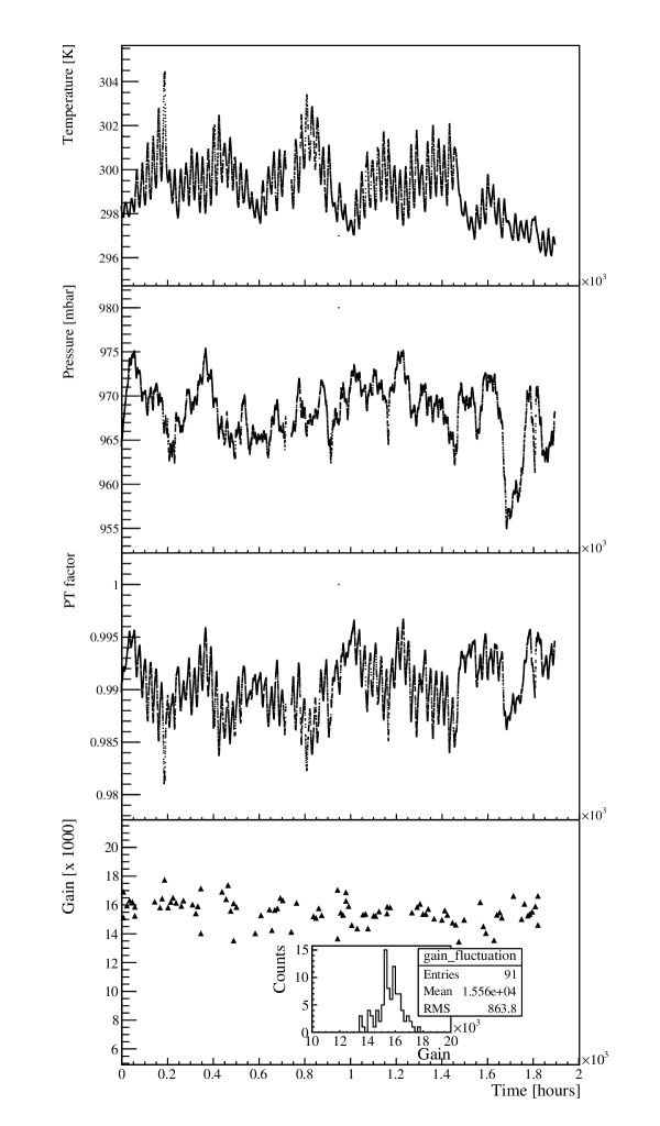
Fig. 18 shows the temperature (first plot from the top) and pressure (second plot from the top) as a function of time for nearly 2000 hours of continuous running. The plotted values are the averaged values of the past 10 min in order to apply voltage corrections. The corresponding voltage correction factor provided by equation 2 is also shown (third plot from the top). The effectiveness of the correction is tested by determining the detector gain from the COMPASS data using the estimator G discussed in Sec. 7.1. Two sets of data per day are used to monitor the gain stability, one collected in the early morning and the other one in the late afternoon, in order to maximize the effect of the daily thermal excursion. As an example, the gain of a sector (PD6 sector 1) is shown in Fig. 18, bottom. The standard deviation of the estimated gain-values is around 6%, which includes the intrinsic fluctuations of the gain estimator. It indicates very good gain stability.
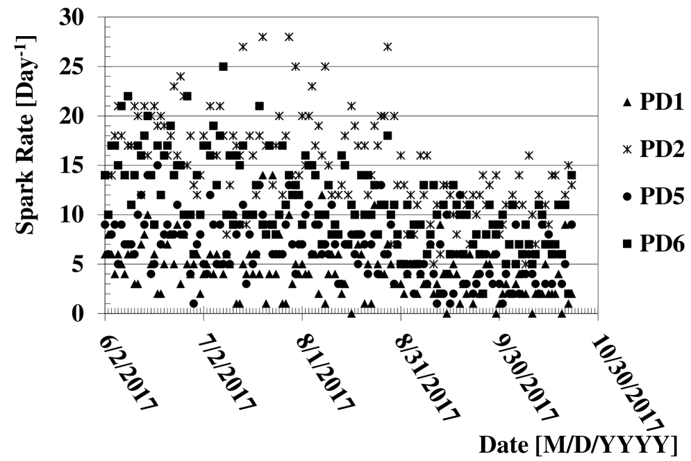
Another evidence of the stability of the whole detector system is the sparks rate in the detector during the physics data taking. Fig. 19 shows the sparks rate for all the sectors of all the four new hybrid detectors from May to October of 2017. Typically, it does not exceed 5/h in total for all four detectors. It could be verified that there is no remarkable dependence on the beam intensity. Sparks correlated in time have been observed for hybrid detectors, also for those sparks happened in sectors which are not contiguous to each other. These observations suggest that a major source of the observed sparks are cosmic rays that occasionally produce relevant ionization in these detectors.
8 Summary
A dedicated HV system with pressure and temperature compensation has been implemented for the MPGD-based photon detectors of COMPASS RICH-1. Its components, namely the commercial power supply, the system for the monitoring of the environmental parameters and the software control system have been described in detail. The overall system fulfills the requirements. The system handles more than hundred HV electrodes, several correlated among them with a fully automatized approach. Voltage corrections able to preserve gain stability in spite of the variation of the environmental parameters are continuously applied and the residual gain variation is at 6% level over months of operation. This system is a central element contributing to the successful use of hybrid MPGD photon detectors in COMPASS RICH-1.
Acknowledgements
The authors are grateful to the colleagues of the COMPASS
Collaboration for continuous support and encouragement.
This work is partially supported by the
H2020 project AIDA-2020, GA no. 654168.
References
References
- [1] E. Albrecht, et al., Status and characterisation of COMPASS RICH-1, Nucl. Instrum. Meth. A553 (2005) 215.
- [2] P. Abbon et al., Design and construction of the fast photon detection system for COMPASS RICH-1, Nucl. Instrum. Meth. A616 (2010) 21.
- [3] P. Abbon et al., Particle identification with COMPASS RICH-1, Nucl. Instr. and Meth. A631 (2011) 26.
- [4] The COMPASS Collaboration, P. Abbon et al., The COMPASS experiment at CERN, Nucl. Instrum. Meth. A577 (3) (2007) 455-518.
- [5] The COMPASS Collaboration, P. Abbon et al., The COMPASS setup for physics with hadron beams, Nucl. Instrum. Meth. A779 (2015) 69.
- [6] J. Agarwala et al., The MPGD-based photon detectors for the upgrade of COMPASS RICH-1 and beyond, Nucl. Instrum. Meth. A 936 (2019) 416.
- [7] M. Alexeev et al., Development of THGEM-based photon detectors for Cherenkov Imaging Counters, 2010 JINST 5 P03009.
- [8] M. Alexeev et al., THGEM-based photon detectors for the upgrade of COMPASS RICH-1, Nucl. Instrum. Meth. A732 (2013) 264.
- [9] M. Alexeev et al., Ion backflow in thick GEM-based detectors of single photons, 2013 JINST 8 P01021.
- [10] M. Alexeev et al., The gain in Thick GEM multipliers and its time-evolution, 2015 JINST 10 P03026.
- [11] L. Periale et al., Detection of the primary scintillation light from dense Ar, Kr and Xe with novel photosensitive gaseous detectors, Nucl. Instrum. Meth. A478 (2002) 377.
- [12] P. Jeanneret, Time Projection Chambers and detection of neutrinos, PhD thesis, Neuchatel University, 2001.
- [13] P.S. Barbeau et al, Toward coherent neutrino detection using low-background micropattern gas detectors IEEE NS-50 (2003) 1285.
- [14] R. Chechik et al, Thick GEM-like hole multipliers: properties and possible applications, Nucl. Instrum. Meth. A535 (2004) 303.
- [15] Y. Giomataris et al., MICROMEGAS: a high-granularity position sensitive gaseous detector for high particle-flux environments, Nucl. Instrum. Meth. A376 (1996) 29.
- [16] I. Giomataris et al., Micromegas in a bulk, Nucl. Instrum. Meth. A560 (2006) 405.
- [17] CAEN, User Manual UM2462 SY4527 - SY4527LC Power Supply Systems, https://www.caen.it/products/sy4527/ .
- [18] CAEN, User Manual A1561H-AG561H 12 Channel 6 kV/20 μA Power Supply Boards, https://www.caen.it/?downloadfile=239 .
- [19] CAEN, User Manual A7030-AG7030 3kV/ 1mA (1.5W) HV Boards, https://www.caen.it/?downloadfile=324 .
- [20] https://www.analog.com/media/en/technical-documentation/data-sheets/adt7420.pdf
- [21] https://www.te.com/usa-en/home.html
- [22] http://www.ti.com/lit/ds/symlink/tca9548a.pdf
- [23] https://www.raspberrypi.org/products/raspberry-pi-3-model-b/
- [24] https://www.ftdichip.com/Support/Documents/DataSheets/ICs/DS_FT232H.pdf
- [25] F. Sauli, Principles of operation of multiwire proportional and drift chambers, CERN 77-09, 3 May 1977.
- [26] Distributed Information Management System, https://dim.web.cern.ch/dim/
- [27] M. J. French et al., Design and results from the APV25, a deep sub-micron CMOS front-end chip for the CMS tracker, Nucl. Instrum. Meth. A466 (2) (2001) 359-365.