Absence of Ferromagnetism in VSe2 Caused by its Charge Density Wave Phase
Abstract
How magnetism emerges in low-dimensional materials such as transition metal dichalcogenides at the monolayer limit is still an open question. Herein, we present a comprehensive study of the magnetic properties of single crystal and monolayer VSe2, both experimentally and ab initio. Magnetometry, X-ray magnetic circular dichrosim (XMCD) and ab initio calculations demonstrate that the charge density wave in bulk stoichiometric VSe2.0 causes a structural distortion with a strong reduction in the density of sates at the Fermi level, prompting the system towards a non-magnetic state but on the verge of a ferromagnetic instability. In the monolayer limit, the structural rearrangement induces a Peierls distortion with the opening of an energy gap at the Fermi level and the absence of magnetic order. Control experiments on defect-induced VSe2-δ single crystals show a breakdown of magnetism, discarding vacancies as a possible origin of magnetic order in VSe2.
I INTRODUCTION
Since the discovery of graphene Novoselov et al. (2004), much scientific effort is concentrated on the characterization of purely two-dimensional (2D) materials. In particular, the family of layered transition metal dichalcogenides (TMDs, MX2: M=Nb, Ti, V,… X= S, Se, Te) is attracting great attention Manzeli et al. (2017); Choi et al. (2017); Zhang and Zhang (2017); Xia et al. (2017) since emergent phenomena driven by novel electronic, optical and quantum many-body properties at the 2D limit could lead to new applications Akinwande et al. (2014). Control over the material thickness down to the monolayer limit has been accurately achieved by mechanical exfoliation Xu et al. (2013), chemical vapor deposition and layer-by-layer Molecular Beam Epitaxy (MBE) Feng et al. (2018); Umemoto et al. (2019), revealing that collective quantum ground states, coherent modulation of electronic periodicities Chen et al. (2018), superconductivity Ugeda et al. (2015), optoelectronic and valley excitonic physics Tran et al. (2019); Seyler et al. (2019); Jin et al. (2019); Alexeev et al. (2019) survive down to the atomic scale.
Nevertheless, long-range magnetic ordering in low dimensions has been elusive for decades. Theoretically, the Mermin-Wagner theorem Mermin and Wagner (1966) prohibits long-range magnetic order in the 2D isotropic Heisenberg model at finite temperatures if the system is spin-rotational invariant. Nevertheless, Ising-type ferromagnetism has been observed in a purely 2D material Huang et al. (2017); Burch et al. (2018); Gibertini et al. (2019), paving the path for future spintronic applications. Moreover, simple defects in a host lattice strongly alter both macroscopic and local properties of the system. Magnetic order from disorder has been observed to emerge in superconducting cuprates upon substitution of non-magnetic ions by spinless impurities Alloul et al. (2009), Kondo systems Praetorius and Fauth (2017) and in highly oriented pyrolytic graphite (HOPG) Červenka et al. (2009), demonstrating that grain boundaries, vacancies and point defects can act as magnetic nuclei in a non-magnetic matrix Yazyev and Helm (2007).
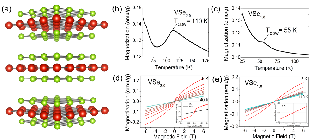
Recently, a strong ferromagnetic (FM) signal at room temperature has been reported at the monolayer limit of the 2D van der Waals system VSe2 Bonilla et al. (2018), broadening the sprectrum of 2D materials hosting magnetism in the ultrathin limit Gong et al. (2017); Guo et al. . van der Waals stacked layers of VSe2 consist of 6-fold coordinated V atoms crystallizing in a trigonal (1T) structure (space group Pm1 in the normal state, NS, see Fig. 1(a)). As many TMDs Bussmann-Holder and Büttner (2002); Wilson et al. (1975), both transport Van Bruggen and Haas (1976); Yadav and Rastogi (2010) and diffraction data Williams et al. (1976) show that bulk VSe2 develops a 3D charge density wave (CDW) below T K Eaglesham et al. (1986) with a new commensurate 4 4 3 lattice periodicity Van Bruggen and Haas (1976); Woolley and Wexler (1977); Strocov et al. (2012). A pseudogap appears at the Fermi surface Bayard and Sienko (1976) and the system remains paramagnetic Van Bruggen and Haas (1976); Bayard and Sienko (1976); Barua et al. (2017a); Cao et al. (2017). Remarkably, TCDW increases at the monolayer limit Xu et al. (2013) and a gap opens at the Fermi level Umemoto et al. (2019) with a controversial magnetic behavior for exfoliated Xu et al. (2013) and MBE-grown monolayers Bonilla et al. (2018). However, a consistent picture about the microscopic origin of magnetism in VSe2 and the development of FM order in this non-magnetic material in 2D is still lacking. In part, this is a consequence of the proximity to electronic and magnetic instabilities which can balance the competition between ground states in the 2D limit. Angle resolved photoemission (ARPES) Chen et al. (2018) and scanning tunneling microscopy (STM) Feng et al. (2018) have revealed an electronic reconstruction of single layer VSe2 compared with the bulk counterpart, without a detectable FM exchange splitting, casting doubts on whether magnetism originates from an induced band structure spin splitting caused by dimensionality reduction or extrinsic defects come into play. Indeed, previous density functional theory (DFT) calculations Li et al. (2014); Ma et al. (2012); Esters et al. (2017); Fuh et al. (2016) found a FM ground state for both bulk and single-layer VSe2. However, these DFT calculations do not take into account the effect of the CDW structure and hence, the electronic reconstruction and the effect of impurities are largely overlooked.
In order to shed light about the nature of the magnetic ground state in VSe2, we have carried out a comprehensive theoretical and experimental study of bulk single crystal and monolayer VSe2. We report that, due to the reduction of the density of states (DOS) at the Fermi level caused by the opening of the CDW pseudo-gap, bulk VSe2 is close to a ferromagnetic instability, which cannot be induced by defects or vacancies. Besides, monolayer VSe2 shows a Peierls-like distortion that opens a gap at the ultrathin limit, preventing the system to develop a long-range FM order, in agreement with recent reports Chen et al. (2018).
II EXPERIMENTAL AND COMPUTATIONAL METHODS
Single crystals of VSe2.0 and VSe1.8 were grown by chemical vapor deposition following previous reports Yadav and Rastogi (2010). 5% excess of Se for VSe2.0 and stoichiometric V:Se (1:2) for VSe1.8 was used during the synthesis. V:Se ratio was measured by Energy-dispersive X-ray spectroscopy (EDX). Single layer VSe2.0 was grown by MBE on epitaxial bilayer graphene on Silicon carbide (Si-C) and highly oriented pyrolytic graphite (HOPG) substrates in an ultrahigh vacuum chamber with a base pressure of 110-9 and 250∘C. After the growth, three minutes post-annealing in Se-rich atmosphere was carried out to fill in the Se vacancies. A Se capping layer was deposited after cooling to prevent oxidation and was in situ evaporated for XMCD experiments. Magnetic measurements on Se-capped VSe2 monolayers grown on diamagnetic bilayer graphene/SiC were carried out in a SQUID magnetometer up to 7 Tesla. X-ray magnetic circular dichroism (XMCD) at the V L2,3-edge up to 6 T was performed at the BOREAS beamline at ALBA synchrotron Barla et al. (2016). Normal and grazing incidence geometries are referred to to 90º and 20º angle between the beam and sample surface, the latter being more sensitive to in-plane magnetization, and the magnetic field is always parallel to the beam direction. Cluster calculations were carried out using crystal field theory implemented in the QUANTY code Haverkort et al. (2012); Lu et al. (2014) for the atomic-like 2p6 - 3dδ 2p5-3dδ+1 transitions. First principles DFT ab initio electronic structure calculations Hohenberg and Kohn (1964); Kohn and Sham (1965) were performed using an all-electron full potential code (wien2k Schwarz and Blaha (2003)). The exchange-correlation term for the bulk structure was the generalized gradient approximation (GGA) in the Perdew-Burke-Ernzerhof Perdew et al. (1996) scheme. The LDA+U method was used for the 2D case Anisimov et al. (1997). The calculations were carried out with a converged k-mesh and a value of RmtKmax= 7.0 and a Rmt value of 2.12 a. u. for both V and Se. Transport properties were obtained with the BoltzTrap2 code Madsen et al. (2018) using a denser k-mesh, solving the Boltzmann transport equation within the constant scattering time approximation.
III RESULTS
The paper is organized as follows: first, we present the experimental and theoretical results obtained for bulk VSe2, followed by showing the results for the system at the monolayer limit.
III.1 Bulk VSe2
Plotted in Fig. 1 (b-c) are the temperature dependence of the magnetization for VSe2.0 and VSe1.8 single crystals. Following previous reports Van Bruggen and Haas (1976); Yadav and Rastogi (2010), the CDW transition is identified as a kink in the magnetic susceptibility; at 110 K for VSe2.0 and 55 K for VSe1.8, evidencing the drop in transition temperature upon introducing Se defects. Interestingly, the field dependence of the magnetization shows s-shape magnetic behavior for VSe2.0 (Fig. 1d and inset) but absent in single crystals of VSe1.8 (Fig. 1e). Nevertheless, neither the magnetization of VSe2.0 nor VSe1.8 saturates at 6 T. The small magnetic behavior observed in VSe2.0 could arise from Kondo impurities Barua et al. (2017b) or phase slippage of the CDW Grüner (1994).
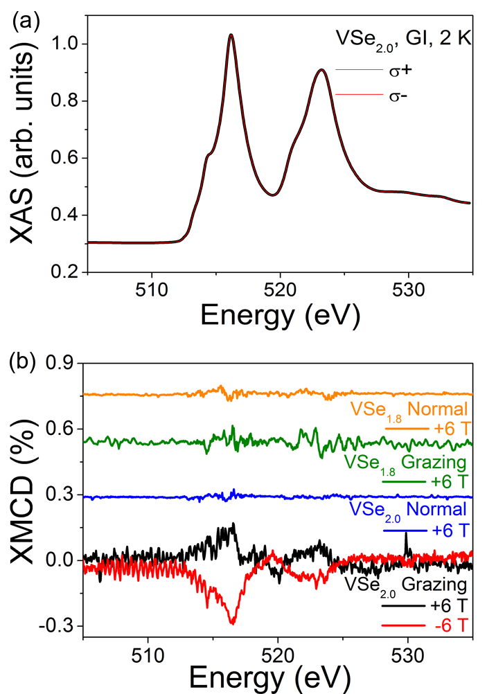
To identify the source of magnetism in VSe2.0 single crystals, we have carried out X-ray magnetic circular dichroism (XMCD) at the V L2,3 edge at 6 T (Fig. 2). As shown in Fig. 2(b), a small XMCD signal, defined as (+--), can only be detected in VSe2.0 at the L2,3 in grazing incidence geometry (GI) at 6 T, suggesting that small moments are in-plane aligned. On the other hand, no significant dichroic signal is detected in VSe1.8 for normal and grazing incidence geometries. Comprehensive transport data highlighted the Kondo effect in VSe2.0 single crystals below 40 K Barua et al. (2017b), thus, the small magnetic dichroism at the V L2,3 edge can be assigned to Kondo impurities. Nevertheless, the small XMCD signal precludes us to retrieve a hysteresis loop from the magnetic dichroism experiments. Further, the introduction of Se vacancies seems to be detrimental to magnetism.
In order to obtain a deep understanding of the electronic and magnetic ordering in single crystals of VSe2.0, we have carried out ab initio calculations, both in the normal (NS) and CDW state. ARPES and X-ray diffraction Van Bruggen and Haas (1976) have found a 3-dimensional CDW below 110 K, leading to the opening of a pseudo-gap at the Fermi level at (, , ) reciprocal lattice units Terashima et al. (2003). To take this into account in our calculations, we have computed a 4 4 3 supercell. Therefore, the introduction of a periodic lattice distortion may affect the calculated DOS at the Fermi level and hence the magnetic properties of this itinerant electron system.
Since VSe2 is an itinerant-electron system, one can make use of the phenomenological Stoner model Stoner (1938) to analyze how close the system is to a magnetic instability. The Stoner theory compares the energy gained by the system via a spin splitting to the kinetic energy cost produced by displacing minority-spin electrons into a higher-energy majority-spin band. Only when the overall energy gets reduced, an itinerant electron system becomes spontaneously magnetic. The Stoner criterion states that the system will be FM if and non-magnetic otherwise, where is the exchange energy between the Bloch d-band electrons, the so called Stoner parameter Moriya (1985). Itinerant ferromagnets such as Fe, Ni and Co present values of ranging from 2.5 to 3 Fritsche and Weimert .
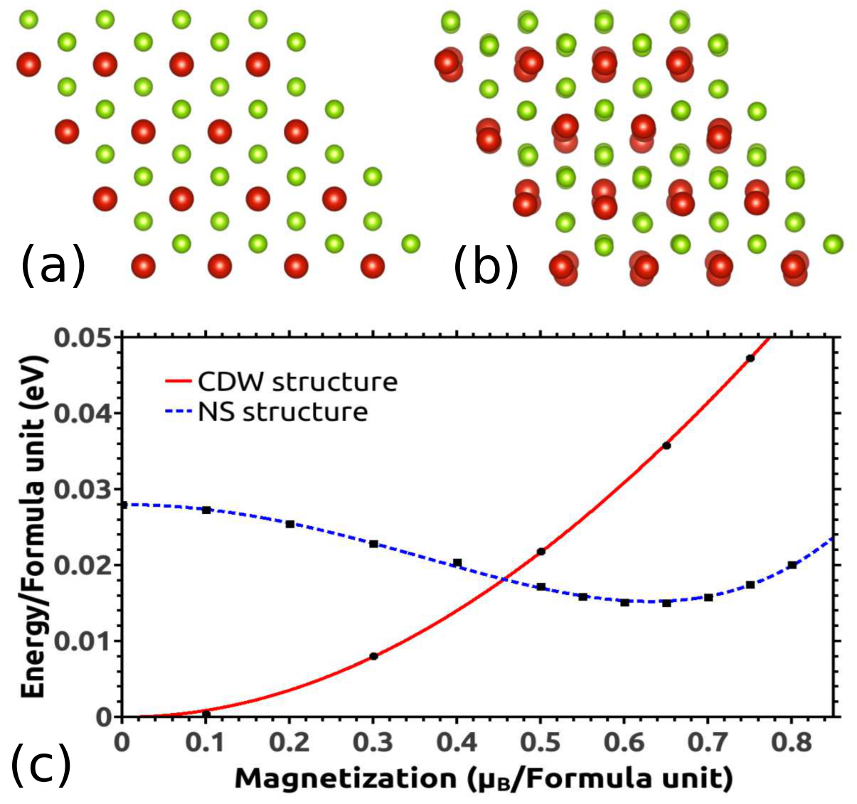
It follows from the energy (E) vs magnetization (M) curve that the bulk normal state yields a FM ground state with a broad minimum around at per V atom, (blue line in Fig. 3c), with and is a fitting parameter independent of Moriya (1985). The Fermi level is located at , where n is the number of electrons per formula unit and () implies hole (electron) doping, and the carrier concentration was calculated using a rigid-band approximation by integrating the total DOS of the non-magnetic calculation. In Fig. 4a, we show that the Stoner criterion for FM is satisfied for -0.5n0.5. However, any perturbation to this system leads to a small reduction in the DOS at the Fermi level and to a non-magnetic state. Previous ab initio studies have shown that a reduction of the FM moment can be achieved by strain engineering Ma et al. (2012). Very recently, W. Zhang et al. Zhang et al. (2019) took advantage of the proximity of VSe2 to a magnetic ground state to engineer a FM heterostructure of VSe2 with a magnetic moment of about 0.4 per V atom, as we have predicted here. This finding highlights that monolayers of VSe2 can be manipulated to tailor new magnetic ground states.
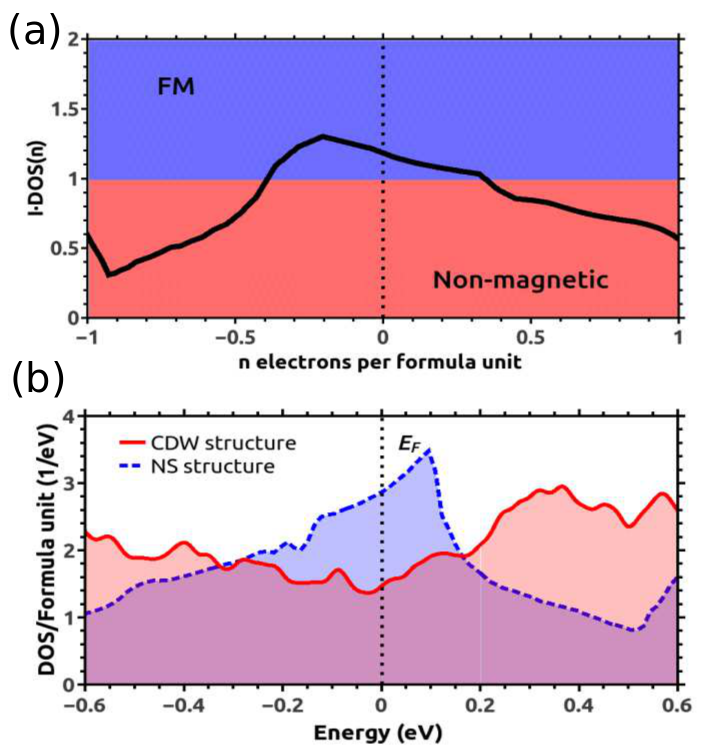
The optimized atomic positions at low temperature (CDW state), taking into account the new lattice periodicity Van Bruggen and Haas (1976), are plotted in Fig. 3b, showing that the short-range hexagonal symmetry is lost. The CDW structure calculated ab-initio is per formula unit more stable than the NS structure resulting in a strong reduction of the DOS at the Fermi level (Fig. 4b) and a quenching of the FM moment as compared with the NS (Fig. 3c).
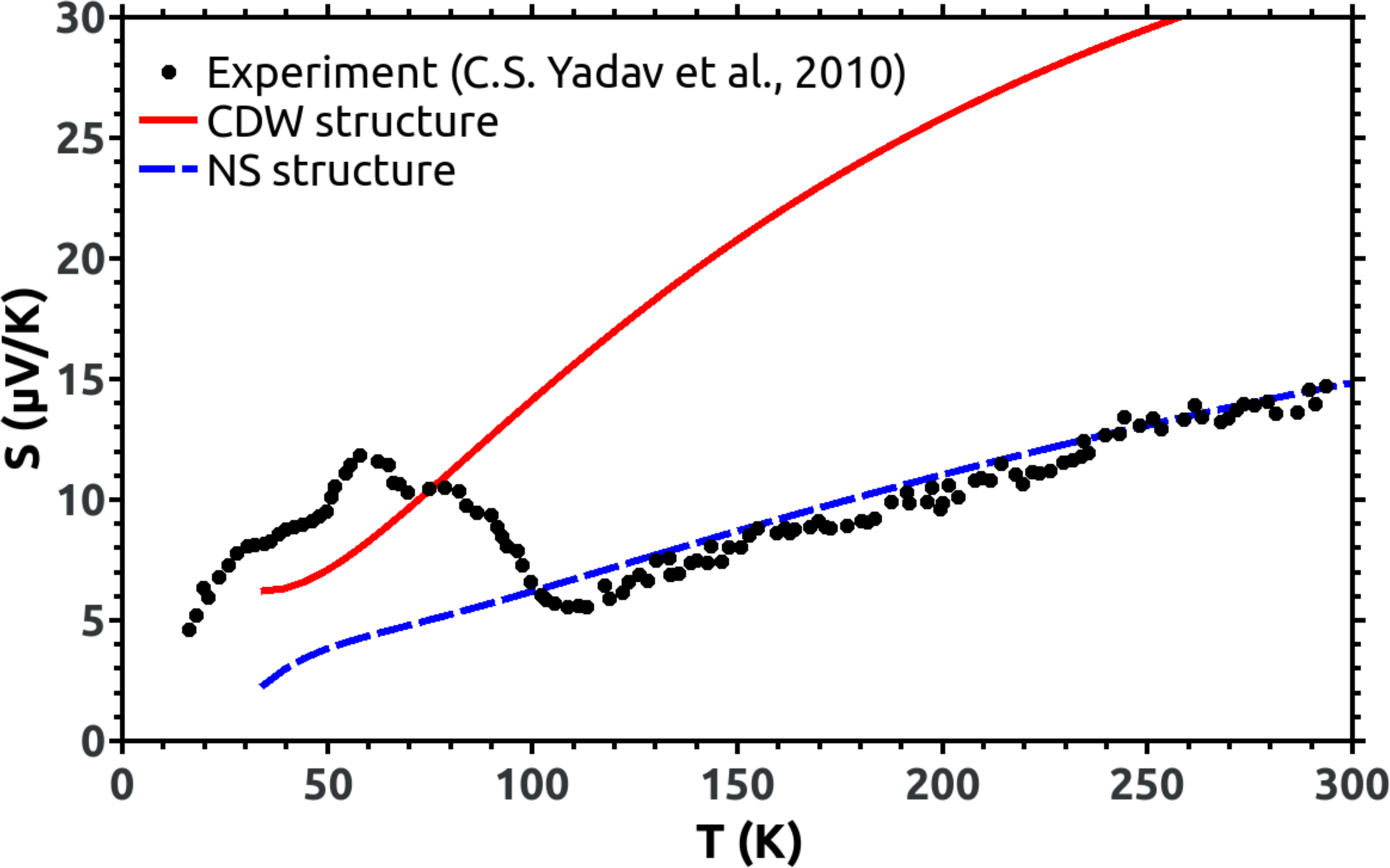
Experimentally, a significant enhancement in the Seebeck effect is observed at the transition from the NS at high temperatures to the CDW state below 110 K, due to the opening of a pseudo-gap at the Fermi level. In Fig. 5 the computed thermopower of both the NS (blue dashed line) and the CDW (red line) structures is compared to the ones in the literature Yadav and Rastogi (2010) (black points), evidencing that the relaxed structure can be modeled reasonably well with the CDW state found experimentally. Despite the coarse fitting at low temperature, an enhancement of the thermopower with respect to the NS is also obtained in the theoretical simulations within the constant scattering time approximation. This is further evidence for the reliability of modelling bulk VSe2 in its CDW phase using a 4 4 3 supercell.
III.2 Monolayer VSe2
Figure 6(a-b) shows the atomic force microscopy (AFM) image of high quality monolayer VSe2.0 grown on HOPG and Si-C, respectively, with typical heights of 6 Å. The field dependence of the magnetization (M[H]) at 300 and 5 K for VSe2.0 grown on Si-C substrate is presented in Figure 6(c). The magnetic curves show a negative slope characteristic of the diamagnetic signal from the Si-C substrate, without indications of saturation or hysteresis, ruling out any magnetism coming from the VSe2.0 monolayers, at least within the limit of detection of our setup. This is confirmed in 6(d) after the subtraction of the magnetic signal of the Si-C substrate. Besides, XMCD at 6 T shows a featureless magnetic dichroism in normal or grazing incidence, as shown in Fig. 6(f). Here, we point out that similar magnetic dichroism has been recently reported for spin frustrated monolayers of VSe2Wong et al. (2019). In addition, a careful comparison between the XAS spectra of the single crystals and the monolayer also reveals a broadening of the L3 edge in the ultra-thin limit, presumably as a consequence of the electronic reconstruction in the 2D limit.
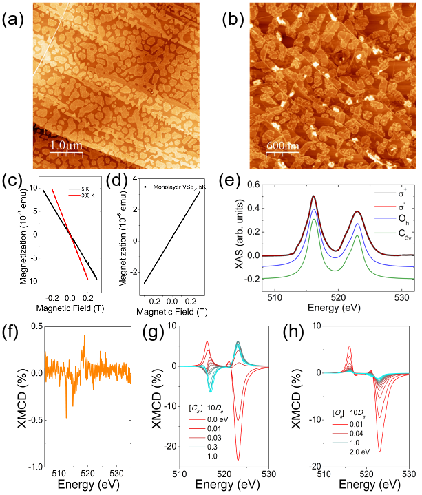
To estimate the theoretical dichroism expected for a d1 system, we have carried out cluster calculations in the octahedral and trigonal crystal field for the atomic-like 3d transitions using QUANTY. The code incorporates the intra-atomic 3d-3d and 2p-3d, magnetic exchange interactions, the atomic 2p and 3d spin-orbit couplings and local crystal field parameter and Coulomb energies (Slater integrals) obtained within the Hartree-Fock approximation Haverkort (2005).
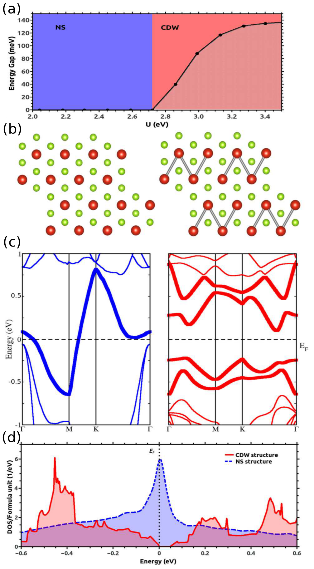
Figure 6f and 6(g-h) show the experimental and the simulated isotropic spectrum, defined as ++- as a function of the crystal field 10Dq expected for spin- in a trigonal and octahedral symmetries. To simulate the monolayer VSe2 spectra, we used 40% of the atomic values of the Slater integrals in the Oh and C3v symmetries of the V sites. As shown in Fig. 6 (g-h), the crystal field calculations for spin- V4+ reveal a finite, but crystal-field dependent, 10Dq, magnetic dichroism. Strain effects induced by the HOPG and SiC-graphene, which might alter the crystal field parameter, are found to be negligible in 2D monolayer TMDs. Therefore, the absence of magnetic dichroism in single layer VSe2.0 points to a strong electronic renormalization at the ultrathin limit. In fact, screening effects are enhanced with respect to the bulk VSe2.0, thus leading to an additional renormalization of the DOS. Indeed, the CDW phase is observed at T T Xu et al. (2013), revealing an enhancement of the electron-electron and electron-phonon interactions in 2D. Furthermore, the hopping parameter, t, between layers vanishes and, hence, the ratio between the on-site Coulomb repulsion and hopping, Ut, increases.
Following ARPES experiments Feng et al. (2018); Chen et al. (2018); Coelho et al. (2019), the ground state of monolayer VSe2 is characterized by an energy gap. However, the electronic modulation of the CDW remains under discussion Feng et al. (2018); Umemoto et al. (2019); Chen et al. (2018). Therefore, our aim within the following DFT calculations will be to explain the physical mechanism that undergoes the monolayer rather than looking for perfect agreement with controversial experimental data. We present calculations on a 2 2 supercell since it was computationally affordable. This will allow us to understand the possible electronic reconstructions that may occur in the 2D limit when a periodic lattice distortion takes place, shedding light on how both the FM quenching and the full-gap opening occur. In order to include the electron interactions that become stronger in the monolayer limit, we have performed LDA+U calculations. Figure 7(a) shows the evolution of the energy gap in the whole Brillouin zone as a function of U for a fully relaxed 2 2 supercell of the monolayer. At reduced values of U, a metallic FM structure is stable. However, for U greater than eV a non-magnetic CDW is formed and, consequently, an energy gap appears in the whole Brillouin zone, in agreement with experiments Chen et al. (2018). The calculated band structures for the non-magnetic-monolayer NS and CDW state are shown in Fig. 7(c). If no structural instability is present, the d-band crossing at the Fermi level and the high density of states (blue dashed line in Fig. 7(d)) lead to a FM metallic state. Nevertheless, the structural transition associated to the CDW, depicted in Fig. 7(b), drives the system towards a Peierls-like distortion with a tetramerization among 4 V atoms. A comparison between the DOS of the NS structures both for the bulk and the monolayer reveals that decreasing dimensionality increases the DOS at the Fermi level, the bands become flatter due to the absence of the off-plane hopping. In general, for itinerant systems, this would be a mechanism to enhance the stability of a FM phase. However, due to the CDW state, the 4 d-bands in the 2 2 supercell hybridize forming 2 bonding and 2 antibonding bands (right side of Fig. 7(b) opening an energy gap (red line in Fig. 7(d)) with a concomitant quenching of the FM moment.
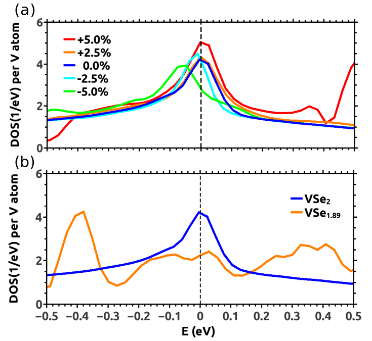
Finally, in order to study ab initio the intrinsic effect of strain and Se vacancies in the monolayer limit, we have computed the DOS for different strain values and also carried out similar calculations including Se vacancies in a V:Se ratio similar to our single-crystal experiments (Fig. 8). We have performed calculations in the NS and shown that the DOS is not substantially increased (mostly reduced) with respect to the unstrained-stoichiometric NS monolayer VSe2.0. The effect of strain and Se vacancies can be seen in Fig. 8(a-b), suggesting that neither strain nor Se vacancies will induce an intrinsic FM state in single-layer VSe2.0, as discussed above in our experiments for the bulk case.
IV DISCUSSION AND CONCLUSIONS
Recently, transport and magnetometry experiments have reported a FM ground state for monolayers of VSe2 grown on different substrates Bonilla et al. (2018). This is in agreement with previous DFT calculations that have predicted the emergence of a FM ground state for monolayers of VX2 (X=S, Se) Li et al. (2014); Ma et al. (2012); Esters et al. (2017); Fuh et al. (2016). Our combination of experimental data, including magnetization and XMCD, find a small ferromagnetic signal for stoichiometric bulk VSe2.0, which may arise from V impurities intercalated in the van der Waals gap. Naively, one may think that this Kondo mechanism gets inoperative when reducing the dimensionality of VSe2.0 down to the ultrathin limit, since no van der Waals gap is present. Nonetheless, still impurities in the surface of the monolayer can produce a Kondo effect. In the bulk case, ab initio calculations show that a CDW phase of the periodicity found experimentally destroys magnetism and is the ground state structure. Recently, first principles calculations of the CDW structure of monolayer VSe2 also reported a distorted CDW structure more stable than the FM one, indicating a competition of magnetism and CDW Coelho et al. (2019).
Following our XMCD data and DFT calculations, we have found a non-magnetic ground state in monolayer VSe2, in agreement with recent ARPES data Feng et al. (2018); Chen et al. (2018) that demonstrates the absence of spin-polarized bands in the monolayer limit Chen et al. (2018). More recent work Wong et al. (2019) also reports a non-magnetic but frustrated ground state in monolayer VSe2 due to a competition between ferro and antiferromagnetic orders. In addition, defects are shown to be detrimental to ferromagnetism, unlike the emergence of the vacancy-induced magnetism observed in graphite Červenka et al. (2009). Although our magnetization data does not allow us to reveal a frustrated magnetic ground state, the absence of long range magnetic order due to disorder and vacancies corroborates such magnetic frustration. Nevertheless, despite our DFT calculations find a drop of DOS at the Fermi level discarding a possible FM state, the effect of intrinsic disorder in monolayer VSe2 has to be carefully studied experimentally, since high density of vacancies, anti-sites, substitutions, edges and grain boundaries can dominate the materialsfl properties.
In conclusion, we have studied experimentally and theoretically the ground state of bulk and monolayers of VSe2. Our DFT calculations predict that the ground state of bulk VSe2 develops a commensurate lattice distortion with a 4 4 3 supercell that reproduces the variation of the thermopower at high and low temperature, demonstrating the importance of considering the correct ground state structure when performing ab initio studies in magnetic materials. This structure is shown to be related with the CDW phase that has been experimentally detected at low temperatures. Our DFT calculations for such a ground state show that FM is destroyed by such distortion, VSe2 being a paramagnet in the bulk but on the verge to a magnetic state. This result confirms previous analysis that highlight the importance of phonon instabilities, besides electronic ones, in driving the formation of the CDW state Johannes and Mazin (2008). It also reconciles theory and experiment. In the monolayer limit, we found that a periodic lattice distortion (2 2) associated to the CDW state is sufficient to open an energy gap through a Peierls-like distortion destroying the tendency towards a FM state, as we have reported experimentally by means of magnetization and XMCD. Our calculations suggest that the origin of the magnetic signal obtained for VSe2.0 cannot be related to the band structure of the material, either in the bulk or in the single-layer limit and any magnetic ground state in the monolayer limit might be associated to a high density of defects, edges or grain boundaries, although control experiments in bulk VSe1.8 and ab initio calculations in single layer VSe2.0 indicate that strain induced by vacancies work against ferromagnetism in clear contrast to the magnetic ground state recently reported in few layer PtSe2 Avsar et al. (2019), presumably due to the strong competition between ferro- and antiferromagnetic states Wong et al. (2019).
V Acknowledgements
This work is supported by the MINECO of Spain through the project MAT2016-80762-R, PGC2018-101334-A-C22 and PGC2018-101334-B-C21. A.O.F. thanks MECD for the financial support received through the FPU grant FPU16/02572. M.G. acknowledges funding from the European Commission through the Marie Sklodowska-Curie IEF project SUPER2D (GA-748971). M.M.U. acknowledges support by the Spanish MINECO under grant no. MAT2017-82074-ERC and by the ERC Starting grant “LINKSPM” (Grant 758558). A. Berger and L. H. Hueso are acknowledged for sharing CIC nanoGUNE facilities and the SQUID measurements. S.B-C thanks IKERBASQUE for financial support. We also thank J. Fernández-Rossier, I. Oleynik, Warren E. Pickett and D. Soriano for fruitful discussions and ALBA Synchrotron Light Facility for the provision of synchrotron beamtime.
References
- Novoselov et al. (2004) K. S. Novoselov, A. K. Geim, S. V. Morozov, D. Jiang, Y. Zhang, S. V. Dubonos, I. V. Grigorieva, and A. A. Firsov, Science 306, 666 (2004), http://science.sciencemag.org/content/306/5696/666.full.pdf .
- Manzeli et al. (2017) S. Manzeli, D. Ovchinnikov, D. Pasquier, O. V. Yazyev, and A. Kis, Nature Reviews Materials 2, 17033 (2017).
- Choi et al. (2017) W. Choi, N. Choudhary, G. H. Han, J. Park, D. Akinwande, and Y. H. Lee, Materials Today 20, 116 (2017).
- Zhang and Zhang (2017) G. Zhang and Y.-W. Zhang, J. Mater. Chem. C 5, 7684 (2017).
- Xia et al. (2017) J. Xia, J. Yan, and Z. X. Shen, FlatChem 4, 1 (2017).
- Akinwande et al. (2014) D. Akinwande, N. Petrone, and J. Hone, Nature Communications 5, 5678 EP (2014), review Article.
- Xu et al. (2013) K. Xu, P. Chen, X. Li, C. Wu, Y. Guo, J. Zhao, X. Wu, and Y. Xie, Angewandte Chemie International Edition 52, 10477 (2013).
- Feng et al. (2018) J. Feng, D. Biswas, A. Rajan, M. D. Watson, F. Mazzola, O. J. Clark, K. Underwood, I. Marković, M. McLaren, A. Hunter, D. M. Burn, L. B. Duffy, S. Barua, G. Balakrishnan, F. Bertran, P. Le Fèvre, T. K. Kim, G. van der Laan, T. Hesjedal, P. Wahl, and P. D. C. King, Nano Letters 18, 4493 (2018), pMID: 29912565.
- Umemoto et al. (2019) Y. Umemoto, K. Sugawara, Y. Nakata, T. Takahashi, and T. Sato, Nano Research 12, 165 (2019).
- Chen et al. (2018) P. Chen, W. W. Pai, Y.-H. Chan, V. Madhavan, M. Y. Chou, S.-K. Mo, A.-V. Fedorov, and T.-C. Chiang, Phys. Rev. Lett. 121, 196402 (2018).
- Ugeda et al. (2015) M. M. Ugeda, A. J. Bradley, Y. Zhang, S. Onishi, Y. Chen, W. Ruan, C. Ojeda-Aristizabal, H. Ryu, M. T. Edmonds, H.-Z. Tsai, A. Riss, S.-K. Mo, D. Lee, A. Zettl, Z. Hussain, Z.-X. Shen, and M. F. Crommie, Nature Physics 12, 92 EP (2015), article.
- Tran et al. (2019) K. Tran, G. Moody, F. Wu, X. Lu, J. Choi, K. Kim, A. Rai, D. A. Sanchez, J. Quan, A. Singh, J. Embley, A. Zepeda, M. Campbell, T. Autry, T. Taniguchi, K. Watanabe, N. Lu, S. K. Banerjee, K. L. Silverman, S. Kim, E. Tutuc, L. Yang, A. H. MacDonald, and X. Li, Nature 567, 71 (2019).
- Seyler et al. (2019) K. L. Seyler, P. Rivera, H. Yu, N. P. Wilson, E. L. Ray, D. G. Mandrus, J. Yan, W. Yao, and X. Xu, Nature 567, 66 (2019).
- Jin et al. (2019) C. Jin, E. C. Regan, A. Yan, M. Iqbal Bakti Utama, D. Wang, S. Zhao, Y. Qin, S. Yang, Z. Zheng, S. Shi, K. Watanabe, T. Taniguchi, S. Tongay, A. Zettl, and F. Wang, Nature 567, 76 (2019).
- Alexeev et al. (2019) E. M. Alexeev, D. A. Ruiz-Tijerina, M. Danovich, M. J. Hamer, D. J. Terry, P. K. Nayak, S. Ahn, S. Pak, J. Lee, J. I. Sohn, M. R. Molas, M. Koperski, K. Watanabe, T. Taniguchi, K. S. Novoselov, R. V. Gorbachev, H. S. Shin, V. I. Fal’ko, and A. I. Tartakovskii, Nature 567, 81 (2019).
- Mermin and Wagner (1966) N. D. Mermin and H. Wagner, Phys. Rev. Lett. 17, 1133 (1966).
- Huang et al. (2017) B. Huang, G. Clark, E. Navarro-Moratalla, D. R. Klein, R. Cheng, K. L. Seyler, D. Zhong, E. Schmidgall, M. A. McGuire, D. H. Cobden, W. Yao, D. Xiao, P. Jarillo-Herrero, and X. Xu, Nature 546, 270 (2017).
- Burch et al. (2018) K. S. Burch, D. Mandrus, and J.-G. Park, Nature 563, 47 (2018).
- Gibertini et al. (2019) M. Gibertini, M. Koperski, A. F. Morpurgo, and K. S. Novoselov, Nature Nanotechnology 14, 408 (2019).
- Alloul et al. (2009) H. Alloul, J. Bobroff, M. Gabay, and P. J. Hirschfeld, Rev. Mod. Phys. 81, 45 (2009).
- Praetorius and Fauth (2017) C. Praetorius and K. Fauth, Phys. Rev. B 95, 115113 (2017).
- Červenka et al. (2009) J. Červenka, M. Katsnelson, and C. Flipse, Nature Physics 5, 840 (2009).
- Yazyev and Helm (2007) O. V. Yazyev and L. Helm, Phys. Rev. B 75, 125408 (2007).
- Bonilla et al. (2018) M. Bonilla, S. Kolekar, Y. Ma, H. C. Diaz, V. Kalappattil, R. Das, T. Eggers, H. R. Gutierrez, M.-H. Phan, and M. Batzill, Nature Nanotechnology (2018), 10.1038/s41565-018-0063-9.
- Gong et al. (2017) C. Gong, L. Li, Z. Li, H. Ji, A. Stern, Y. Xia, T. Cao, W. Bao, C. Wang, Y. Wang, Z. Qiu, R. Cava, S. G. Louie, J. Xia, and X. Zhang, , JTh5C.2 (2017).
- (26) Y. Guo, H. Deng, X. Sun, X. Li, J. Zhao, J. Wu, W. Chu, S. Zhang, H. Pan, X. Zheng, X. Wu, C. Jin, C. Wu, and Y. Xie, Advanced Materials 29, 1700715.
- Bussmann-Holder and Büttner (2002) A. Bussmann-Holder and H. Büttner, Journal of Physics: Condensed Matter 14, 7973 (2002).
- Wilson et al. (1975) J. Wilson, F. D. Salvo, and S. Mahajan, Advances in Physics 24, 117 (1975), https://doi.org/10.1080/00018737500101391 .
- Van Bruggen and Haas (1976) C. F. Van Bruggen and C. Haas, Solid State Communications 20, 251 (1976).
- Yadav and Rastogi (2010) C. Yadav and A. Rastogi, Solid State Communications 150, 648 (2010).
- Williams et al. (1976) P. M. Williams, C. B. Scruby, W. B. Clark, and G. S. Parry, Le Journal de Physique Colloques 37, C4 (1976).
- Eaglesham et al. (1986) D. J. Eaglesham, R. L. Withers, and D. M. Bird, Journal of Physics C: Solid State Physics 19, 359 (1986).
- Woolley and Wexler (1977) A. M. Woolley and G. Wexler, Journal of Physics C: Solid State Physics 10, 2601 (1977).
- Strocov et al. (2012) V. N. Strocov, M. Shi, M. Kobayashi, C. Monney, X. Wang, J. Krempasky, T. Schmitt, L. Patthey, H. Berger, and P. Blaha, Phys. Rev. Lett. 109, 086401 (2012).
- Bayard and Sienko (1976) M. Bayard and M. Sienko, Journal of Solid State Chemistry 19, 325 (1976).
- Barua et al. (2017a) S. Barua, M. C. Hatnean, M. R. Lees, and G. Balakrishnan, Scientific Reports 7 (2017a), 10.1038/s41598-017-11247-4.
- Cao et al. (2017) Q. Cao, F. F. Yun, L. Sang, F. Xiang, G. Liu, and X. Wang, Nanotechnology 28, 475703 (2017).
- Li et al. (2014) F. Li, K. Tu, and Z. Chen, The Journal of Physical Chemistry C 118, 21264 (2014).
- Ma et al. (2012) Y. Ma, Y. Dai, M. Guo, C. Niu, Y. Zhu, and B. Huang, ACS Nano 6, 1695 (2012).
- Esters et al. (2017) M. Esters, R. G. Hennig, and D. C. Johnson, Phys. Rev. B 96, 235147 (2017).
- Fuh et al. (2016) H.-R. Fuh, B. Yan, S.-C. Wu, C. Felser, and C.-R. Chang, New Journal of Physics 18, 113038 (2016).
- Barla et al. (2016) A. Barla, J. Nicolás, D. Cocco, S. M. Valvidares, J. Herrero-Martín, P. Gargiani, J. Moldes, C. Ruget, E. Pellegrin, and S. Ferrer, Journal of Synchrotron Radiation 23, 1507 (2016).
- Haverkort et al. (2012) M. W. Haverkort, M. Zwierzycki, and O. K. Andersen, Phys. Rev. B 85, 165113 (2012).
- Lu et al. (2014) Y. Lu, M. Höppner, O. Gunnarsson, and M. W. Haverkort, Phys. Rev. B 90, 085102 (2014).
- Hohenberg and Kohn (1964) P. Hohenberg and W. Kohn, Phys. Rev. 136, B864 (1964).
- Kohn and Sham (1965) W. Kohn and L. J. Sham, Phys. Rev. 140, A1133 (1965).
- Schwarz and Blaha (2003) K. Schwarz and P. Blaha, Comp. Mater. Sci. 28, 259 (2003).
- Perdew et al. (1996) J. P. Perdew, K. Burke, and M. Ernzerhof, Phys. Rev. Lett. 77, 3865 (1996).
- Anisimov et al. (1997) V. I. Anisimov, F. Aryasetiawan, and A. I. Lichtenstein, J. Phys.: Condens. Mat. 9, 767 (1997).
- Madsen et al. (2018) G. K. Madsen, J. Carrete, and M. J. Verstraete, Computer Physics Communications 231, 140 (2018).
- Barua et al. (2017b) S. Barua, M. C. Hatnean, M. R. Lees, and G. Balakrishnan, Scientific Reports 7, 10964 (2017b).
- Grüner (1994) G. Grüner, Charge Density Waves in Solids (Addison-Wesley, 1994).
- Terashima et al. (2003) K. Terashima, T. Sato, H. Komatsu, T. Takahashi, N. Maeda, and K. Hayashi, Physical Review B 68 (2003), 10.1103/PhysRevB.68.155108.
- Stoner (1938) E. C. Stoner, Proceedings of the Royal Society of London A: Mathematical, Physical and Engineering Sciences 165, 372 (1938).
- Moriya (1985) T. Moriya, Spin fluctuations in itinerant electron magnetism, Springer Series in Solid-State Sciences (Springer-Verlag, 1985).
- (56) L. Fritsche and B. Weimert, physica status solidi (b) 208, 287.
- Zhang et al. (2019) W. Zhang, L. Zhang, P. K. J. Wong, J. Yuan, G. Vinai, P. Torelli, G. van der Laan, Y. P. Feng, and A. T. S. Wee, ACS Nano (2019), 10.1021/acsnano.9b02996.
- Wong et al. (2019) P. K. J. Wong, W. Zhang, F. Bussolotti, X. Yin, T. S. Herng, L. Zhang, Y. L. Huang, G. Vinai, S. Krishnamurthi, D. W. Bukhvalov, Y. J. Zheng, R. Chua, A. T. N’Diaye, S. A. Morton, C.-Y. Yang, K.-H. Ou Yang, P. Torelli, W. Chen, K. E. J. Goh, J. Ding, M.-T. Lin, G. Brocks, M. P. de Jong, A. H. Castro Neto, and A. T. S. Wee, Advanced Materials 31, 1901185 (2019), https://onlinelibrary.wiley.com/doi/pdf/10.1002/adma.201901185 .
- Haverkort (2005) M. Haverkort, Spin and orbital degrees of freedom in transition metal oxides and oxide thin films studied by soft x-ray absorption spectroscopy, Ph.D. thesis, Universität zu Köln (2005).
- Coelho et al. (2019) P. M. Coelho, K. Nguyen Cong, M. Bonilla, S. Kolekar, M.-H. Phan, J. Avila, M. C. Asensio, I. I. Oleynik, and M. Batzill, The Journal of Physical Chemistry C 123, 14089 (2019).
- Johannes and Mazin (2008) M. D. Johannes and I. I. Mazin, Phys. Rev. B 77, 165135 (2008).
- Avsar et al. (2019) A. Avsar, A. Ciarrocchi, M. Pizzochero, D. Unuchek, O. V. Yazyev, and A. Kis, Nature Nanotechnology 14, 674 (2019).