Large spin-relaxation anisotropy in bilayer-graphene/WS heterostructures
Abstract
We study spin-transport in bilayer-graphene (BLG), spin-orbit coupled to a tungsten di sulfide (WS) substrate, and measure a record spin lifetime anisotropy 40-70, i.e. ratio between the out-of-plane and in-plane spin relaxation time . We control the injection and detection of in-plane and out-of-plane spins via the shape-anisotropy of the ferromagnetic electrodes. We estimate 1-2 ns via Hanle measurements at high perpendicular magnetic fields and via a new tool we develop: Oblique Spin Valve measurements. Using Hanle spin-precession experiments we find a low 30 ps in the electron-doped regime which only weakly depends on the carrier density in the BLG and conductivity of the underlying WS, indicating proximity-induced spin-orbit coupling (SOC) in the BLG. Such high and spin lifetime anisotropy are clear signatures of strong spin-valley coupling for out-of-plane spins in BLG/WS systems in the presence of SOC, and unlock the potential of BLG/transition metal dichalcogenide heterostructures for developing future spintronic applications.
Graphene (Gr) in contact with a transition metal dichalcogenide (TMD), having high intrinsic spin-orbit coupling (SOC) offers a unique platform where the charge transport properties in Gr are well preserved due to the weak van der Waals interaction between the two materials. However, the spin transport properties are greatly affected due to the TMD-proximity induced SOC in graphene Wang et al. (2016); Gmitra and Fabian (2015); Omar and van Wees (2018). At the Gr/TMD interface, the spatial inversion symmetry is broken, and the graphene sublattices having K(K’) valleys experience different crystal potentials and spin-orbit coupling magnitudes from the underlying TMD. The electron-spin degree of freedom and its interaction with other properties such as valley pseudospins in the presence of SOC provide access to spintronic phenomena such as spin-valley coupling Xiao et al. (2007); Leutenantsmeyer et al. (2018); Xu et al. (2018); Zihlmann et al. (2018); Cummings et al. (2017); Ghiasi et al. (2017), spin-Hall effect Safeer et al. (2019); Garcia et al. (2017), (inverse) Rashba-Edelstein effect Song et al. (2017); Soumyanarayanan et al. (2016); Isasa et al. (2016); Sánchez et al. (2013); Shen et al. (2014) and even topologically protected spin-states Kane and Mele (2005); Yang et al. (2016); Frank et al. (2018); Du et al. (2018); Island et al. (2019) which are not possible to realize in pristine graphene. The mentioned effects are sought after for realizing enhancement and electric field control of SOC Khoo et al. (2017); Gmitra and Fabian (2017); Afzal et al. (2018); Ye et al. (2017); Wang et al. (2016); Omar and van Wees (2018, 2017), efficient charge-current to spin-current conversion and vice versa Safeer et al. (2019); Offidani et al. (2017); Huang et al. (2017); Ando and Shiraishi (2016), which will be the building blocks for developing novel spintronic applications Soumyanarayanan et al. (2016); Gurram et al. (2018).
Experiments on Gr/TMD systems confirm the presence of enhanced spin-orbit coupling Omar and van Wees (2018); Wang et al. (2015) and the anisotropy in the in-plane () and out-of-plane () spin relaxation times Ghiasi et al. (2017); Benítez et al. (2018); Zihlmann et al. (2018) in single layer graphene. Recent theoretical studies Khoo et al. (2017); Gmitra and Fabian (2017) predict that due to the special band-structure of bilayer-graphene on a TMD substrate, it is expected to show a larger spin-relaxation anisotropy even up to 10000 Gmitra and Fabian (2017), which is approximately 1000 times higher than the highest reported values for single-layer graphene-TMD heterostructures Ghiasi et al. (2017); Zhu and Kawakami (2018). As explained in Ref. Gmitra and Fabian (2017), a finite band-gap opens up in bilayer-graphene (BLG) in presence of a built-in electric field at the BLG/TMD interface, which can be tuned via an external electric field. The BLG valence (conduction) band is formed via the carbon atom orbitals at the bottom (top) layer. As a consequence, due to the closer proximity of the bottom BLG layer with the TMD, the BLG valence band has almost two order higher magnitude of SOC of spin-valley coupling character than the SOC in the conduction band. This modulation in the SOC can be accessed in two ways: either by the application of a back-gate voltage by tuning the Fermi energy or via the electric-field by changing the sign of the orbital-gap. Depending on whether the graphene is hole or electron doped, and the magnitude of the electric field at the interface, BLG can therefore exhibit the effect of spin-valley coupling in the magnitude of spin-relaxation anisotropy ratio .
In this letter, we report the transport of both in-plane and out-of-plane spins in BLG supported on a TMD substrate, i.e. tungsten disulfide (WS2). We inject and detect the out-of-plane spins in graphene via a purely electrical method by exploiting the magnetic shape anisotropy of the ferromagnetic electrodes at high magnetic fields Tombros et al. (2008); Popinciuc et al. (2009); Guimarães et al. (2014), in contrast with the optical injection of out-of-plane spins into Gr/TMD systems in refs. Avsar et al. (2017); Luo et al. (2017). We extract 1 ns-2 ns, which results in 40-70 via two independent methods; Hanle measurements at high perpendicular magnetic field and a newly developed tool Oblique Spin Valve measurements. Such large confirms the existence of strong spin-valley coupling for the out-of-plane spins in BLG/TMD systems. We find a weak modulation in both and as a function of charge carrier density in the electron-doped regime in the BLG. varies from 15-30 ps, with such short values indicating the presence of a very strong spin-orbit coupling in the BLG, induced by the WS2 substrate.
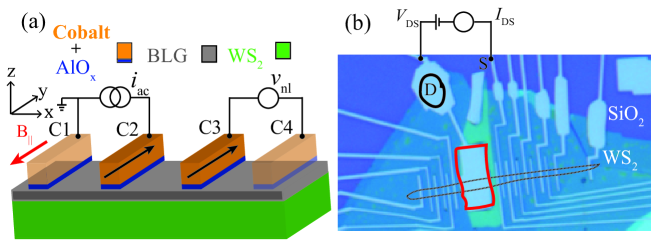
Bilayer-graphene/WS2 samples are prepared on a SiO2/Si substrate (thickness 500 nm) via a dry pick-up transfer method Zomer et al. (2014) (see Supplemental Material for fabrication details).
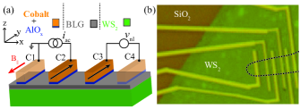
We study two bottom-WS/BLG samples (thickness 3 nm), labeled as stack A and stack B, and present the data from the left region of stack A (Fig. 1(b)) as a representative sample. Additional measurements from stack B and the right-side region of stack A are presented in Supplemental Material, also show similar results. We use a low-frequency ac lock-in detection method to measure the charge and spin transport properties of the graphene flake. In order to measure the I-V behavior of the bottom WS2 flake and for gate-voltage application, a Keithley 2410 dc voltage source was used. All measurements are performed at Helium temperature (4 K) under vacuum conditions in a cryostat.
Details of charge and spin-transport measurement methods and TMD characterization are provided in Supplemental Material. We obtain the BLG electron-mobility 3,000 cm2V-1s-1, which is somewhat low compared to the previously reported mobility values in graphene on a TMD substrate Omar and van Wees (2018); Wang et al. (2016).
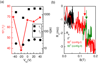
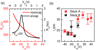
We perform spin-transport measurements, using the measurement scheme shown in Fig. 1(a) and measure the nonlocal signal . For in-plane spin transport, the spin-signal is defined as =, where is the measured for the (anti-)parallel magnetization orientations of the injector-detector electrodes. From non-local spin-valve (SV) and Hanle spin-precession measurements, we obtain the spin diffusion coefficient and in-plane spin-relaxation time , and estimate the spin-relaxation length = . A representative Hanle measurement for stack A is shown in Fig. 2(b). Due to small magnitudes of in-plane spin-signals and invasive ferromagnetic (FM) contacts ( 1k), we were able to get information about the in-plane spins via Hanle measurements only for short injector-detector separation of about 1-2 m. Since we could not access the hole-doped regime for the applied back-gate voltage due to heavily n-doped samples, we only measure the spin-transport in the electron-doped regime for both stacks. For stack A, we obtain 0.01 m2s-1 and in the range 18-34 ps, i.e. 0.45-0.54 m. For stack B, we obtain 0.03 m2s-1 and in the range 17-24 ps, i.e. 0.6-0.7 m. In conclusion, though for both samples we obtain reasonable charge transport properties, i.e. 0.01 m2s-1, we obtain a very low down to 16 ps. The weak modulation of with the back-gate voltage suggests a strong SOC induced in the BLG in contact with WS Wang et al. (2016) and the insignificant contribution of the spin-absorption mechanism for the applied back-gate voltage range in contrast with the behavior observed in refs. Yan et al. (2016); Dankert and Dash (2017); Benítez et al. (2018).
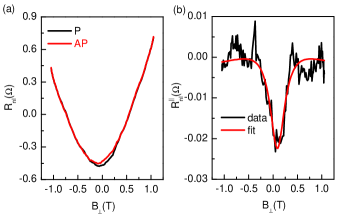
In order to explore the proposed spin-relaxation anisotropy in BLG/WS systems Gmitra and Fabian (2017), we inject out-of-plane spins electrically by controlling the magnetization direction of the FM electrodes via an external magnetic field. Due to its finite shape anisotropy along the z-axis, the magnetization of the FM electrode does not stay in the device plane at high enough . For the FM electrodes with the thickness 65 nm, their magnetization can be aligned fully in the out-of-plane direction at 1.5 T Tombros et al. (2008); Leutenantsmeyer et al. (2018). At 0.3 T, the magnetization makes an angle 10∘ with the easy-axis of the FM electrode, which increases with the field (see Supplemental Material for details). In this case, the injected spins, along with the dephasing in-plane spin-signal component as shown in Fig. 2(b) also have a non-precessing out-of-plane spin-signal component, which would increase with due to the contact magnetization aligning towards (Fig. 2(a)). From this measurement, we can estimate by removing the contribution of the in-plane spin-signal and the background charge (magneto)resistance, i.e. (for details, refer to Supplemental Material) and fit with the following equation:
| (1) |
Here is the measured signal for out-of-plane spins for the injector-detector separation , channel width , with out-of-plane spin relaxation length . is the graphene sheet resistance at T. We assume that both electrodes have equal spin-injection and detection polarization , which we obtain in the range 3-5 via regular in-plane spin-transport measurements (see Supplemental Material for details).
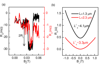
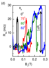
BLG on TMD is expected to have Gmitra and Fabian (2017), which also implies that at , i.e. will be higher in magnitude than at . In our measurements, this effect reflects as a strong increase in at high for both P and AP configurations (Fig. 2(a)). Via charge magnetoresistance measurements (see Supplemental Material) for the same channel, we confirm that the observed enhancement in is not due to the magnetoresistance originating from the orbital effects under the applied out-of-plane magnetic field. Next, we show the distance dependence of in Fig. 3. The in-plane spin signal is reduced almost by factor of ten from 10 m to 1 m (Fig. 3(a)). On the other hand, for the same distance decreases roughly by less than factor of three. From this measurement, we confirm that in the BLG/WS heterostructures. We fit the experimental data in Fig. 3(b) with Eq. 1 for different , and obtain 3.3 m-4.1 m. We extract from the relation , while we assume equal for in-plane and out-of-plane spins Benítez et al. (2018), and obtain 1 ns-1.6 ns, resulting in a large anisotropy 50-70.
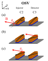
In order to confirm the spin life-time anisotropy in BLG/WS system and to accurately measure the out-of-plane spin-signals even in the possible presence of a background charge-signal, we develop a new tool; Oblique Spin-Valve (OSV) measurements. For the OSV measurements, we follow a similar measurement procedure as in the SV measurements. However, for the magnetization reversal of FM electrodes, we apply a magnetic field which makes an angle with their easy-axes in the y-z plane as shown in Fig. S9(a), instead of applying in SV measurements in Fig. 1(a). As a result, the magnetization of the FM electrodes also makes a finite angle with its easy axis. In this way, we inject and detect both in-plane and out-of-plane spins in the spin-transport channel. The in-plane magnetic field is responsible for the magnetization switching of C2 and C3 (see details in Supplemental Material). At the event of magnetization reversal at a magnetic field in the OSV measurements, the spin-signal change would appear as a sharp switch in . However, the magnetic field dependent background signal does not change. In this way, in the OSV measurements, we combine the advantages of both SV and the perpendicular-field Hanle measurements, and obtain background-free pure spin-signals.
In an OSV measurement, we measure fractions of both and . The OSV spin-signal consists of two components: an in-plane spin-signal component proportional to and an out-of-plane spin-signal component proportional to which get dephased by the applied magnetic field and , respectively:
| (2) |
where is the functional form for the in-plane (out-of-plane) spin precession dynamics. At larger , the dephasing of in-plane spin-signal is enhanced. Conversely, the dephasing of out-of-plane spin-signal is suppressed. Also, increases with . Therefore, at higher is dominated by and acquires a similar form as in Eq. 1.
Due to the expected spin-life time anisotropy in BLG/TMD systems and as observed in Hanle measurements in Fig. 3(b), the out-of-plane spin signal magnitude increases with the magnetization angle . Similar effect would appear in the OSV measurements at larger values due to fact that the magnetization switching would occur at larger , which would allow to measure a larger fraction of the out-of-plane spin-signal. In order to verify our hypothesis, we first measure the in-plane spin-valve signal at = 0∘ for L=1 m, and then measure at different values. The measurement summary is presented in Fig. S9(d). Here, we clearly observe an increase in up to 1.5 times with the increasing . This result is remarkable in the way that it is possible to observe such clear enhancement even with a small fraction of , i.e. contributing to . Note that, following Eq. 2, for 1 (or ), we would never observe an increase in . Therefore the observation of an enhanced signal in the OSV measurements is the confirmation of the present large spin life-time anisotropy in the BLG/WS system.
In order to simplify the analysis and to estimate from the OSV measurements, we assume that the out-of-plane signal is not significantly affected by the in-plane magnetic field component ( 10 mT) at 80∘, and can be omitted from Eq. 2. Note that this assumption would lead to the lower bound of or . and are obtained via the in-plane SV and Hanle spin-precession measurements (for details refer to Supplemental Material). From , we obtain 3.7-4 m, which is similar to obtained via Hanle measurements, and confirms the validity of the analysis. Using , we estimate 1-2 ns and the lower limit of 70 for between -45 V to 40 V except at -20V (Fig. S12(a)). Such high magnitude of ns is also expected theoretically even in presence of spin-orbit coupling Gmitra and Fabian (2017), is comparable to the spin relaxation times observed in ultra-clean graphene Gurram et al. (2017); Ingla-Aynés et al. (2015); Drögeler et al. (2016); Leutenantsmeyer et al. (2018), and is a clear signature of strong spin-valley coupling present in the BLG/WS system (see Supplemental Material for additional measurements).
In presence of large values in BLG/WS heterostructures, the out-of-plane spin-signal can still be detected at larger distances via OSV measurements whereas the in-plane is not even possible to detect. We present such a case in Fig. S12(b) for L = 4.3 m, where no in-plane spin-signal is detected. However, we clearly measure = 1.5 m for 82∘, and obtain a similar result by swapping the injector and detector electrodes. The presented measurement unambiguously establishes the fact that indeed due to extremely large , even though we measure a small fraction of , its magnitude is larger than the in-plane spin-signal.
In summary, we report the first spin-transport measurements on a bilayer-graphene/TMD system. We find low in-plane spin relaxation times in the range of 20-40 ps which weakly depend on the carrier density and conductivity of the underlying TMD, and therefore suggest a strong proximity induced spin-orbit coupling in the BLG. Via Hanle and OSV measurements, we electrically inject and detect out-of-plane spins in the BLG/WS system. We estimate the out-of-plane spin relaxation time 1-2 ns and the anisotropy value between 4070. It is noteworthy that obtained and for BLG/TMD are much larger compared to previously reported values in Gr/TMD systems in refs. Ghiasi et al. (2017); Benítez et al. (2018). These results confirm the theoretical prediction that the BLG/TMD systems are highly anisotropic, and show efficient spin-valley coupling for out-of-plane spins. Obtained results unlock the potential of single layer graphene/TMD systems and would be crucial in developing future spintronic devices such as efficient spin-filters.
We acknowledge J. G. Holstein, H.H. de Vries, T. Schouten and H. Adema for their technical assistance. We thank M.H.D. Guimarães for critically reading the manuscript. This research work was funded by the the Graphene flagship core 1 and core 2 program (grant no. 696656 and 785219), Spinoza Prize (for B.J.v.W.) by the Netherlands Organization for Scientific Research (NWO) and supported by the Zernike Institute for Advanced Materials.
References
- Wang et al. (2016) Z. Wang, D.-K. Ki, J. Y. Khoo, D. Mauro, H. Berger, L. S. Levitov, and A. F. Morpurgo, Phys. Rev. X 6, 041020 (2016).
- Gmitra and Fabian (2015) M. Gmitra and J. Fabian, Phys. Rev. B 92, 155403 (2015).
- Omar and van Wees (2018) S. Omar and B. J. van Wees, Phys. Rev. B 97, 045414 (2018).
- Xiao et al. (2007) D. Xiao, W. Yao, and Q. Niu, Phys. Rev. Lett. 99, 236809 (2007).
- Leutenantsmeyer et al. (2018) J. C. Leutenantsmeyer, J. Ingla-Aynés, J. Fabian, and B. J. van Wees, Phys. Rev. Lett. 121, 127702 (2018).
- Xu et al. (2018) J. Xu, T. Zhu, Y. K. Luo, Y.-M. Lu, and R. K. Kawakami, Phys. Rev. Lett. 121, 127703 (2018).
- Zihlmann et al. (2018) S. Zihlmann, A. W. Cummings, J. H. Garcia, M. Kedves, K. Watanabe, T. Taniguchi, C. Schönenberger, and P. Makk, Phys. Rev. B 97, 075434 (2018).
- Cummings et al. (2017) A. W. Cummings, J. H. Garcia, J. Fabian, and S. Roche, Phys. Rev. Lett. 119, 206601 (2017).
- Ghiasi et al. (2017) T. S. Ghiasi, J. Ingla-Aynés, A. A. Kaverzin, and B. J. van Wees, Nano Lett. 17 (2017).
- Safeer et al. (2019) C. K. Safeer, J. Ingla-Aynés, F. Herling, J. H. Garcia, M. Vila, N. Ontoso, M. R. Calvo, S. Roche, L. E. Hueso, and F. Casanova, Nano Lett. 19, 1074 (2019).
- Garcia et al. (2017) J. H. Garcia, A. W. Cummings, and S. Roche, Nano Lett. 17, 5078 (2017).
- Song et al. (2017) Q. Song, H. Zhang, T. Su, W. Yuan, Y. Chen, W. Xing, J. Shi, J. Sun, and W. Han, Sci. Adv. 3, 1602312 (2017).
- Soumyanarayanan et al. (2016) A. Soumyanarayanan, N. Reyren, A. Fert, and C. Panagopoulos, Nature 539, 509 (2016).
- Isasa et al. (2016) M. Isasa, M. C. Martínez-Velarte, E. Villamor, C. Magén, L. Morellón, J. M. De Teresa, M. R. Ibarra, G. Vignale, E. V. Chulkov, E. E. Krasovskii, L. E. Hueso, and F. Casanova, Phys. Rev. B 93, 014420 (2016).
- Sánchez et al. (2013) J. C. R. Sánchez, L. Vila, G. Desfonds, S. Gambarelli, J. P. Attané, J. M. De Teresa, C. Magén, and A. Fert, Nat. Commun. 4, 2944 (2013).
- Shen et al. (2014) K. Shen, G. Vignale, and R. Raimondi, Phys. Rev. Lett. 112, 096601 (2014).
- Kane and Mele (2005) C. L. Kane and E. J. Mele, Phys. Rev. Lett. 95, 146802 (2005).
- Yang et al. (2016) B. Yang, M.-F. Tu, J. Kim, Y. Wu, H. Wang, J. Alicea, R. Wu, M. Bockrath, and J. Shi, 2D Mater. 3, 031012 (2016).
- Frank et al. (2018) T. Frank, P. Högl, M. Gmitra, D. Kochan, and J. Fabian, Phys. Rev. Lett. 120, 156402 (2018).
- Du et al. (2018) L. Du, Q. Zhang, B. Gong, M. Liao, J. Zhu, H. Yu, R. He, K. Liu, R. Yang, D. Shi, L. Gu, F. Yan, G. Zhang, and Q. Zhang, Phys. Rev. B 97, 115445 (2018).
- Island et al. (2019) J. O. Island, X. Cui, C. Lewandowski, J. Y. Khoo, E. M. Spanton, H. Zhou, D. Rhodes, J. C. Hone, T. Taniguchi, K. Watanabe, L. S. Levitov, M. P. Zaletel, and A. F. Young, Nature , 1 (2019).
- Khoo et al. (2017) J. Y. Khoo, A. F. Morpurgo, and L. Levitov, Nano Lett. 17, 7003 (2017).
- Gmitra and Fabian (2017) M. Gmitra and J. Fabian, Phys. Rev. Lett. 119, 146401 (2017).
- Afzal et al. (2018) A. M. Afzal, M. F. Khan, G. Nazir, G. Dastgeer, S. Aftab, I. Akhtar, Y. Seo, and J. Eom, Sci. Rep. 8, 3412 (2018).
- Ye et al. (2017) P. Ye, R. Y. Yuan, X. Zhao, and Y. Guo, J. Appl. Phys. 121, 144302 (2017).
- Omar and van Wees (2017) S. Omar and B. J. van Wees, Phys. Rev. B 95, 081404(R) (2017).
- Offidani et al. (2017) M. Offidani, M. Milletarì, R. Raimondi, and A. Ferreira, Phys. Rev. Lett. 119, 196801 (2017).
- Huang et al. (2017) C. Huang, Y.D. Chong, and M. A. Cazalilla, Phys. Rev. Lett. 119, 136804 (2017).
- Ando and Shiraishi (2016) Y. Ando and M. Shiraishi, J. Phys. Soc. Jpn. 86, 011001 (2016).
- Gurram et al. (2018) M. Gurram, S. Omar, and B. J. van Wees, 2D Mater. 5, 032004 (2018).
- Wang et al. (2015) Z. Wang, D.-K. Ki, H. Chen, H. Berger, A. H. MacDonald, and A. F. Morpurgo, Nat. Commun. 6, 9339 (2015).
- Benítez et al. (2018) L. A. Benítez, J. F. Sierra, W. S. Torres, A. Arrighi, F. Bonell, M. V. Costache, and S. O. Valenzuela, Nat. Phys. 14, 303 (2018).
- Zhu and Kawakami (2018) T. Zhu and R. K. Kawakami, Phys. Rev. B 97, 144413 (2018).
- Tombros et al. (2008) N. Tombros, S. Tanabe, A. Veligura, C. Józsa, M. Popinciuc, H. T. Jonkman, and B. J. van Wees, Phys. Rev. Lett. 101, 046601 (2008).
- Popinciuc et al. (2009) M. Popinciuc, C. Józsa, P. J. Zomer, N. Tombros, A. Veligura, H. T. Jonkman, and B. J. van Wees, Phys. Rev. B 80, 214427 (2009).
- Guimarães et al. (2014) M.H.D. Guimarães, P.J. Zomer, J. Ingla-Aynés, J.C. Brant, N. Tombros, and B.J. van Wees, Phys. Rev. Lett. 113, 086602 (2014).
- Avsar et al. (2017) A. Avsar, D. Unuchek, J. Liu, O. L. Sanchez, K. Watanabe, T. Taniguchi, B. Özyilmaz, and A. Kis, ACS Nano 11, 11678 (2017).
- Luo et al. (2017) Y. K. Luo, J. Xu, T. Zhu, G. Wu, E. J. McCormick, W. Zhan, M. R. Neupane, and R. K. Kawakami, Nano Lett. 17, 3877 (2017).
- Zomer et al. (2014) P. J. Zomer, M. H. D. Guimarães, J. C. Brant, N. Tombros, and B. J. van Wees, Appl. Phys. Lett. 105, 013101 (2014).
- Yan et al. (2016) W. Yan, O. Txoperena, R. Llopis, H. Dery, L. E. Hueso, and F. Casanova, Nat. Commun. 7, 13372 (2016).
- Dankert and Dash (2017) A. Dankert and S. P. Dash, Nat. Commun. 8, 16093 (2017).
- Gurram et al. (2017) M. Gurram, S. Omar, and B. J. van Wees, Nat. Commun. 8, 248 (2017).
- Ingla-Aynés et al. (2015) J. Ingla-Aynés, M. H. D. Guimarães, R. J. Meijerink, P. J. Zomer, and B. J. van Wees, Phys. Rev. B 92, 201410(R) (2015).
- Drögeler et al. (2016) M. Drögeler, C. Franzen, F. Volmer, T. Pohlmann, L. Banszerus, M. Wolter, K. Watanabe, T. Taniguchi, C. Stampfer, and B. Beschoten, Nano Lett. 16, 3533 (2016).
Supplementary Information
I sample preparation
Tungsten disulfide (WS2) flakes are exfoliated on a polydimethylsiloxane (PDMS) stamp and identified using an optical microscope. The desired flake is transferred onto a pre-cleaned SiO2/Si substrate (=500 nm), using a transfer-stage. The transferred flake on SiO2 is annealed in an Ar-H2 environment at 240∘C for 6 hours in order to achieve a clean top-interface of WS2, to be contacted with graphene. The graphene flake is exfoliated from a ZYB grade HOPG (Highly oriented pyrolytic graphite) crystal and boron nitride (BN) is exfoliated from BN crystals (size 1 mm) onto different SiO2/Si substrates (=90 nm). Both crystals were obtained from HQ Graphene. The desired bilayer-graphene (BLG) flakes are identified via their optical contrast using an optical microscope. Boron-nitride flakes are identified via the optical microscope. The thickness of hBN and WS flakes is determined via Atomic Force Microscopy. In order to prepare an hBN/Gr/WS2 stack, we use a polycarbonate (PC) film attached to a PDMS stamp as a sacrificial layer. Finally, the stack is annealed again in the Ar-H2 environment for six hours at 235∘C to remove the remaining PC polymer residues.
In order to define contacts, a poly-methyl methacrylate (PMMA) solution is spin-coated over the stack and the contacts are defined via the electron-beam lithography (EBL). The PMMA polymer exposed via the electron beam gets dissolved in a MIBK:IPA (1:3) solution. In the next step, 0.7 nm Al is deposited in two steps, each step of 0.35 nm followed by 12 minutes oxidation in the oxygen rich environment to form a AlOx tunnel barrier. On top of it, 65 nm thick cobalt (Co) is deposited to form the ferromagnetic (FM) tunnel contacts with a 3 nm thick Al capping layer to prevent the oxidation of Co electrodes. The residual metal on the polymer is removed by the lift-off process in acetone solution at 40∘C.
II Charge transport measurements
II.1 Graphene
We measure the charge transport in graphene via the four-probe local measurement scheme. For measuring the gate-dependent resistance of graphene-on-WS2, a fixed ac current 100 nA is applied between contacts C1-C4 and the voltage-drop is measured between contacts C2-C3 (Fig. S1(a)), while the back-gate voltage is swept. The maximum resistance point in the Dirac curve is denoted as the charge neutrality point (CNP). For graphene-on-WS2, it is possible to tune the Fermi energy and the carrier-density in graphene only when lies only in the band-gap of WS2. Since, we do not observe any saturation in the resistance of the BLG (red curve Fig. S2(a)), we probe the charge/ spin transport where the Fermi level lies within the band gap of WS2. The CNP cannot be accessed within the applied range. However, it is possible to access the CNP and the hole doped regime (black curves Fig. S2(a)) in the region underneath the top-hBN flake, outlined as red region in the optical image in Fig. S1(b), using the top-gate application due to its higher capacitance.
In order to extract the carrier mobility , we fit the charge-conductivity versus carrier density plot with the following equation:
| (S1) |
Here is the square resistance of graphene, is the conductivity at the CNP, is the residual resistance due to short-range scattering Gurram et al. (2016); Zomer et al. (2014) and is the electronic charge. We fit the data for (both electrons and holes) in the range 0.5-2.51012 cm-2 with Eq. S1. For the encapsulated region we obtain the electron-mobility 3,000 cm2V-1s-1 for stack A. For stack B, we could not access the CNP within the applied range due to heavily n-doped BLG. Therefore, we could not extract the mobility.
II.2 Tungsten disulfide (WS2)
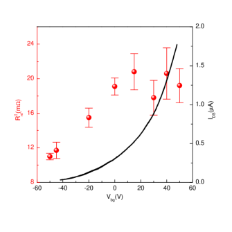
In order to obtain the transfer characteristics, i.e. back-gate dependent conductivity of the WS2 substrate, we apply a dc voltage = 0.2 V and measured the current between the top gate contact, that touches the bottom WS2 at point D and a contact S on the BLG flake (Fig. S1(b)), and vary the back-gate voltage in order to change the resistivity of WS2. The behavior of the bottom-WS2 flake of stack A is plotted in Fig. S3.

III Spin transport measurements
For spin-valve (SV) measurements, a charge current is applied between contacts C2-C1 and a nonlocal voltage is measured between C3-C4 (Fig. S1(a)). First an in-plane magnetic field 0.2 T is applied along the easy axes of the ferromagnetic (FM) electrodes (+y-axis), in order to align their magnetization along the field. Now, is swept in the opposite direction (-y-axis) and the FM contacts reverse their magnetization direction along the applied field, one at a time. This magnetization reversal appears as a sharp transition in or in the nonlocal resistance . The spin-signal is , where represents the value of the two level spin-valve signal, corresponding to the parallel (P) and anti-parallel (AP) magnetization of the FM electrodes. In the nonlocal measurement geometry the spin-signal is given by:
| (S2) |
Here is the spin-relaxation length for the in-plane spins in graphene and is the contact polarization of injector and detector electrodes for in-plane spins, is the graphene sheet-resistance and is the width of spin-transport channel.
For Hanle spin-precession measurements, for a fixed P (AP) configuration, an out-of-plane magnetic field is applied and the injected in-plane spin-accumulation precesses around the applied field. From these measurements, we obtain the spin diffusion coefficient and in-plane spin-relaxation time , and estimate the spin-relaxation length = . Using this in Eq. S2, we obtain the contact polarization 3-5 % for in-plane spin-transport. We would like to make a remark here that some of the contacts in stack A have the opposite (i.e., negative) sign of for in-plane spin-transport. The origin of the negative sign is nontrivial and possibly could be due to the specific nature of the FM tunnel barrier interface with the graphene-on-TMD.

SV measurements as a function of (stack B) are summarized in Figs. S4 and S5 for stack A and stack B, respectively. For both samples, there is no significant change in the spin-signal within the range 40V. For stack A, the FM contacts have low resistance ( 1k) and this is the reason that there is a modest increase in at higher charge carrier density due to the suppressed contact-induced spin-relaxation Maassen et al. (2012); Omar and van Wees (2017). Both measurement do not exhibit any measurable signature of spin-absorption due to the conductivity modulation of the underlying TMD substrate.
IV Generalized Stoner-Wohlfarth Model for extracting magnetization angle
In this section, we describe the basics of Stoner-Wohlfarth (SW) model, and extend it for three dimensional case in order to extract the magnetization-direction of a bar-magnet in presence of an external magnetic field.
The total energy of a ferromagnet in a magnetic field is expressed as:
| (S3) |
where and are the contributions from Zeeman and anisotropic energy, respectively.
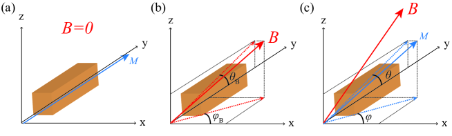
First a magnetic field is applied which makes an angle with the x-axis and an angle (Fig. S6(b)), having its components along and axes, respectively. Here can be parameterized with respect to ) in the following way:
| (S4) |
For a ferromagnetic bar with its anisotropic constants and along x,y and z axis, respectively, and making an angle and with the x, y and z axis, respectively, be generalized to a three-dimensional form as:
| (S5) |
Now we write down the expression for and which have contributions from and .
At () makes the azimuthal angle with the x-axis in the x-y plane and polar angle with the y-axis in the y-z plane (Fig. S6(c)). Therefore, = = . The anisotropic and Zeeman energy terms can again be parameterized with respect to in to a three-dimensional form:
| (S6) | ||||
and
| (S7) | ||||
Now the expressions in Eq.s LABEL:anisotropy and S7 can be substituted to Eq. S5 and a full functional form of can be obtained.
In order to obtain which correspond to min(), we solve for the global energy minima of Eq. S5 by imposing two following conditions:
| (S8) | ||||
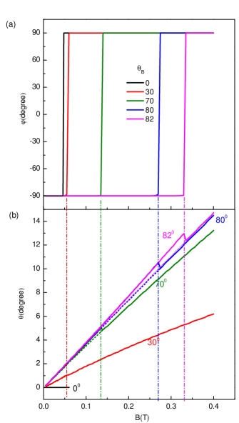
Since has its easy axis along y-axis, . We use = 510 as reported in literature Kittel (2004). In order to obtain , we use the saturation magnetic field of the FM electrodes along z-direction, i.e. 1.5 T for the thickness (65nm) of the FM electrodes, and use the relation Raes et al. (2016). In order to obtain , we use the in-plane switching fields of FM electrodes, and use them as the only free parameter in the model to obtain the in-plane magnetization switching as obtained in measurements.
V Oblique Spin-valve measurements
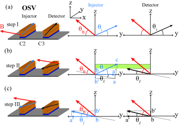
Before starting the Oblique Spin-valve (OSV) measurements, we set the initial of the FM electrodes along +y-axis, i.e. along their easy magnetization-axis. Here, the measured spin-signal .
Step-I: We apply a magnetic field in the opposite direction which makes an angle with the -y-axis, as shown in Fig. S8(a). Here, we assume that both injector and the detector due to their identical thickness have the same out-of-plane anisotropy value . As the magnitude of increases, the magnetization of both injector and detector FM electrodes makes a finite angle with respect to its initial direction (+y-axis), and the injected spins have their quantization axis along (Fig. S8(a)). Now, the measured spin-signal in the parallel configuration can be expressed as:
| (S9) |
Here, is the functional form for the in-plane (out-of-plane) spin precession of dynamics.
Step-II: Due to different widths of the FM electrodes, they have different in-plane anisotropies and different switching fields. At a certain magnetic field, the magnetization of the detector reverses the direction of its y-component. Now, the detector magnetization subtends an angle with the negative y-axis (Fig. S8(b)). This activity is seen as a switch due to the direction reversal of both in-plane and out-of-plane magnetization component with respect to its initial orientation. The factorization of in-plane and out-of-plane components can be understood via the presented vector diagram in Fig. S8(b) in following steps:
-
•
The injector electrode injects the spin signal along , represented by the blue arrow b-c in Fig. S8(b).
-
•
The detector measures the projection of the injected spin-signal which has its quantization axis at , along the detector magnetization axis along b-a, shown as a black dashed line in Fig. S8(b). Now the magnetization axis, along which the spin-signal is measured becomes:
(S10) where are the unit vectors along y and z-axis, respectively. Since the in-plane and out-of-plane spin-signals have magnitudes and , the spin-signal measured by the detector becomes:
(S11)
Step-III: Finally, the injector electrode reverses its magnetization and both electrodes have their magnetizations pointing in the same direction, and making an angle with the device plane Fig. S8(c). The spin-signal has the same expression as in Eq. S9, except is replaced with . The desired spin valve signal can be obtained by subtracting Eq. S11 with Eq. S9 with appropriate values, obtained from Fig. S7 at corresponding magnetization switching fields.
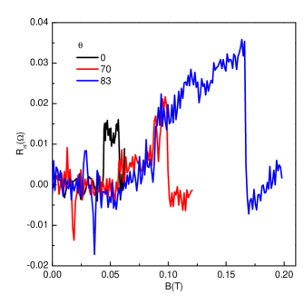
A data set for the oblique spin valve measurements is shown in Fig. S9. As expected by the simulation results in Fig. S7, the magnetization switching follows the relation , where is the magnetization switching field 40 mT for the in-plane spin valve (black curve in Fig. S9). The measured signal has contribution from both in-plane and out-of-plane magnetization switching. As suggested by the simulation results, the magnetic field dependent background in the measurement has similar trend as observed in Fig. S7(b)) due to the field-dependent magnetization angle, and has contribution of the out-of-plane spin-signal. The processed data after removing this field dependence is shown in Fig.3(a) of the main text which shows a clear enhancement in the measured spin valve signal magnitude. This is a consequence of large spin-life time anisotropy present in the system, and is discussed in the manuscript in detail.
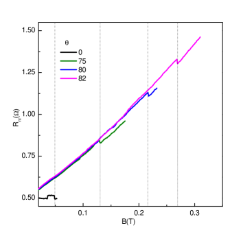
An additional set of OSV measurements for a different region (on the right side) of stack A is shown in Fig. S10. For this set the FM electrodes at 83∘ switch earlier than the expected switching field, i.e. 300 mT, and using the angles obtained in Fig. S7 and in the region, the analysis yields 244 and 4 ns. The overestimation of is probably due to earlier switching of the FM electrode. However, the effect of anisotropy can be clearly seen in the measurement.
VI Nonlocal Hanle signal versus orbital magnetoresistance
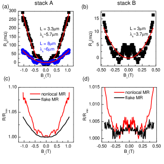
A negligible charge background signal due to the orbital magnetoresistance of the graphene flake is present at the applied (Fig. S11).
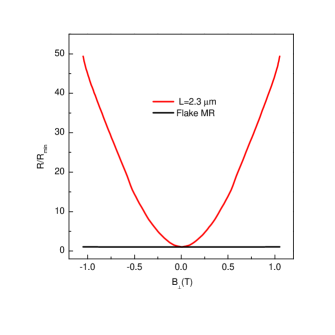
Here, for the same channel increases almost 50 fold whereas there is hardly any change in the background MR signal(Fig. S11). Therefore the observed increase in at high is clearly not due to the orbital magnetoresistance of the graphene-flake.
VII Estimating out-of-plane spin relaxation time via Hanle measurements
It is already explained in the previous section that at a nonzero magnetic field applied at an angle with the device plane, the magnetization vector makes a finite angle with the device plane (Fig. S6). Here, we represent a specific case with for Hanle measurements. Here, we would represent as and assume that both injector and detector behave identically and their vectors make same angle . At 0, has its quatization axis not in the device plane, it also electrically injects a nonzero out-of-plane spin-signal. If for both injector and detector were pointing perpendicular to the device plane, the measured nonlocal signal would be written as:
| (S12) |
Here is the spin-relaxation length for the out-of-plane spins in graphene and is the contact polarization of injector and detector electrodes, which is obtained via in-plane spin-transport measurements. is the magnetoresistance (MR) of the graphene flake in presence of the out-of-plane magnetic field. However, in general for the values of 1.2 T due to limitations of the electromagnet in the setup, we inject and detect only a fraction of that is proportional to , and the in-plane spin-signal that is proportional to and gets dephased by .
FM contacts also measure charge-related MR and a constant spin-independent background due to current spreading and homogeneous current distribution even in the nonlocal part of the circuit. This contribution can be represented as:
| (S13) |
Therefore, the total measured nonlocal signal is:
| (S14) |
Here +(-) before the expression for the in-plane spin signal is for P(AP) magnetization configuration of the injector-detector electrodes and is the expression for Hanle precession dynamics. The second term can be omitted from Eq. S14 by measuring for both P and AP configurations of FM electrodes and then averaging them out. Via this exercise, we get rid of the in-plane spin signal and get the following expression:
| (S15) |
At = 0 T, and , Eq. S15 reduces to:
| (S17) |
Using Eq. S12, we obtain the final expression:
| (S18) |
VIII Estimation of Valley-Zeeman and Rashba SOC strengths
In graphene/TMD heterostructures, different spin-orbit coupling strengths are induced in graphene in the in-plane and out-of-plane directions because of weak van der Waals interactions with the contacting TMD Cummings et al. (2017). This effect can be measured in the anisotropy of in-plane () and out-of-plane spin-relaxation time () using the following relation:
| (S19) |
Here and are spin-orbit coupling strengths corresponding to the out-of-plane and in-plane spin-orbit field, respectively. is the intervalley scattering time, and is the momentum relaxation time of electron.
From the charge and spin transport measurements, we obtain the diffusion coefficient 0.01-0.03 m2V-1s-1. Following the relation , where =106 m/s is the Fermi velocity of electrons in graphene, we obtain 0.01-0.03 ps. Typically, for strong intervalley scattering, we can assume the relation Cummings et al. (2017), and estimate 0.05-0.15 ps. From the spin-transport experiments, we already know 1 ns and 30 ps. We can now estimate and independently by assuming that the spin-relaxation is dominated by the Dyakonov Perel mechanism Cummings et al. (2017), i.e. using the relations and , respectively. We obtain 100 and 350. The obtain values are of similar order magnitude as reported in literature Omar and van Wees (2018); Zihlmann et al. (2018); Cummings et al. (2017).
References
- Gurram et al. (2016) M. Gurram, S. Omar, S. Zihlmann, P. Makk, C. Schönenberger, and B. J. van Wees, Phys. Rev. B 93, 115441 (2016).
- Zomer et al. (2014) P. J. Zomer, M. H. D. Guimarães, J. C. Brant, N. Tombros, and B. J. van Wees, Appl. Phys. Lett. 105, 013101 (2014).
- Maassen et al. (2012) T. Maassen, I. J. Vera-Marun, M. H. D. Guimarães, and B. J. van Wees, Phys. Rev. B 86, 235408 (2012).
- Omar and van Wees (2017) S. Omar and B. J. van Wees, Phys. Rev. B 95, 081404 (2017).
- Kittel (2004) C. Kittel, Introduction to Solid State Physics (Wiley, 2004).
- Raes et al. (2016) B. Raes, J. E. Scheerder, M. V. Costache, F. Bonell, J. F. Sierra, J. Cuppens, J. Van de Vondel, and S. O. Valenzuela, Nat. Commun. 7, 11444 (2016).
- Cummings et al. (2017) A. W. Cummings, J. H. Garcia, J. Fabian, and S. Roche, Phys. Rev. Lett. 119, 206601 (2017).
- Omar and van Wees (2018) S. Omar and B. J. van Wees, Phys. Rev. B 97, 045414 (2018).
- Zihlmann et al. (2018) S. Zihlmann, A. W. Cummings, J. H. Garcia, M. Kedves, K. Watanabe, T. Taniguchi, C. Schönenberger, and P. Makk, Phys. Rev. B 97, 075434 (2018).