Terahertz Surface Modes and Electron-Phonon Coupling in Bi2Se3(111)
Abstract
We present a combined experimental and theoretical study of the surface vibrational modes of the topological insulator (TI) Bi2Se3 with particular emphasis on the low-energy region below 10 meV that has been difficult to resolve experimentally. By applying inelastic helium atom scattering (HAS), the entire phonon dispersion was determined and compared with density functional perturbation theory (DFPT) calculations. The intensity of the phonon modes is dominated by a strong Rayleigh mode, in contrast to previous experimental works. Moreover, also at variance with recent reports, no Kohn-anomaly is observed. These observations are in excellent agreement with DFPT calculations. Besides these results, the experimental data reveal—via bound-state resonance enhancement—two additional dispersion curves in the gap below the Rayleigh mode. They are possibly associated with an excitation of a surface electron density superstructure that we observe in HAS diffraction patterns. The electron-phonon coupling paramenter = 0.23 derived from our temperature dependent Debye-Waller measurements compares well with values determined by angular resolved photoemission or Landau level spectroscopy. Our work opens up a new perspective for THz measurements on 2D materials as well as the investigation of subtle details (band bending, the presence of quantum well states) with respect to the electron-phonon coupling.
I Introduction
Bi2Se3 (Figure 1) is categorised as a three-dimensional topological insulator, a new state of quantum matter with a bulk gap and spin-orbit split surface states forming a Dirac cone across the gapHasan and Kane (2010); Moore (2009). The interaction of electrons with surface phonons in Bi2Se3 has been studied intensively due to its important role in transport properties and possible constraints for potential applications in a variety of nanotechnologiesHatch et al. (2011); Pan et al. (2012); Chen et al. (2013); Kondo et al. (2013); Zhu et al. (2012); Giraud et al. (2012); Di Pietro et al. (2013). Bismuth selenide as well as telluride alloys are classical thermoelectric materialsKadel et al. (2010); Mishra et al. (1997) with a large Seebeck coefficient and, as such, they have been used in thermoelectric refrigeration for a long timeGoldsmid (1964). However, to fully understand the thermoelectric properties of Bi2Se3 thin films and nanoscale devicesLiang et al. (2016); Tang et al. (2015), information on the surface phonon dispersion curves and the electron-phonon (e-ph) interaction is crucialLiang et al. (2016); Minnich et al. (2009); Hsiung et al. (2015).
So far experimental information about the surface phonon dispersion curves of Bi2Se3(111) was limited to previous helium atom scattering (HAS) studies by Zhu et al.Zhu et al. (2011, 2012), in the low energy part of the phonon spectrum. These studies suggested the presence of a deep Kohn anomaly in the 7.5 meV optical phonon branch (S2) coupled to the electronic (spin-forbidden) transition across the Dirac coneZhu et al. (2011). However, existing first-principle calculations of Bi2Se3(111) phonon dispersion curves, do not show any evidence of Kohn anomalies in the S2 branchHeid et al. (2017).
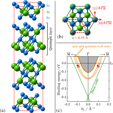
A convenient parameter to characterise the e-ph coupling strength is the mass-enhancement Grimvall (1981) and in recent years it was demonstrated that HAS from conducting surfaces can directly measure the mode-selected e-ph coupling constants Sklyadneva et al. (2011); Tamtögl et al. (2013), besides the surface phonon dispersion curvesBenedek and Toennies (2018). Moreover the temperature-dependence of the HAS Debye-Waller factor was shown to provide the global e-ph coupling constant at the surface of thin metal filmsBenedek et al. (2018); Benedek and Toennies (2018) and topological insulatorsTamtögl et al. (2017). Yet the large as estimated based on the Kohn anomalyZhu et al. (2012) is at odds with theoretical findings that indicate that the major contribution to comes from the higher optical phonon branchesHeid et al. (2017), especially when the Fermi level crosses the surface quantum-well states above the conduction band minimum (see Figure 1(c)). The situation is actually met in recent high-resolution 3He-spin scattering studies on Bi2Te3(111), where the weak signature of a Kohn anomaly is detected in the surface longitudinal acoustic resonanceTamtögl et al. (2018), also not found in adiabatic ab-initio calculations of the phonon branches.
In order to elucidate these conflicting results, we have undertaken a HAS study of the surface phonon dispersion curves and the e-ph interaction of Bi2Se3(111). Supersonic neutral He atom beams with incident energies in the range have been used to probe low-energy surface excitations with the best available resolution, while being an inert completely nondestructive probeFarías and Rieder (1998); Benedek and Toennies (2018). The technique allows to measure most of the surface phonon branches in the acoustic and optical regions. Low-energy He atoms impinging on a conducting surface are exclusively scattered by the surface charge densityMayrhofer-Reinhartshuber et al. (2013); Tamtögl et al. (2013) and inelastic scattering from surface phonons only occurs via the phonon-induced charge density oscillations, i.e., via the e-ph interaction. It is in this way that inelastic HAS provides a first-hand information on the e-ph interaction, with the neutral He atoms acting as a sort of local mechanical probe on the electron density.
Energy and momentum, inelastically exchanged by He atoms with the surface can, however, be retained by the electron system in the form of low-energy collective excitations. In principle, the HAS signal from this kind of excitations is expected to be quite small. Nevertheless, an increased e-ph interaction due to surface quantum-well statesSilkin et al. (2004) in combination with an enhancement from HAS bound-state resonancesEvans et al. (1983), suggests to assign two branches of low-energy modes in the gap well below the Rayleigh waves (RW) to some sort of collective electronic excitations. Actually anomalous acoustic plasmons have been recently reported in Bi2Se3(111) by Jia et al.Jia et al. (2017), from high-resolution electron energy-loss spectroscopy, although these modes turn out to be superimposed in the first Brillouin zone onto the RW branch.
Plasmons in a two-dimensional electron gas (2DEG) with a dispersion (2D plasmons) have been predicted long ago by Frank SternStern (1967); Ando et al. (1982). Later it was shown that the coupling of 2DEG plasmons arising from two different quantum-well minibands, as found in semiconductor surface accumulation layers, yield a surface plasmon pair: a 2D plasmon and an acoustic surface plasmon (ASP) with a linear dispersion above the upper edge of the single-particle excitation spectrumShvonski et al. (2019); Yu and Hermanson (1990). Similarly the coupling of a 2DEG at a metal surface coupled to the underlying 3D electron gas yields an ASP in addition to the ordinary surface plasmonSilkin et al. (2004); Pitarke et al. (2006); Wang et al. (2011); Diaconescu et al. (2007). As discussed below, the assignment of the two additional low-energy branches as collective polaron excitation recently suggested by Shvonski et al.Shvonski et al. (2019), although plausible in semimetals with a large dielectric constant, definitely requires further ad-hoc studies, possibly with even higher resolution as available, e.g., with 3He spin-echo spectroscopyTamtögl et al. (2018).
II Results and discussion
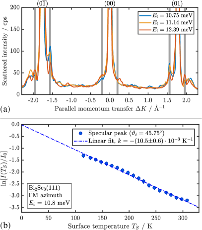
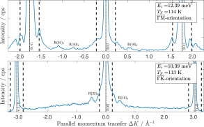
Figure 2(a) shows several diffraction scans along the azimuth plotted versus momentum transfer , while in Figure 2(b) the temperature dependence of the specular peak intensity is plotted, which can be used to extract the electron-phonon coupling constant (section Electron-phonon coupling). The diffraction scans in Figure 2(a) have been measured at three different incident energies , at a sample temperature of 113 K. The intensity scale has been scaled to show additional features with smaller intensity. Besides some features assigned to bound-state resonances and kinematic focusing, which are easily recognised due to the strong dependence of their position on the incident energyMayrhofer-Reinhartshuber et al. (2013), there are features that occur at fixed values of , independently of with a distance of about from the specular and first order diffraction peaks, as indicated by the vertical shaded regions (further diffraction scans, including also the azimuth can be found in the supplementary information).
We recently observed with HAS a multivalley charge density wave (CDW) in Sb(111) originating from the -point electron pockets giving rise to additional peaks in the diffraction patternTamtögl et al. (2019). In Bi2Se3(111), however, no carrier pockets exist besides the Dirac cone and the quantum-well minibands occurring around the zone center (see Figure 1(c)). The latter provide nesting wavevectors of about between states of equal spin, which correspond fairly well to the parallel momentum transfers of the satellites observed aside the peaks in HAS diffraction spectra (and likely also aside the specular peak, despite the coincidence with bound-state resonances) (Figure 2(a)). It should be noted, however, that the observation of satellite peaks whose position is independent of the HAS incident energy is by itself indicative of a long-period superstructure of the electron density, possibly incommensurate or weakly commensurate with the surface atomic lattice. Charge density oscillations as low as atomic units, presently accessible to HAS, can in principle sustain very low-energy collective phase and amplitude excitations in the meV spectral rangeTamtögl et al. (2019), and possibly suggest an assignment of the present low-energy branches.
II.1 Time-of-flight measurements and phonon dispersion curves
The phonon energies were determined by performing time-of-flight (TOF) measurements over a wide range of incident angles between the first-order diffraction peaks and at various beam energies. The phonon dispersion was then obtained by calculating the parallel momentum transfer for each extracted phonon energy from the conservation laws of energy and parallel momentum providing the so-called scan curve for planar scattering (see (1) and Refs. Tamtögl et al. (2013); Safron (1996)).
In Figure 3(a) an example of a TOF spectrum after conversion to the energy transfer scale is shown. The measurement was taken in the high symmetry direction with an incident beam energy and at an incident angle of . The TOF spectrum consists of several peaks which are located on the creation () as well as the annihilation () side. The peak at zero energy transfer corresponds to elastically scattered helium atomsFarías and Rieder (1998); Tamtögl et al. (2018). The scan curve, shown in the two centre panels of Figure 3 for phonon annihilation (blue) and creation (red) events, associates each phonon event with a specific momentum transfer . The scan curve has been backfolded into the irreducible part of the Brillouin zone and is plotted on top of the calculated dispersion. The different symbols on the scan curves, marking the main inelastic features, have been associated to phonons of different character and polarisation.
The large peaks in the TOF spectra marked with the red circles in Figure 3, correspond to the Rayleigh wave (RW) as seen in the DFPT calculations. Note that in the present TOF spectra the RW exhibits typically the largest intensity of all inelastic events (cfr. the intensities in Figure 3(a)). There is a fair correspondence between the present HAS data and those previously reported by Zhu et al.Zhu et al. (2011). Curiously Zhu et al. stated that the RW is not observed, whereas it appears in their plot, though with only a few data points, in reasonable agreement with the present one in the direction; it also occurs in the direction, once it is recognised that there is an avoided crossing, so that the RW at is not the lowest mode. There is however an important difference with respect to Zhu et al.Zhu et al. (2011): Present HAS data do not show any evidence of a Kohn anomaly in the meV branch for wavevectors around and associated with the nesting at the Fermi level across the Dirac cone (or more likely across the parabolic dispersion of surface quantum-well statesKing et al. (2011); Bianchi et al. (2010)).
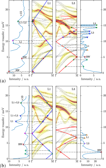
Figure 4 shows the entire experimental surface phonon dispersion (symbols) superimposed onto the DFPT calculations (grey lines). The different symbols have been associated to phonons of different character and polarisation based on the proximity to particular modes of the DFPT calculations. In total, we are able to distinguish at least 8 different branches.
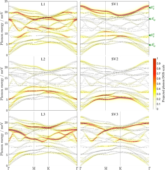
The polarisation analysis of the calculated surface phonon modes can be found in Figure 5 where the intensity of each polarisation projected onto the corresponding layer is given by the colour code. The left column shows the longitudinal polarisations for the first (L1), second (L2), and third (L3) layer. The right column shows the shear vertical polarisation for the first three layers (SV1-SV3), while the shear horizontal polarisation can be found in the supporting information. The theoretical dispersion curves are seen to agree quite well with the HAS data and also with the experimental Raman-active modes at (green triangles in Figure 5 according toBoulares et al. (2018)).
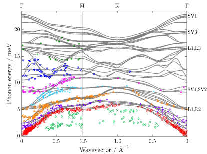
A closer comparison of the experimental data points in Figure 4 with Figure 5 shows that mainly phonon events with the largest amplitude in the two topmost layers of the sample are observed in the experiment. In particular in the low energy region ( meV), most contributions come from phonons with the largest amplitude in the second layer (L2, SV2), which is a Bi layer and therefore about times heavier than the first Se layer. The most prominent mode in the TOF spectra, the RW, corresponds predominantly to L and SV polarisations, due to its elliptical polarisation, with a particularly strong SV2 component at the Brillouin zone boundary.
Note that the calculation does not reproduce the Kohn anomaly reported by Zhu et al.Zhu et al. (2011) (see the SI for calculations with SOC), in agreement with other recent ab-initio calculations including SOC by Heid et al.Heid et al. (2017) as well as with the experimental and theoretical studies of Bi2Te3(111)Tamtögl et al. (2018). Heid et al.Heid et al. (2017) suggested that the Kohn anomaly observed by Zhu et al.Zhu et al. (2011, 2012) may be connected to a strong e-ph interaction in the doped bulk material rather than to a surface state. They actually showed that the largest contribution to the e-ph coupling comes from an in-plane polar-type branch in the optical region between 10 and 18 meVHeid et al. (2017).
Indeed the anomalously strong dispersion of the optical branches in that region (Figure 5), also found in Bi and Sb telluridesTamtögl et al. (2018); Campi et al. (2018) may be regarded as a manifestation of e-ph interaction.
In the acoustic region and the long wavelength limit (close to ) the dispersion relation of the RW is linear. Its slope provides the RW group velocity in the two symmetry directions and :
In order to appreciate the degree of localisation of the RW in the two symmetry directions, these values are to be compared with the corresponding speeds of sound. The present DFPT values (compared with values in parentheses derived from the available elastic constantsGao et al. (2016)) are:
It appears that the RW has a velocity in the direction smaller than both transverse bulk values and is therefore a localised surface wave, whereas in the direction it has a velocity larger than that of the SH transverse sound, and is therefore a pseudo-surface wave (PSW)Farnell (1970, 1978). Actually in the absence of mirror symmetry for the sagittal plane in this direction, the RW is a resonance. The fact may have suggested (see Zhu et al.Zhu et al. (2011, 2012)) that in Bi2Se3(111) the RW is suppressed but the present comparison with the DFPT calculation confirms that the RW is actually observed in both directions, though as a resonance along . Values for the bulk longitudinal () and transverse () group velocities of Bi2Se3 have also been reported in the framework of the isotropic elastic continuum theoryGiraud et al. (2012); Glinka et al. (2015). In this approximation the corresponding RW velocity, obtained by solving the cubic Rayleigh equation,Maradudin and Stegeman (1991) would be in any direction.
II.2 Low-energy branches
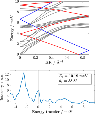
The measured HAS-TOF spectra displayed in Figure 3 show also distinct peaks yielding two branches of elementary excitations with an energy below the RW branch (green diamonds in Figure 4). On the basis of present DFPT surface phonon dispersion curves, they cannot be attributed to any possible phonon branch of the ideal surface. HAS from conducting surfaces exclusively occurs through the interaction (mostly Pauli repulsion) with the surface electron density, and therefore also electronic excitations in the THz range can be observed by HAS, with a resolution and sensitivity to charge density oscillations in the atomic units range.
Actually the observed low-energy branches are reminiscent of those recently observed with HAS in Sb(111), which have been attributed to elementary excitations (phasons/amplitons) of a multi-valley CDWTamtögl et al. (2019). The concomitant presence of a commensurate component associated with the -point electron pockets at the Fermi level, and an incommensurate one due to the hole pockets along the direction, allows for collective excitations with a comparatively small gap at . On the other hand no low-energy phason/ampliton modes have been detected with HAS for the perfectly commensurate multivalley CDW reported in the quasi-1D surface Bi(114)Hofmann et al. (2019), discommensuration being a requisite for depinning and a vanishing/small gap at . Bi2Se3(111) has no pocket states at the Fermi level, besides the rings around of the surface topological Dirac and the quantum-well statesKing et al. (2011); Bianchi et al. (2010). The satellites near the HAS diffraction peaks (see Figure 2(a)) suggest some long-period charge-density structures and possibly low-energy collective excitations. In order to detect the associated, seemingly small inelastic features in the TOF spectra, we rely on the bound-state resonance enhancement method (Ref. Evans et al. (1983) and Chap. 10 of Ref. Benedek and Toennies (2018)), applicable to highly corrugated surfaces and successfully used to detect with HAS high-energy optical surface modes in ionic crystalsBracco et al. (1986); Benedek and Toennies (2018). The complete set of He-surface bound states has been measured previouslyRuckhofer et al. (2019).
Bound-state inelastic resonances occur in the HAS-TOF spectrum, with a possibly large enhancement of the inelastic intensities, at the locus of intersections of the scan curve (1) Tamtögl et al. (2013) with the inelastic bound-state resonance condition (2) (see Chap. 30 of Ref. Benedek and Toennies (2018)). For elementary excitations with an energy and wavevector the equations become:
| (1) |
| (2) |
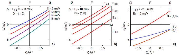
At the mentioned intersection of (1) and (2), an elementary excitation with assists the selective adsorption of the atom of mass , incident energy , wavevector and angle into a bound state of energy , via the exchange of a surface reciprocal lattice vector . On returning the G-vector to the surface lattice, the atom is selectively desorbed from the bound state into the final angle . In Equation 2 the vector G has been conveniently expressed via its components parallel and orthogonal to the scattering plane, respectively. In Bi2Se3(111) the measured He-surface bound-state energiesRuckhofer et al. (2019) are meV for = 0, 1, 2, 3, 4, respectively. For a fixed scattering geometry (here ), Eqs. (1,2) provide, via the elimination of , the locus of intersections for any incident energy , bound state and reciprocal surface vector G.
The three panels of Figure 6 show some plots of in the direction for: (a) a given bound state (), a G vector (1,0) and different values of the incident energy ; (b) a given incident energy = 10 meV and different bound state energies; (c) a given incident energy = 10 meV and bound state and some different G-vectors, whose functions cross the phonon gap below the RW in the first BZ. In practice the phonon gap can be fully scanned by the resonance curves by varying the incident energy, so as to detect, via resonance enhancement, weak elementary excitations.
Since the low-energy data points appear to allign along two dispersion curves, independently of the incident energy, as well as of and G, rather than being spread over the entire gap, they cannot be attributed to a resonance-enhanced many-phonon background. Furthermore, frustrated translational modes of adsorbates like CO would show no dispersion and would appear at higher vibrational energiesGraham (2003). More likely these points indicate two branches of low-energy excitations associated with the surface charge-density superstructure observed in the diffraction spectra, as anticipated above.
In this respect it is worth mentioning a recent work by Shvonski et al.Shvonski et al. (2019) where it is argued that a strong e-ph interaction affecting the surface 2DEG of a 3D topological crystal allows for collective polaron excitations (plasmon-polarons). Their dispersion is predicted to be that of an acoustic plasmon running below the single-particle excitation spectrum as an effect of the polaron-polaron attractive interaction. The theoretical analysis by Shvonsky et al.Shvonski et al. (2019) is actually interpreting the recent observation with high-resolution electron energy loss spectroscopy (HREELS) by Jia et al.Jia et al. (2017) of an anomalous acoustic plasmon (AAP) mode from the topologically protected states of Bi2Se3(111), with energy between and meV (and its continuation in the second zone up to meV). The present HAS data do not permit to identify this AAP due to its superposition with the RW in the first BZ and in part with other phonon branches in its continuation.
II.3 Electron-phonon coupling
As shown in recent papersTamtögl et al. (2017); Benedek et al. (2018), the temperature dependence of the Debye-Waller (DW) exponent plotted in Figure 2(b) permits to extract for a conducting surface the mass-enhancement parameter expressing the electron-phonon coupling strength. It is related to the DW exponent by the equations:
| (3) |
where is the work functionSuh et al. (2014), the unit cell area, the He-beam specular intensity, the surface temperature, the normal component of the incident wavevector, and the number of conducting layers which contribute to the phonon-induced modulation of the surface charge density111The (bulk) carrier concentration as extracted from Hall measurements of the current sample is in the region , i.e. a particularly small conductivity in the bulk suggesting that the carrier concentration at the surface may even be larger, compared to the first generation samplesBianchi et al. (2010) which had a much larger bulk charge carrier concentration.. The latter is estimated to be , where is the Thomas-Fermi screening length characterising the surface band-bending region (here nm)Bianchi et al. (2010), the quintuple layers (QL) thickness, and the factor 2 indicates the 2DEG multiplicity as observed with ARPES in the current Bi2Se3 sampleBianchi et al. (2010).
With these values and the experimental DW derivative with respect to from Figure 2(b), we obtain . It should be noted that, unlike in the case of low-index metal surfaces, characterised by a soft-wall repulsive potential and negligible corrugation, here the large electronic corrugationRuckhofer et al. (2019) implies a hard-wall potential. In this case one needs to correct so as to account for the acceleration impressed by the attractive part of the potential on the He atom when approaching the surface turning point (Beeby correctionFarías and Rieder (1998)). Therefor is replaced by , where is the He mass and the He-surface potential well depthRuckhofer et al. (2019). With the Beeby correction it is found .
The value compares quite well with values in the literature derived from other experiments, e.g., Hatch et al. (2011), and Chen et al. (2013) from ARPES measurements and Zeljkovic et al. (2015) from Landau level spectroscopy. A theoretical study by Giraud et al.Giraud et al. (2012) with phonons calculated in the isotropic continuum limit gives , whereas for other ARPES measurements, where only Dirac states appear to be involved, values of as low as to have been foundPan et al. (2012).
From the comparison it appears that the presence of a 2DEG due to quantum-well minibands (at least two in the present analysis) plays an important role in raising the e-ph coupling strength, which is quite small when exclusively due to the Dirac topological states, to values in the range of . The same conclusion follows from the theoretical analysis by Heid et al. Heid et al. (2017), who showed that raising the Fermi level from the Dirac point to above the conduction band minimum gives a corresponding increase of from values well below to values in the range above , with a substantial contribution from interband coupling and in very good agreement with the present analysis. The role of n-type doping contributing to the formation of the surface quantum-well 2DEG is quite clear in the analysis of the e-ph coupling strength in Cu-doped Bi2Se3 , where an analysis based on the McMillan formula McMillan (1968), indicates a value for as large as Pan et al. (2012).
III Conclusions
In summary, we have determined the surface phonon dispersion curves of Bi2Se3 along both high symmetry directions, where the largest inelastic scattering intensity is provided by the Rayleigh wave. Thus our measurements show in contrast to previous studies that the Rayleigh mode exists and is a localised surface mode in one of the high-symmetry directions (), while in the other high-symmetry direction it is actually a pseudo-surface wave (). Comparison with density functional perturbation theory calculations shows excellent agreement with the experimental data. In addition to the phonon-related losses, we observe two additional dispersion curves in the gap well below the Rayleigh mode. These two low-energy branches may correspond to collective low-energy excitations of surface electrons.
The appearance of these collective electronic excitations in an unprecedentedly low energy region is probably associated with a small surface charge density and an appreciable electron-phonon coupling (). However, much more detailed experiments and theoretical analysis will be needed in order to fully understand these excitations; e.g., what is the influence of the carrier concentration upon doping and what is the role of both the Dirac and the quantum-well states, with the latter providing a much larger electron-phonon interaction than the former. The analysis advocates for a more systematic study by means of elastic and inelastic HAS spectroscopy of the surface structure, the low-energy collective excitations, and the electron-phonon interaction of interesting 2D materials, where the superior space and energy resolution of HAS is hardly attainable with other current surface probes.
IV Methods
IV.1 Experimental Details
The reported measurements were performed on a HAS apparatus which generates a nearly monochromatic beam of 4He that is scattered off the sample surface in a fixed source-sample-detector geometry. The beam is produced in a supersonic expansion of He through a nozzle followed by sampling the core of the supersonic expansion via a skimmer. For a detailed description of the apparatus please refer toTamtögl et al. (2010).
Energy dispersive measurements for inelastic scattering can be performed using TOF measurements with a pseudo-random chopper disc. After deconvolution with the pseudo random chopper sequence, the TOF signal is further transformed to an energy transfer scale which allows to determine inelastic (phonon) scattering eventsTamtögl et al. (2010). The scattering spectra were mainly taken with the crystal at room temperature, while a few spectra were taken with the sample cooled down to . The incident He beam energy was varied between 10 and 18 meV.
The crystal structure of Bi2Se3 is rhombohedral, formed of QL which are bound to each other through weak van der Waals forcesMichiardi et al. (2014). The hexagonal unit cell of the Bi2Se3 crystal, shown in Figure 1, consists of 3 QLs. Each QL is terminated by Se atoms, giving rise to the (111) cleavage plane that exhibits a hexagonal structure ( at room temperatureChen et al. (2011), see Figure 1(b)). The Bi2Se3 crystal was attached onto a sample holder using thermally conductive epoxy. The sample holder was then inserted into the transfer chamber using a load-lock system and cleaved in-situTamtögl et al. (2016). The sample can be heated using a button heater on the backside of the crystal or cooled down to via a thermal connection to a liquid nitrogen reservoir. The sample temperature was measured using a chromel-alumel thermocouple.
IV.2 Computational Details
The surface dynamical properties of Bi2Se3 were studied using DFPT calculationsBaroni et al. (2001) withing the Quantum-ESPRESSO packageGiannozzi et al. (2009). Norm-conserving pseudopotentials and the Perdew-Burke-Ernzerhof (PBE) approximation Perdew et al. (1996) for the exchange and correlation functional were used as implemented in the Quantum-ESPRESSO package. The surface phonon dispersion was calculated using a slab consisting of 3 QLs separated from its periodic replica by 20 Å of vacuum, without the inclusion of spin-orbit corrections (SOC) (see also the SI for calculations with SOC). For an accurate calculation of the surface lattice vibrations, in principle both SOC and van der Waals (vdW) corrections are necessary, both due to the presence of heavy elements in the compound and the latter to fully account for the weak bonds between the individual quintuple layers. However, as thoroughly discussed for Bi2Te3(111)Tamtögl et al. (2018), it appears that for layered crystals with heavy elements SOC alone gives a general softening of the phonon spectrum, compensated by the inclusion of vdW correction, so that satisfactory results are obtained at a minor computational cost without both SOC and vdW corrections and with a better agreement with experimentAlcántara Ortigoza et al. (2014); Tamtögl et al. (2013). Also for Bi2Se3 better agreement with the experiment is achieved with no SOC and no vdW corrections (see subsection II.1), likely due to a compensation of errors between the underbinding often characterising PBE functionals and SOC contributions and the overbinding due to vdW forcesTamtögl et al. (2018). More precisely, the effect of SOC was found however to be weak for the low energy surface vibrational modes of typical TIs such as Bi2Te3 and Sb2Te3Campi et al. (2018); Tamtögl et al. (2018) while on the other hand it was shown that vdW corrections become important for an exact description of the low energy optical modes of Bi2Te3Tamtögl et al. (2018).
Associated Content
Supporting Information accompanies this paper including additional DFPT calculations, as well as additional spectra and further details about the helium atom scattering experiments.
Acknowledgment
We are grateful to Prof. Evgueni V. Chulkov (DIPC) and Prof. Krzysztof Kempa (Boston College) for useful discussions. The authors are grateful for financial support by the FWF (Austrian Science Fund) within the project P29641-N36 and A.T acknowledges financial support within the project J3479-N20. We would like to thank the Aarhus University Research Foundation, VILLUM FOUNDATION via the Centre of Excellence for Dirac Materials (Grant No. 11744) and the SPP1666 of the DFG (Grant No. HO 5150/1-2) for financial support. M. Bremholm acknowledges financial support from the Center of Materials Crystallography (CMC) and the Danish National Research Foundation (DNRF93).
References
- Hasan and Kane (2010) M. Z. Hasan and C. L. Kane, Rev. Mod. Phys. 82, 3045 (2010).
- Moore (2009) J. Moore, Nat. Phys. 5, 378 (2009).
- Hatch et al. (2011) R. C. Hatch, M. Bianchi, D. Guan, S. Bao, J. Mi, B. B. Iversen, L. Nilsson, L. Hornekær, and P. Hofmann, Phys. Rev. B 83, 241303 (2011).
- Pan et al. (2012) Z.-H. Pan, A. V. Fedorov, D. Gardner, Y. S. Lee, S. Chu, and T. Valla, Phys. Rev. Lett. 108, 187001 (2012).
- Chen et al. (2013) C. Chen, Z. Xie, Y. Feng, H. Yi, A. Liang, S. He, D. Mou, J. He, Y. Peng, X. Liu, et al., Sci. Rep. 3, 2411 (2013).
- Kondo et al. (2013) T. Kondo, Y. Nakashima, Y. Ota, Y. Ishida, W. Malaeb, K. Okazaki, S. Shin, M. Kriener, S. Sasaki, K. Segawa, and Y. Ando, Phys. Rev. Lett. 110, 217601 (2013).
- Zhu et al. (2012) X. Zhu, L. Santos, C. Howard, R. Sankar, F. C. Chou, C. Chamon, and M. El-Batanouny, Phys. Rev. Lett. 108, 185501 (2012).
- Giraud et al. (2012) S. Giraud, A. Kundu, and R. Egger, Phys. Rev. B 85, 035441 (2012).
- Di Pietro et al. (2013) P. Di Pietro, M. Ortolani, O. Limaj, A. Di Gaspare, V. Giliberti, F. Giorgianni, M. Brahlek, N. Bansal, N. Koirala, S. Oh, P. Calvani, and S. Lupi, Nature Nanotechnology 8, 556 (2013).
- Kadel et al. (2010) K. Kadel, L. Kumari, W. Li, J. Y. Huang, and P. P. Provencio, Nanoscale Res Lett 6, 57 (2010).
- Mishra et al. (1997) S. K. Mishra, S. Satpathy, and O. Jepsen, J. Phys.: Condens. Matter 9, 461 (1997).
- Goldsmid (1964) H. J. Goldsmid, Thermoelectric Refrigeration (Springer, 1964).
- Liang et al. (2016) J. Liang, L. Cheng, J. Zhang, H. Liu, and Z. Zhang, Nanoscale 8, 8855 (2016).
- Tang et al. (2015) H. Tang, X. Wang, Y. Xiong, Y. Zhao, Y. Zhang, Y. Zhang, J. Yang, and D. Xu, Nanoscale 7, 6683 (2015).
- Minnich et al. (2009) A. J. Minnich, M. S. Dresselhaus, Z. F. Ren, and G. Chen, Energy Environ. Sci 2, 466 (2009).
- Hsiung et al. (2015) T.-C. Hsiung, C.-Y. Mou, T.-K. Lee, and Y.-Y. Chen, Nanoscale 7, 518 (2015).
- Zhu et al. (2011) X. Zhu, L. Santos, R. Sankar, S. Chikara, C. . Howard, F. C. Chou, C. Chamon, and M. El-Batanouny, Phys. Rev. Lett. 107, 186102 (2011).
- Heid et al. (2017) R. Heid, I. Y. Sklyadneva, and E. V. Chulkov, Scientific Reports 7, 1095 (2017).
- Bianchi et al. (2010) M. Bianchi, D. Guan, S. Bao, J. Mi, B. B. Iversen, P. D. King, and P. Hofmann, Nat. Commun. 1, 128 (2010).
- King et al. (2011) P. D. C. King, R. C. Hatch, M. Bianchi, R. Ovsyannikov, C. Lupulescu, G. Landolt, B. Slomski, J. H. Dil, D. Guan, J. L. Mi, E. D. L. Rienks, J. Fink, A. Lindblad, S. Svensson, S. Bao, G. Balakrishnan, B. B. Iversen, J. Osterwalder, W. Eberhardt, F. Baumberger, and P. Hofmann, Phys. Rev. Lett. 107, 096802 (2011).
- Grimvall (1981) G. Grimvall, The Electron-Phonon Interaction in Metals (North-Holland Pub. Co., 1981).
- Sklyadneva et al. (2011) I. Y. Sklyadneva, G. Benedek, E. V. Chulkov, P. M. Echenique, R. Heid, K.-P. Bohnen, and J. P. Toennies, Phys. Rev. Lett. 107, 095502 (2011).
- Tamtögl et al. (2013) A. Tamtögl, P. Kraus, M. Mayrhofer-Reinhartshuber, D. Campi, M. Bernasconi, G. Benedek, and W. E. Ernst, Phys. Rev. B 87, 035410 (2013).
- Benedek and Toennies (2018) G. Benedek and J. P. Toennies, Atomic Scale Dynamics at Surfaces (Springer Berlin Heidelberg, Berlin, Heidelberg, 2018).
- Benedek et al. (2018) G. Benedek, S. Miret-Artés, S., J. P. Toennies, and J. R. Manson, J. Phys. Chem. Lett. 9, 76 (2018).
- Tamtögl et al. (2017) A. Tamtögl, P. Kraus, N. Avidor, M. Bremholm, E. M. J. Hedegaard, B. B. Iversen, M. Bianchi, P. Hofmann, J. Ellis, W. Allison, G. Benedek, and W. E. Ernst, Phys. Rev. B 95, 195401 (2017).
- Tamtögl et al. (2018) A. Tamtögl, D. Campi, M. Bremholm, E. M. J. Hedegaard, B. B. Iversen, M. Bianchi, P. Hofmann, N. Marzari, G. Benedek, J. Ellis, and W. Allison, Nanoscale 10, 14627 (2018).
- Farías and Rieder (1998) D. Farías and K.-H. Rieder, Rep. Prog. Phys. 61, 1575 (1998).
- Mayrhofer-Reinhartshuber et al. (2013) M. Mayrhofer-Reinhartshuber, P. Kraus, A. Tamtögl, S. Miret-Artés, and W. E. Ernst, Phys. Rev. B 88, 205425 (2013).
- Silkin et al. (2004) V. M. Silkin, A. García-Lekue, J. M. Pitarke, E. V. Chulkov, E. Zaremba, and P. M. Echenique, Europhysics Letters (EPL) 66, 260 (2004).
- Evans et al. (1983) D. Evans, V. Celli, G. Benedek, J. P. Toennies, and R. B. Doak, Phys. Rev. Lett. 50, 1854 (1983).
- Jia et al. (2017) X. Jia, S. Zhang, R. Sankar, F.-C. Chou, W. Wang, K. Kempa, E. W. Plummer, J. Zhang, X. Zhu, and J. Guo, Phys. Rev. Lett. 119, 136805 (2017).
- Stern (1967) F. Stern, Phys. Rev. Lett. 18, 546 (1967).
- Ando et al. (1982) T. Ando, A. B. Fowler, and F. Stern, Rev. Mod. Phys. 54, 437 (1982).
- Shvonski et al. (2019) A. Shvonski, J. Kong, and K. Kempa, Phys. Rev. B 99, 125148 (2019).
- Yu and Hermanson (1990) H. Yu and J. C. Hermanson, Phys. Rev. B 41, 5991 (1990).
- Pitarke et al. (2006) J. M. Pitarke, V. M. Silkin, E. V. Chulkov, and P. M. Echenique, Reports on Progress in Physics 70, 1 (2006).
- Wang et al. (2011) Y. Wang, E. W. Plummer, and K. Kempa, Adv. Phys. 60, 799 (2011).
- Diaconescu et al. (2007) B. Diaconescu, K. Pohl, L. Vattuone, L. Savio, P. Hofmann, V. M. Silkin, J. M. Pitarke, E. V. Chulkov, P. M. Echenique, D. Farías, and M. Rocca, Nature 448, 57 (2007).
- Ruckhofer et al. (2019) A. Ruckhofer, A. Tamtögl, M. Pusterhofer, M. Bremholm, and W. E. Ernst, J. Phys. Chem. C 123, 17829 (2019).
- Tamtögl et al. (2019) A. Tamtögl, P. Kraus, M. Mayrhofer-Reinhartshuber, G. Benedek, M. Bernasconi, D. Dragoni, D. Campi, and W. E. Ernst, npj Quantum Mater. (2019), 10.1038/s41535-019-0168-x, in press.
- Safron (1996) S. A. Safron, Adv. Chem. Phys. 95, 129 (1996).
- Boulares et al. (2018) I. Boulares, G. Shi, E. Kioupakis, P. Lošt’ák, C. Uher, and R. Merlin, Solid State Commun. 271, 1 (2018).
- Campi et al. (2018) D. Campi, M. Bernasconi, and G. Benedek, Surf. Sci. 678, 46 (2018).
- Gao et al. (2016) X. Gao, M. Zhou, Y. Cheng, and G. Ji, Philos. Mag. 96, 208 (2016).
- Farnell (1970) G. W. Farnell, in Physical Acoustics, Physical Acoustics, Vol. 6, edited by W. P. Mason and R. N. Thurston (Academic Press, 1970) pp. 109–166.
- Farnell (1978) G. W. Farnell, in Acoustic surface waves, Topics in Applied Physics, Vol. 24, edited by A. A. Oliner (Springer-Verlag, Berlin Heidelberg, 1978) pp. 13–60.
- Glinka et al. (2015) Y. D. Glinka, S. Babakiray, T. A. Johnson, M. B. Holcomb, and D. Lederman, J. Appl. Phys. 117, 165703 (2015).
- Maradudin and Stegeman (1991) A. A. Maradudin and G. I. Stegeman, in Surface Phonons, edited by F. W. W. Kress (Springer, 1991) pp. 5–35.
- Hofmann et al. (2019) P. Hofmann, M. M. Ugeda, A. Tamtögl, A. Ruckhofer, W. E. Ernst, G. Benedek, A. J. Martínez-Galera, A. Stróżecka, J. M. Gómez-Rodríguez, E. Rienks, M. F. Jensen, J. I. Pascual, and J. W. Wells, Phys. Rev. B 99, 035438 (2019).
- Bracco et al. (1986) G. Bracco, R. Tatarek, S. Terreni, and F. Tommasini, Phys. Rev. B 34, 9045 (1986).
- Graham (2003) A. P. Graham, Surface Science Reports 49, 115 (2003).
- Suh et al. (2014) J. Suh, D. Fu, X. Liu, J. K. Furdyna, K. M. Yu, W. Walukiewicz, and J. Wu, Phys. Rev. B 89, 115307 (2014).
- Note (1) The (bulk) carrier concentration as extracted from Hall measurements of the current sample is in the region , i.e. a particularly small conductivity in the bulk suggesting that the carrier concentration at the surface may even be larger, compared to the first generation samplesBianchi et al. (2010) which had a much larger bulk charge carrier concentration.
- Zeljkovic et al. (2015) I. Zeljkovic, K. L. Scipioni, D. Walkup, Y. Okada, W. Zhou, R. Sankar, G. Chang, Y. J. Wang, H. Lin, A. Bansil, F. Chou, Z. Wang, and V. Madhavan, Nat. Commun. 6, 6559 (2015).
- McMillan (1968) W. L. McMillan, Phys. Rev. 167, 331 (1968).
- Tamtögl et al. (2010) A. Tamtögl, M. Mayrhofer-Reinhartshuber, N. Balak, W. E. Ernst, and K. H. Rieder, J. Phys.: Condens. Matter 22, 304019 (2010).
- Michiardi et al. (2014) M. Michiardi, I. Aguilera, M. Bianchi, V. E. de Carvalho, L. O. Ladeira, N. G. Teixeira, E. A. Soares, C. Friedrich, S. Blügel, and P. Hofmann, Phys. Rev. B 90, 075105 (2014).
- Chen et al. (2011) X. Chen, H. D. Zhou, A. Kiswandhi, I. Miotkowski, Y. P. Chen, P. A. Sharma, A. L. L. Sharma, M. A. Hekmaty, D. Smirnov, and Z. Jiang, Appl. Phys. Lett. 99, 261912 (2011), https://doi.org/10.1063/1.3672198 .
- Tamtögl et al. (2016) A. Tamtögl, E. A. Carter, D. J. Ward, N. Avidor, P. R. Kole, A. P. Jardine, J. Ellis, and W. Allison, Rev. Sci. Instrum. 87, 066108 (2016).
- Baroni et al. (2001) S. Baroni, S. de Gironcoli, A. Dal Corso, and P. Giannozzi, Rev. Mod. Phys. 73, 515 (2001).
- Giannozzi et al. (2009) P. Giannozzi, S. Baroni, N. Bonini, M. Calandra, R. Car, C. Cavazzoni, D. Ceresoli, G. L. Chiarotti, M. Cococcioni, I. Dabo, A. D. Corso, S. de Gironcoli, S. Fabris, G. Fratesi, R. Gebauer, U. Gerstmann, C. Gougoussis, A. Kokalj, M. Lazzeri, L. Martin-Samos, N. Marzari, F. Mauri, R. Mazzarello, S. Paolini, A. Pasquarello, L. Paulatto, C. Sbraccia, S. Scandolo, G. Sclauzero, A. P. Seitsonen, A. Smogunov, P. Umari, and R. M. Wentzcovitch, J. Phys.: Condens. Matter 21, 395502 (2009).
- Perdew et al. (1996) J. Perdew, K. Burke, and M. Ernzerhof, Phys. Rev. Lett 77, 3865 (1996).
- Alcántara Ortigoza et al. (2014) M. Alcántara Ortigoza, I. Y. Sklyadneva, R. Heid, E. V. Chulkov, T. S. Rahman, K.-P. Bohnen, and P. M. Echenique, Phys. Rev. B 90, 195438 (2014).
- Tamtögl et al. (2015) A. Tamtögl, E. Bahn, J. Zhu, P. Fouquet, J. Ellis, and W. Allison, J. Phys. Chem. C 119, 25983 (2015).
- Allison et al. (1981) W. Allison, R. F. Willis, and M. Cardillo, Phys. Rev. B 23, 6824 (1981).
Supplementary Information:
Terahertz Surface Modes and Electron-Phonon Coupling in Bi2Se3(111)
S1 DFPT calculations and the effect of SOC
The topologically protected Dirac cone forms a small Fermi circle around the -point which cannot be properly described with a coarse mesh and a large smearing resulting in the impossibility to capture subtle effects, such as the proposed Kohn anomalyZhu et al. (2011) with a standard calculation. In order to verify the effect of such states on surface phonons we repeated the phonon calculations at the -point corresponding to the nesting vector () by including SOC. We compared the result with that obtained by omitting the SOC.
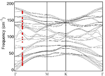
To perform these calculations we had to improve the sampling of the Brillouin zone close to the Fermi surface which is particularly important to resolve a possibly existing anomaly. Given the
peculiar shape of the Fermi surface in the Bi2Se3(111) slabs consisting of a ring around the -point, we used a graded -point mesh (equivalent to a uniform mesh) near the -point point and a coarser one (equivalent to a mesh) near the zone boundary. The results are reported in Figure S1. A one to one comparison between phonon modes calculated with and without SOC shows that there is no evidence of a Kohn anomaly induced by the presence of the surface metallic states, involving any of the surface phonon modes. The spin-orbit coupling results merely in a overall softening of the phonon modes of at most 6%.
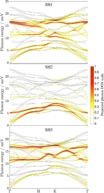
In addition to the shear vertical and shear horizontal phonon densities shown in the main part of the article, Figure S2 shows the shear horizontal polarisations projected onto the first, second and third layer (SH1, SH2, SH3). If the scattering plane, defined by the incoming and scattered He beam, coincides with a mirror plane of the surface, the detection of purely SH modes is in principle forbidden due to symmetry reasonsTamtögl et al. (2015) and we show the calculations of the SH modes here for completeness. However, phonon modes often exhibit a mixing of polarisation components and even a purely SH mode may give rise to charge density oscillations above the first atomic layer which are eventually observed in inelastic He atom scattering.
S2 HAS diffraction scans
Despite the diffraction scans along which are already shown in the main part of the article, Figure S3 shows also a diffraction scans along the azimuth. Note that along there is no evidence for additional peaks close to the diffraction peaks, despite two small features close to the specular reflection which can be assigned to resonancesRuckhofer et al. (2019). This is indicate of the hexagonal shape of the quantum well states giving rise to a multitude of connecting vectors with similar momentum transfer between the flat sides of the hexagon and thus along the azimuth.
S3 TOF Measurements and Surface Phonon Dispersion
The phonon energies were determined by performing time-of-flight (TOF) measurements over a wide range of incident angles between the first-order diffraction peaks and at various beam energies. The phonon dispersion was then obtained by calculating the parallel momentum transfer for each extracted phonon energy from the conservation laws of energy and parallel momentum providing the so-called scan curve for planar scattering:Tamtögl et al. (2013); Safron (1996)
| (S4) |
where is the energy of the incident beam, is the parallel component of the incident wavevector, and and are the incident and final angle, respectively.
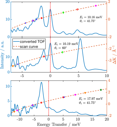
Figure S4 shows some further examples of measured TOF spectra along the azimuth and the sample at room temperature. Each TOF spectrum consists of various peaks which are located on the creation (negative -axis, ) as well as the annihilation (positive -axis, ) side. The peak at zero energy transfer corresponds to elastically scattered helium atoms due to the diffuse elastic peak which is caused by scattering from surface imperfections such as stepsFarías and Rieder (1998); Tamtögl et al. (2018). The scan curve associates each phonon event with a specific momentum transfer based on (Equation S4), since the incoming helium atom looses or gains momentum via inelastic scattering from a phonon.
Figure S4 shows an additional set of TOF-spectra along the direction. Most measurements covering the low energy region with the acoustic phonon modes where performed with a beam (top and centre panel in Figure S4), while for the optical phonon modes higher incident beam energies (bottom panel in Figure S4) where used, in order to cover the optical energy region on the creation side. Note that the particularly strong peak at around in the centre panel is not assigned to a phonon event. This seemingly inelastic feature originates from elastic scattering and is caused by the outer tails of the velocity distribution in the incident beam. These so-called deceptons or spurions occur within the vicinity of the diffraction peaks and give rise to a large intensity in the inelastic spectra due to their elastic nature.Allison et al. (1981).
As mentioned in the main part of the article, there is no evidence for a strong Kohn anomaly (KA) in our measurements as reported by Zhu et alZhu et al. (2011, 2012), who observed a strong V-shaped indentation at for an optical phonon branch originating at meV at the -point. The scan curve on the phonon annihilation side (blue curve) in Figure S5(a) covers exactly the close to the -point. Neither the DFPT calculations (grey lines in Figure S5(a)) support such a KA nor does the experimental data which in turn even shows a minimum of the scattered inelastic intensity in the region of the side (Figure S5(b)).