Probing defect states in few-layer MoS2 by conductance fluctuation spectroscopy
Abstract
Despite the concerted effort of several research groups, a detailed experimental account of defect dynamics in high-quality single- and few-layer transition metal dichalcogenides remain elusive. In this paper we report an experimental study of the temperature dependence of conductance and conductance-fluctuations on several few-layer MoS2 exfoliated on hexagonal boron nitride and covered by a capping layer of high- dielectric HfO2. The presence of the high- dielectric made the device extremely stable against environmental degradation as well as resistant to changes in device characteristics upon repeated thermal cycling enabling us to obtain reproducible data on the same device over a time-scale of more than one year. Our device architecture helped bring down the conductance fluctuations of the MoS2 channel by orders of magnitude compared to previous reports. The extremely low noise levels in our devices made in possible to detect the generation-recombination noise arising from charge fluctuation between the sulphur-vacancy levels in the band gap and energy-levels at the conductance band-edge. Our work establishes conduction fluctuation spectroscopy as a viable route to quantitatively probe in-gap defect levels in low-dimensional semiconductors.
Following the discovery of graphene Novoselov et al. (2004), the exploration of the basic physics and technological implications of two-dimensional (2D) materials has gained tremendous importance. Though graphene is a system rich in novel physics, the lack of band-gap limits its applications in transistor technology. Transition metal dichalcogenides (TMD) like MoS2 and MoSe2, on the other hand, have band-gaps of the order of eV in the few-layer limit Mak et al. (2010) making them ideal for opto-electronic applications Wang et al. (2012); Radenovic et al. (2011); Eda and Maier (2013). On the flip-side, the reported mobilities of these TMD based field effect transistor (FET) devices are very low Li et al. (2014); Radenovic et al. (2011) and the quoted values vary widely between samples. It is now understood that defect-levels (primarily arising from chalcogenide vacancies) adversely affect the mobilty and optical properties of these TMD-based devices Hong et al. (2015); Ong and Fischetti (2013); Qiu et al. (2013); Zhu et al. (2014).
Despite extensive research, there is no clear understanding of the underlying defect dynamics in this system. Traditional transport measurements like current-voltage characteristics and the temperature dependence of the resistance, while providing indications of the existence of defect states, cannot directly probe their energetics Qiu et al. (2013); McDonnell et al. (2014). Photoluminescence measurements report the appearance, at low temperatures of an additional peak in the spectrum which is tentatively attributed to transitions from a ‘defect’-level Tongay et al. (2013); Saigal and Ghosh (2016), but no direct evidence of this level has been found from optical studies. Transmission electron microscopy (TEM) Hong et al. (2015); Lin et al. (2014); Zou et al. (2012); Van Der Zande et al. (2013); Najmaei et al. (2013) and scanning tunnelling microscopy (STM) Hosoki et al. (1992); Permana et al. (1992); Ha et al. (1994); Murata et al. (2001); Kodama et al. (2010); Addou et al. (2015) have shown that the primary point-defects are -vacancies although other types of defects like interstitials, dislocations, dopants and grain boundaries were also seen. These two techniques come with their own sets of limitations. While TEM imaging is believed to induce additional defects in MoS2 Komsa et al. (2012, 2013), atomic-resolution imaging of few-layer TMD using STM has proved challenging McDonnell et al. (2014); Lu et al. (2014); Huang et al. (2015); Vancsó et al. (2016). Thus, although theoretical studies predict the presence of prominent defect-levels in these materials KC et al. (2014); Naik and Jain (2018); Krivosheeva et al. (2015); Lin et al. (2016); Noh et al. (2014), probing them experimentally has proved to be challenging.
In this paper, we present conductance fluctuation spectroscopy Dutta and Horn (1981) as a viable technique to identify these defect states and their characteristic energy levels. Conductance fluctuations (noise) in TMD-based devices has been studied by several groups Song et al. (2017); Kwon et al. (2014); Sangwan et al. (2013); Ghatak et al. (2014); Renteria et al. (2014). In different studies, the observed conductance fluctuations have been variously attributed to charge-carrier number density fluctuations due to trapping at the interface Kwon et al. (2014), to mobility fluctuations Sangwan et al. (2013); Ghatak et al. (2014) or to contact noise Renteria et al. (2014). In general, in the high doping regime, carrier-number density fluctuation model could explain the measured noise behavior while in the low doping regime mobility fluctuation models seemed to better fit the experimental observations Na et al. (2014). Thus there is a lack of consensus in the community as to the origin of the observed large conductance fluctuations in this system. The problem is aggravated by the fact that ultra-thin layers of TMD degrade extremely fast when exposed to the ambient Renteria et al. (2014); Qiu et al. (2012); Late et al. (2012); Kooyman and van Veen (2008). This makes repeated, reliable measurements on the same device challenging while at the same time severely limiting the scope of practical applications.
We have performed detailed measurements of temperature dependence of conductance and conductance-fluctuations on several few-layer MoS2 exfoliated on hexagonal boron nitride (hBN) andcovered by a film of high- dielectric HfO2. We find that over a large range of , the noise in the system is dominated by generation-recombination processes caused by random charge fluctuations via transitions between the -vacancy impurity band and the conduction band of MoS2. Thepresence of the HfO2 capping-layer makes it extremely stable against degradation upon exposure to the atmosphere and to repeated thermal-cycling. The presence of the crystalline hBN beneath screens the device from charge-fluctuations in the SiO2 substrate resulting in the noise levels in our device being orders of magnitude smaller than previous reports of on-substrate devices. This enabled us to detect charge fluctuations between the -vacancy levels and the conduction-band edge.
Samples were prepared in FET configuration by conventional Polydimethylsiloxane (PDMS) assisted dry-transfer method Dean et al. (2010). We studied two classes of devices. In the first class, a few-layer hBN flake ( nm thick) was transferred on Si++/SiO2 substrate followed by the transfer of a few-layer MoS2 on top. The transfers were made using a custom-built set-up based on a motorized XYZ-stage (Thorlabs model B51x) using a long working distance 50X-objective under an optical microscope. Electrical contacts were defined by standard electron-beam lithography followed by thermal deposition of 5 nm Cr and 25 nm Au. This was followed by an electron-beam assisted evaporation of 30 nm of HfO2 covering the entire surface of the device. The HfO2 thin film was deposited directly on MoS2 without any buffer layer or surface treatment - the details of the HfO2 film growth are discussed elsewhere Lakshmi Ganapathi et al. (2013); Ganapathi et al. (2014). Several such devices were tested. In this article we concentrate on the results obtained on one such device, labeled D1. For comparison, we also studied a second class of devices - these were few-layer MoS2 devices fabricated directly on the Si++/SiO2 substrate without the top encapsulation layer (labeled D2). The thickness of the SiO2 in all cases was 295 nm. In all cases, the gate bias voltage, is applied from underneath Si++/SiO2 substrate.
Electrical transport measurements were performed in a two-probe configuration using low-frequency lock-in technique. The bias voltage across the device was set to 5 mV. The current flowing through the device was amplified by a low-noise current-amplifier (Ithaco 1211) and measured by a digital dual-channel Lock-in-amplifier (LIA). The gate voltage, was controlled by a Keithley-2400 source-meter.
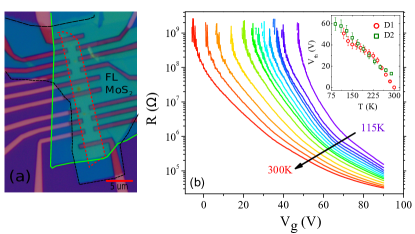
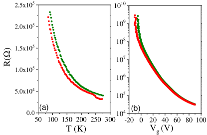
An optical image of the device D1 is shown in Fig. 1(a), the few-layer MoS2 (encapsulated between hBN and HfO2) is outlined by a black dashed line. Fig. 1(b) shows a plot of the sheet resistance of the device D1 versus measured over the temperature range 115–300 K. The gate response of the device establishes it to be an n-type semiconductor which is typically what is observed in naturally occurring MoS2. The large on-off ratio (), low on-state resistance ( K) and very low off-state current (10 pA) attest to the high-quality of the device. From the inset of Fig. 1(b) it can be seen that the threshold voltage decreases sharply with increasing temperature going to negative near room-temperature. On the other hand, for D2 at room temperature was V.
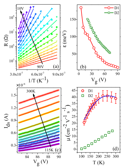
In Fig. 2(a) we plot the sheet resistance of the device D1 in a semi-logarithmic scale versus inverse temperature for few representative values of . The linearity of the plots indicates that, at least in the high limit, electrical transport is dominated by thermal activation of the charge carriers. More specifically, as we go higher in , the range of where this linearity holds extends down to lower temperatures. The activation energy, extracted from the slope of the versus plots is plotted in Fig. 2(b). One can see that increases as one decreases the gate bias and it varies from 20 meV at high to an order of magnitude higher 200 meV, close to the off-state of the device. The activation energy for device D2, extracted in a similar fashion is, as expected, higher than that of D1 at all values of .
The field-effect mobility of the devices can be obtained from the relation . Here is the length of the channel, its width and is the gate capacitance per unit area. In Fig. 2(c) we show plots of versus , the slope of this curve gives the mobility of the device. A plot of the dependence of the mobility is shown in Fig. 2(d). We find that for device D1 is cm-2V-1s-1 at 100 K. With increasing , increases monotonically till about 225 K beyond which it begins to fall with increasing . To understand the measured dependence of we note that in 2D semiconductors, the mobility of the charge carriers is affected by Coulomb scattering, acoustic and optical phonon scattering, scattering by the interface phonon and roughness due to the surface Kim et al. (2012). At high–, scattering due to phonons is dominant which causes the mobility to have a dependence Sangwan and Hersam (2018); Mao et al. (2017). On the other hand, scattering from charge impurities located randomly in the sample is the dominant factor limiting at low temperatures causing the mobility to depend on temparature as Ong and Fischetti (2013); Liu et al. (2017). Following Matthiessen’s rule:
| (1) |
where and represent the relative contributions of the phonon-scattering and impurity-scattering mechanisms respectively. These coefficients are not independent, but are related by , where is the temperature at which has a maxima. In Fig. 2(d) we show a fit of the dependence of the mobility of D1 to Eqn. 1. The mobility of D2, on the other hand, monotonically increases with showing that over the range of studied, impurity-scattering dominates the transport in on-SiO2 substrate devices.
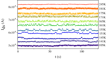
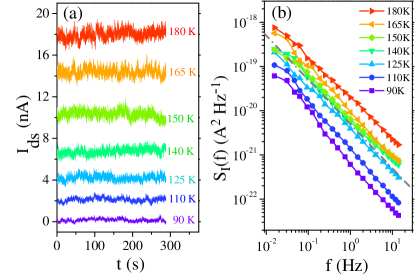
The presence of both bulk- and surface-transport channels complicates the charge transport in these systems. To understand the charge-carrier dynamics arising from the surface- and bulk-states in this system, we studied the low-frequency conductance fluctuations over the temperature range 70 K-300 K using a 2-probe ac digital-signal-processing technique Bid (2006). As established in several previous reports, noise is an excellent parameter to probe inter-band scattering of charge-carriers in systems with multiple conduction channels Daptary et al. (2018); Price (1981); Hooge (1994). We used an SR830 dual-channel digital LIA to voltage-bias the sample at a carrier frequency of . The current through the device was amplified by the low-noise current preamplifier and detected by the LIA. The data were acquired at every and for 32 minutes at a sampling rate of 2048 points/s using a fast 16-bit data acquisition card. This time-series of current fluctuations was digitally anti-alias filtered and decimated. The power spectral density (PSD) of current-fluctuations, was calculated from this filtered time-series using the method of Welch-periodogram Bid (2006); Scofield (1987). The system was calibrated by measuring the thermal (Johnson-Nyquist) noise of standard resistors. The time-series of measured for device D1 at a few representative temperatures at V are shown in Fig. 3. We find that over the range 140-190 K, the measured (and consequently the conductance ) for D1 fluctuates between two well-defined levels Du Pré (1950); Kundu et al. (2017). This ‘Random telegraphic noise’ (RTN) Hung et al. (1990) usually signifies that the system has access to two (or more) different states separated by an energy barrier. We come back later in this article to a discussion of the detailed statistics of the RTN and the physical origin of these states.
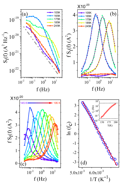
In Fig. 4(a) we plot the PSD of current fluctuations at a few representative values of and V for the device D1. We find that over the range where RTN were present in the time-series , the PSD deviates significantly from the dependence (shown in the plot by a gray line). This can be appreciated better from Fig. 4(b) where we plot the quantity which should be independent of frequency for noise, as is indeed the case for the PSD measured at 105 K and 245 K. On the other hand, the PSD measured in the intermediate range ( K K) has a significant non- component. The PSD of an RTN is a Lorentzian with a characteristic frequency , where is the typical time-scale of switching between the two distinct levels. This motivated us to fit the measured PSD of current fluctuations to an equation which contains both and Lorentzian components:
| (2) |
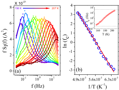
and are fit parameters that denote the relative contributions of the random and RTN fluctuations respectively to the total PSD. The dotted purple lines are fits to the data at 165 K, 175 K and 185 K using Eqn. 2. In Fig. 4(c) we show plots of versus over an extensive range of . We find that as increases, the peak position evolves from a few mHz to few tens of Hz [see the inset of Fig. 4(d). Beyond this range, the value of goes beyond our measurement frequency bandwidth (31.25 mHz–28 Hz). The value of is thermally activated and follows the Arrhenius relation: = . Figure 4(d) shows a plot of ln() versus , the red-line is a fit to the activated behaviour. The value of activation energy extracted from the fit is 370 meV. These measurements were repeated on three such devices (MoS2 encapsulated between hBN and HfO2); we find that the activation energy-scale in all of them lie in the range meV. In Fig. 5, we show data for another device, D1b, for which we obtain =353 meV. We come back to the physical implications of this energy-scale later in this article.
The time-series for device D2, on the other hand, did not have any RTN component (Fig. 6(a)) and the PSD had a (with ) dependence on over the entire and range studied (Fig. 6(b)). The (t) data were obtained for the device D2 at 72 V. We have attempted to compare the data in the two sets of devices at similar values of number-densities. Due to the presence of the hBN layer, the effective thickness of the dielectric layer in D1 was higher than that of D2 – requiring a higher gate-voltage for D1 than that for D2 to achieve similar carrier number density. On the other hand, D1 had a lower threshold voltage than D2. Taking both these factors into account, we have estimated the at which the induced number densities are similar for both D1 and D2. Thus, for D1, the data are presented for =90 V while for the device D2, the data are presented for = 72 V.
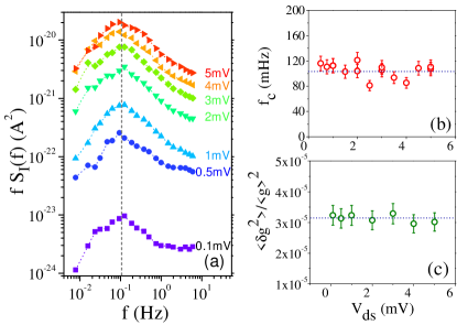
In Fig. 7(a) we present the dependence of the quantity measured at = 175 K and = 90 V for the device D1. We see that the form of the PSD is independent of . To make this observation quantitative, we plot in Fig. 7(b) the dependence of on extracted from these plots using Eqn. 2. The fact that is independent of within experimental uncertainties shows that this time-scale is intrinsic to the sample Hooge et al. (1981).
The PSD, can be integrated over the frequency bandwidth of measurement to obtain the relative variance of conductance fluctuations, at a fixed and :
| (3) |
The relative variance of conductance fluctuations, was found to be independent of at all and confirming that the noise arises from conductance fluctuations in the MoS2 channel and not from the contacts [for representative data, see Fig. 7(c)].
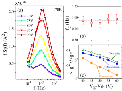
We measured the noise as a function of gate-bias voltage, – the results obtained at = 170 K for the device D1 are plotted in Fig. 8(a). We find to be independent of (Fig. 8(b)) with-in experimental uncertainties. In Fig. 8(c) we have plotted as a function of -. The total noise has been separated into its -component and the RTN-component. At low values of -, the -component noise contribution is comparable to that of the RTN-component while at higher -, the RTN-component dominates the measured conductance fluctuations. This motivated us to perform our noise measurements at high (90 V) so that the RTN component of the noise is easily resolvable.
In Fig. 9 we show a plot of versus for the two devices. The noise-data for device D1 (plotted in green open circles) has a prominent hump over the range (140–190 K) coinciding with the regime where we observed RTN. To appreciate this, we plot on the same graph the relative variance of conductance fluctuations arising from the component (red filled circles) as well as the Lorentzian component (blue open circles). It can be seen that the increase in noise over the 140–190 K temperature range is entirely due to two-level conductance fluctuations in the system. For comparison, we also add a plot of versus for the unencapsulated device prepared on SiO2-substrate, D2. The noise on SiO2 substrate devices, is more than two orders of magnitude larger than that of D1 and matches with previous reports of measured noise in MoS2 by various groups Renteria et al. (2014); Sangwan et al. (2013). Our work thus shows that encapsulation helps in significantly improving the signal to noise ratio.
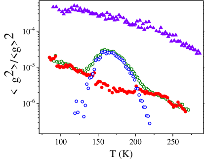
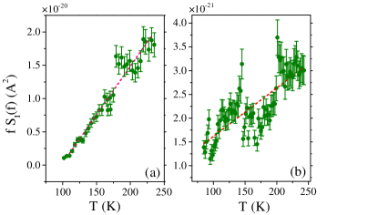
A careful study of Fig. 9 provides clues to the origin of the observed noise in this system. The temperature dependence of the relative variance of conductance fluctuations () measured for the on-SiO2 substrate device D2 closely resembles the -dependence of the component of measured on D1. This indicates that these two noises have similar origins. The primary source of the -dependence of noise in many semiconductor devices is generation-recombination (GR) noise due to trapping-detrapping of charges at the gate dielectric-channel interfaces. This process can be quantified by the McWhorter model McWhorter (1957); Ghibaudo et al. (1991); Na et al. (2014):
| (4) |
where is the areal-density of trapped charges per unit energy, and are respectively the width and the length of the device-channel, is the gate-capacitance per unit area. is the Boltzmann constant and is the charge of the electron. Equation 4 predicts the linear dependence of on the temperature. Fig. 10 shows a plot of versus for both D1 and D2. The plots are linear to within experimental uncertainties. From the slopes of these plots, the value of for device D2 was extracted to be cm-2 eV-1 which agrees with previously reported values for MoS2 devices prepared on SiO2 substrates Dubey et al. (2017). On the other hand, for the HfO2 covered, on-hBN device D1, cm-2 eV-1, more than two orders of magnitude lower than that in the on-SiO2 substrate device D2.
The non- seen only in the encapsulated device has a different origin. The presence of RTN in the time-series of conductance fluctuations and the associated Lorentzian component in the PSD indicates that the noise originates from random charge fluctuations via transitions between two well-defined energy states separated by an energy barrier. We propose that in this case, these two levels correspond to the -vacancy impurity band and the conduction band. This is supported by the fact that the value of the activation energy, meV extracted from the temperature dependence of the corner-frequency of the Lorentzian component of the current fluctuations matches closely with the estimated position of the -vacancy impurity band with respect to the conduction band edge Ghorbani-Asl et al. (2013). Note that it was possible for us to detect this fluctuation-component only because of the two orders of noise reduction made possible by the introduction of hBN between the MoS2 and SiO2 substrate.
The HfO2 layer has a two-fold effect on the noise. Firstly, being a high-k dielectric with a dielectric constant value of about 25, its presence screens the device from Coulomb scattering, and reduces the noise by orders of magnitude, enabling us to detect the RTN. Secondly, it acts as a capping layer that shields the MoS2 from the ambient. We believe that this prevents the -vacancies from getting saturated by adsorbates, thus preserving the RTN. With the current data, we cannot distinguish between these two effects. Preliminary results obtained on devices fabricated on hBN without the HfO2 capping layer had higher on-off ratios, higher-mobilities and lower noise levels as compared to MoS2 devices fabricated on SiO2 without the HfO2 capping layer - however, we did not find any RTN in these devices. From these results, one can tentatively conclude that both the top- and bottom-layers are necessary to preserve the RTN. This issue is currently under detailed investigation.
Finally, coming to the question of stability of the devices, we have compared the versus , versus and the noise measurements on device D1 immediately after fabrication and after a gap of several months. The sample was thermally cycled several times during this period between 300 K and 77 K. As shown in Fig. 11, the temperature and dependence of the resistance of the device were quite reproducible. This is in sharp contrast to unencapsulated on-SiO2 devices like D2 in which after a few days the channel and contacts both degrade drastically making further measurements impossible Renteria et al. (2014). Similarly, thermal cycling alters the characteristics of such devices and makes the channel resistance unstable. The stability of the resistance of D1 over time period of months confirms that encapsulation between hBN and HfO2 makes the device robust to thermal cycling and against degradation with time.
To conclude, in this paper we reported on detailed conductance fluctuation spectroscopy of high-quality MoS2 devices encapsulated between hBN and HfO2. The presence of the high- dielectric made the device extremely stable against environmental degradation enabling us to obtain reproducible data on the same device for over 1 year. The hBN substrate helped bring down the conductance fluctuations by over two orders of magnitude as compared to similar devices on bare SiO2 substrates. The low noise levels in our devices made it possible to detect the generation-recombination noise arising from charge fluctuation between the -vacancy levels in the MoS2 band-gap and states at its conductance band edge. Our work establishes conduction fluctuation spectroscopy as a viable route to detect in-gap defect levels in low-dimensional semiconductors.
Acknowledgements.
AB acknowledges funding from Nanomission and FIST program, Department of Science & Technology (DST), government of India and the Indo-French Centre for the Promotion of Advanced Research (CEFIPRA) (Project No. 5304-F).References
- Novoselov et al. (2004) K. S. Novoselov, A. K. Geim, S. V. Morozov, D. Jiang, Y. Zhang, S. V. Dubonos, I. V. Grigorieva, and A. A. Firsov, science 306, 666 (2004).
- Mak et al. (2010) K. F. Mak, C. Lee, J. Hone, J. Shan, and T. F. Heinz, Physical review letters 105, 136805 (2010).
- Wang et al. (2012) Q. H. Wang, K. Kalantar-Zadeh, A. Kis, J. N. Coleman, and M. S. Strano, Nature nanotechnology 7, 699 (2012).
- Radenovic et al. (2011) A. Radenovic, J. Brivio, V. Giacometti, A. Kis, et al., Nat. Nanotechnol 6, 147 (2011).
- Eda and Maier (2013) G. Eda and S. A. Maier, Acs Nano 7, 5660 (2013).
- Li et al. (2014) H. Li, J. Wu, Z. Yin, and H. Zhang, Accounts of Chemical Research 47, 1067 (2014), pMID: 24697842, eprint https://doi.org/10.1021/ar4002312, URL https://doi.org/10.1021/ar4002312.
- Hong et al. (2015) J. Hong, Z. Hu, M. Probert, K. Li, D. Lv, X. Yang, L. Gu, N. Mao, Q. Feng, L. Xie, et al., Nature communications 6, 6293 (2015).
- Ong and Fischetti (2013) Z.-Y. Ong and M. V. Fischetti, Physical Review B 88, 165316 (2013).
- Qiu et al. (2013) H. Qiu, T. Xu, Z. Wang, W. Ren, H. Nan, Z. Ni, Q. Chen, S. Yuan, F. Miao, F. Song, et al., Nature communications 4, 2642 (2013).
- Zhu et al. (2014) W. Zhu, T. Low, Y.-H. Lee, H. Wang, D. B. Farmer, J. Kong, F. Xia, and P. Avouris, Nature Communications 5, 3087 (2014).
- McDonnell et al. (2014) S. McDonnell, R. Addou, C. Buie, R. M. Wallace, and C. L. Hinkle, ACS nano 8, 2880 (2014).
- Tongay et al. (2013) S. Tongay, J. Suh, C. Ataca, W. Fan, A. Luce, J. S. Kang, J. Liu, C. Ko, R. Raghunathanan, J. Zhou, et al., Scientific reports 3, 2657 (2013).
- Saigal and Ghosh (2016) N. Saigal and S. Ghosh, Applied Physics Letters 109, 122105 (2016).
- Lin et al. (2014) Y.-C. Lin, D. O. Dumcenco, H.-P. Komsa, Y. Niimi, A. V. Krasheninnikov, Y.-S. Huang, and K. Suenaga, Advanced materials 26, 2857 (2014).
- Zou et al. (2012) X. Zou, Y. Liu, and B. I. Yakobson, Nano letters 13, 253 (2012).
- Van Der Zande et al. (2013) A. M. Van Der Zande, P. Y. Huang, D. A. Chenet, T. C. Berkelbach, Y. You, G.-H. Lee, T. F. Heinz, D. R. Reichman, D. A. Muller, and J. C. Hone, Nature materials 12, 554 (2013).
- Najmaei et al. (2013) S. Najmaei, Z. Liu, W. Zhou, X. Zou, G. Shi, S. Lei, B. I. Yakobson, J.-C. Idrobo, P. M. Ajayan, and J. Lou, Nature materials 12, 754 (2013).
- Hosoki et al. (1992) S. Hosoki, S. Hosaka, and T. Hasegawa, Applied surface science 60, 643 (1992).
- Permana et al. (1992) H. Permana, S. Lee, and K. S. Ng, Journal of Vacuum Science & Technology B: Microelectronics and Nanometer Structures Processing, Measurement, and Phenomena 10, 2297 (1992).
- Ha et al. (1994) J. S. Ha, H.-S. Roh, S.-J. Park, J.-Y. Yi, and E.-H. Lee, Surface science 315, 62 (1994).
- Murata et al. (2001) H. Murata, K. Kataoka, and A. Koma, Surface science 478, 131 (2001).
- Kodama et al. (2010) N. Kodama, T. Hasegawa, Y. Okawa, T. Tsuruoka, C. Joachim, and M. Aono, Japanese Journal of Applied Physics 49, 08LB01 (2010).
- Addou et al. (2015) R. Addou, L. Colombo, and R. M. Wallace, ACS applied materials & interfaces 7, 11921 (2015).
- Komsa et al. (2012) H.-P. Komsa, J. Kotakoski, S. Kurasch, O. Lehtinen, U. Kaiser, and A. V. Krasheninnikov, Physical review letters 109, 035503 (2012).
- Komsa et al. (2013) H.-P. Komsa, S. Kurasch, O. Lehtinen, U. Kaiser, and A. V. Krasheninnikov, Physical Review B 88, 035301 (2013).
- Lu et al. (2014) C.-P. Lu, G. Li, J. Mao, L.-M. Wang, and E. Y. Andrei, Nano letters 14, 4628 (2014).
- Huang et al. (2015) Y. L. Huang, Y. Chen, W. Zhang, S. Y. Quek, C.-H. Chen, L.-J. Li, W.-T. Hsu, W.-H. Chang, Y. J. Zheng, W. Chen, et al., Nature communications 6, 6298 (2015).
- Vancsó et al. (2016) P. Vancsó, G. Z. Magda, J. Pető, J.-Y. Noh, Y.-S. Kim, C. Hwang, L. P. Biró, and L. Tapasztó, Scientific reports 6, 29726 (2016).
- KC et al. (2014) S. KC, R. C. Longo, R. Addou, R. M. Wallace, and K. Cho, Nanotechnology 25, 375703 (2014).
- Naik and Jain (2018) M. H. Naik and M. Jain, Phys. Rev. Materials 2, 084002 (2018).
- Krivosheeva et al. (2015) A. V. Krivosheeva, V. L. Shaposhnikov, V. E. Borisenko, J.-L. Lazzari, C. Waileong, J. Gusakova, and B. K. Tay, Journal of Semiconductors 36, 122002 (2015).
- Lin et al. (2016) Z. Lin, B. R. Carvalho, E. Kahn, R. Lv, R. Rao, H. Terrones, M. A. Pimenta, and M. Terrones, 2D Materials 3, 022002 (2016).
- Noh et al. (2014) J.-Y. Noh, H. Kim, and Y.-S. Kim, Physical Review B 89, 205417 (2014).
- Dutta and Horn (1981) P. Dutta and P. M. Horn, Rev. Mod. Phys. 53, 497 (1981).
- Song et al. (2017) S. H. Song, M.-K. Joo, M. Neumann, H. Kim, and Y. H. Lee, Nature communications 8, 2121 (2017).
- Kwon et al. (2014) H.-J. Kwon, H. Kang, J. Jang, S. Kim, and C. P. Grigoropoulos, Applied Physics Letters 104, 083110 (2014).
- Sangwan et al. (2013) V. K. Sangwan, H. N. Arnold, D. Jariwala, T. J. Marks, L. J. Lauhon, and M. C. Hersam, Nano letters 13, 4351 (2013).
- Ghatak et al. (2014) S. Ghatak, S. Mukherjee, M. Jain, D. Sarma, and A. Ghosh, APL Materials 2, 092515 (2014).
- Renteria et al. (2014) J. Renteria, R. Samnakay, S. Rumyantsev, C. Jiang, P. Goli, M. Shur, and A. Balandin, Applied Physics Letters 104, 153104 (2014).
- Na et al. (2014) J. Na, M.-K. Joo, M. Shin, J. Huh, J.-S. Kim, M. Piao, J.-E. Jin, H.-K. Jang, H. J. Choi, J. H. Shim, et al., Nanoscale 6, 433 (2014).
- Qiu et al. (2012) H. Qiu, L. Pan, Z. Yao, J. Li, Y. Shi, and X. Wang, Applied Physics Letters 100, 123104 (2012).
- Late et al. (2012) D. J. Late, B. Liu, H. S. S. R. Matte, V. P. Dravid, and C. N. R. Rao, ACS Nano 6, 5635 (2012), pMID: 22577885.
- Kooyman and van Veen (2008) P. J. Kooyman and J. R. van Veen, Catalysis Today 130, 135 (2008).
- Dean et al. (2010) C. R. Dean, A. F. Young, I. Meric, C. Lee, L. Wang, S. Sorgenfrei, K. Watanabe, T. Taniguchi, P. Kim, K. L. Shepard, et al., Nature nanotechnology 5, 722 (2010).
- Lakshmi Ganapathi et al. (2013) K. Lakshmi Ganapathi, N. Bhat, and S. Mohan, Applied Physics Letters 103, 073105 (2013).
- Ganapathi et al. (2014) K. L. Ganapathi, N. Bhat, and S. Mohan, Semiconductor Science and Technology 29, 055007 (2014).
- Kim et al. (2012) S. Kim, A. Konar, W.-S. Hwang, J. H. Lee, J. Lee, J. Yang, C. Jung, H. Kim, J.-B. Yoo, J.-Y. Choi, et al., Nature communications 3, 1011 (2012).
- Sangwan and Hersam (2018) V. K. Sangwan and M. C. Hersam, Annual review of physical chemistry 69, 299 (2018).
- Mao et al. (2017) J. Mao, J. Shuai, S. Song, Y. Wu, R. Dally, J. Zhou, Z. Liu, J. Sun, Q. Zhang, C. dela Cruz, et al., Proceedings of the National Academy of Sciences 114, 10548 (2017).
- Liu et al. (2017) C. Liu, K. Huang, W.-T. Park, M. Li, T. Yang, X. Liu, L. Liang, T. Minari, and Y.-Y. Noh, Materials Horizons 4, 608 (2017).
- Bid (2006) A. Bid, Ph.D. thesis, Indian Institute of Science (2006).
- Daptary et al. (2018) G. N. Daptary, P. Kumar, A. Dogra, and A. Bid, Physical Review B 98, 035433 (2018).
- Price (1981) P. Price, Annals of Physics 133, 217 (1981).
- Hooge (1994) F. Hooge, IEEE Transactions on Electron Devices 41, 1926 (1994).
- Ghosh et al. (2004) A. Ghosh, S. Kar, A. Bid, and A. Raychaudhuri, arXiv preprint cond-mat/0402130 (2004).
- Scofield (1987) J. H. Scofield, Review of scientific instruments 58, 985 (1987).
- Du Pré (1950) F. K. Du Pré, Phys. Rev. 78, 615 (1950).
- Kundu et al. (2017) H. K. Kundu, S. Ray, K. Dolui, V. Bagwe, P. R. Choudhury, S. Krupanidhi, T. Das, P. Raychaudhuri, and A. Bid, Physical review letters 119, 226802 (2017).
- Hung et al. (1990) K. K. Hung, P. K. Ko, C. Hu, and Y. C. Cheng, IEEE electron device letters 11, 90 (1990).
- Hooge et al. (1981) F. Hooge, T. Kleinpenning, and L. Vandamme, Reports on progress in Physics 44, 479 (1981).
- McWhorter (1957) A. H. McWhorter, Semiconductor surface physics, 207 (Univ. of Pennsylvania Press, 1957).
- Ghibaudo et al. (1991) G. Ghibaudo, O. Roux, C. Nguyen-Duc, F. Balestra, and J. Brini, physica status solidi (a) 124, 571 (1991).
- Dubey et al. (2017) S. Dubey, S. Lisi, G. Nayak, F. Herziger, V.-D. Nguyen, T. Le Quang, V. Cherkez, C. González, Y. J. Dappe, K. Watanabe, et al., ACS Nano 11, 11206 (2017), pMID: 28992415.
- Ghorbani-Asl et al. (2013) M. Ghorbani-Asl, A. N. Enyashin, A. Kuc, G. Seifert, and T. Heine, Physical Review B 88, 245440 (2013).