First principle investigation of hydrogen behavior in M doped Cu2O (M Na, Li and Ti)
Abstract
We study the hydrogen effect on the electronic, magnetic and optical properties of Cu2O in presence of different dopants (Na, Li and Ti). The electronic properties calculations show that hydrogen changes the conductivity of Cu2O from p to n-type. The results show that interstitial hydrogen atom prefers to locate in the tetrahedral site in Cu2O system and it decreases the band gap value of the later. The Na or Li doping Cu2O preserves the p-type conductivity of Cu2O, while hydrogen is the source of n-type conductivity in Na or Li doped Cu2O systems. Ti doping increases the band gap value of Cu2O and makes it an n-type semiconductor. Hydrogen increases the optical transmittance of M doped Cu2O.
Key words: Cu2O, hydrogen, density functional theory
PACS: 70.
Abstract
Äîñëiäæóєòüñÿ âïëèâ âîäíþ íà åëåêòðîííi, ìàãíiòíi òà îïòèчíi âëàñòèâîñòi Cu2O ó ïðèñóòíîñòi ðiçíèõ ëåãóþчèõ äîìiøîê (Na, Li i Ti). Ðîçðàõóíêè åëåêòðîííèõ âëàñòèâîñòåé ïîêàçóþòü, ùî âîäåíü çìiíþє ïðîâiäíiñòü Cu2O ç p äî n-òèïó. Ðåçóëüòàòè ïîêàçóþòü, ùî ìiæâóçëîâèé àòîì âîäíþ âîëiє ðîçòàøóâàòèñÿ â òåòðàåäðèчíié äiëÿíöi â ñèñòåìi Cu2O i çìåíøóє øèðèíó çàáîðîíåíî¿ çîíè îñòàííüî¿. Cu2O, ëåãîâàíèé Na àáî Li çáåðiãàє p-òèï ïðîâiäíîñòi Cu2O, â òîé чàñ ÿê âîäåíü є äæåðåëîì n-òèïó ïðîâiäíîñòi â ñèñòåìàõ Cu2O, ëåãîâàíèõ Na àáî Li. Ti ëåãóâàííÿ çáiëüøóє øèðèíó çàáîðîíåíî¿ çîíè Cu2O i ðîáèòü ¿¿ íàïiâïðîâiäíèêîì n-òèïó. Âîäåíü ïiäâèùóє êîåôiöiєíò îïòèчíîãî ïðîïóñêàííÿ Ì-ëåãîâàíîãî Cu2O.
Ключовi слова: Cu2O, âîäåíü, òåîðiÿ ôóíêöiîíàëó ãóñòèíè
1 Introduction
Owing to high optical absorption coefficient, non-toxicity, abundancy and inexpensive layer formation, copper oxide (CuxO) is appealing to a renewed and rising interest. It could have a potential role in fabricating semiconductor devices, among others, for nanoelectronic, spintronic and photovoltaic applications [1, 2, 3]. We know copper oxide as a p-type semiconductor in two stable forms, cupric oxide (CuO) and cuprous oxide (Cu2O) and this latter enables higher conversion efficiency when used as an absorber material for solar cell applications [4, 5]. Moreover, the possibility of synthesizing nanoparticles enables excellent properties and opens the way to a new class of innovative and more efficient devices [6]. The ability to control the conductivity type can be important for the synthesizing of Cu2O thin films paired with other p-type materials. The challenge of p-type doping of Cu2O must take hydrogen into account, since it is known to passivate any acceptors in solar cell absorbers [7] and reverse the polarity of conductivity in other materials [8]. Hydrogen is present in all semiconductors, including oxides, and is highly reactive, forming a complex with most impurities and defects in the lattice. Hydrogen is a potential source of n-type conductivity [9, 10, 11]. The capability of hydrogen to remove or stimulate the electrical and optical activity of impurities makes it sometimes a helpful, sometimes a disagreeable agent, in either case. However, a theoretical understanding of the principal interactions is very important. The diversity and complexity of hydrogen states, inside the lattice and in traps, has made their characterization impossible by experimental methods alone; the complementary role of theory is proved to be essential [12]. The earlier calculations suggested that interstitial hydrogen prefers to locate in the bond center site (BC) in CdTe and ZnO lattices [13, 14, 15, 16]. It could locate in the tetrahedral site in other oxides such SnO2 and TiO2 [17, 18]. Theoretical prediction and spectroscopy confirmed that hydrogen in semiconductors may be a cause of n-type conductivity; it forms shallow-donor states in the zinc oxide (ZnO) [13, 19, 20, 21]. Peacock and Robertson [22] showed that hydrogen acts as a shallow donor in many oxides, while deep in the silicates, SiO2 and Al2O3. Scanlon and Watson [23] studied the behavior of hydrogen in p-type Cu2O; they showed that hydrogen could weaken the performance of Cu2O solar cell devices. It is important, however, to study the H atom influence on different properties of Cu2O and M doped Cu2O (M= Na, Li, Ti). As the fabrication process of solar cell devices uses different kind of gas, the knowledge of the hydrogen effect is important in choosing the gas in the annealing process.
Our work uses the first-principles calculations. We study the effect of hydrogen on the electronic, magnetic and optical properties of Cu2O and Cu2(1-x)MxO. To find the favoured position of the hydrogen atom in the systems studied, we calculated the formation energies of different configurations proposed. In addition, we try to discuss the influence of hydrogen and different dopants on physical properties of M doped Cu2O. We also predict and give an easy, low-cost, and scalable strategy to prepare the Cu2O composite on heterostructure solar cells, hydrogen storage and/or production.
2 Computational details
We used ab initio total-energy and molecular-dynamics program VASP (Vienna ab initio simulation program) developed at the Fakultät für Physik of the Universität Wien [24, 25], to do all calculations. For treatment of the exchange and correlation energies, we used the generalized gradient approximation (GGA) [26] with projector-augmented wave (PAW) [25, 27] pseudo-potentials. Brillouin zone integrals are converged with a 450 eV plane-wave cut-off, and a Monkhorst-Pack k-point mesh suffices to make sure that energy convergence takes place for supercell. These calculations showed a discrepancy within 10-7 eV. We performed a relaxation with the standard conjugated gradient algorithm. We used the supercell approach to simulate the H doped Cu2O or (Cu2, M)O system. The optimized lattice constant of Cu2O, Å, is in good agreement with the experimental value of Å [28, 29] and theoretical values and 4.20 Å [30, 31].
In these calculations, we positioned the M atoms at the cation sites (Cu). We performed the H defect formation energy calculations on supercell, containing 162 atoms, using the calculated lattice constant with the defect at different positions in the cell. The supercell size is necessary to allow for a detailed study of many different dopant geometric structures. For calculations of the electronic properties of H doped (Cu2, M)O, we suppose that M atom leads to the formation of supercell with chemical composition Cu2(107)MO54, with one atom of hydrogen at the interstitial site. All calculations were spin polarized. We can determine optical properties using the complex dielectric function [32]. The imaginary part of the dielectric function was calculated from the momentum matrix elements between the occupied and unoccupied wave functions [33]:
| (2.1) |
Here, are the volume of cell, conduction band, valence band, point, photon frequency, external field vector, respectively, while and represent the eigenstates. We can obtain the real part of the dielectric function, from by the Kramer–Kronig relationship [34]. The corresponding absorption coefficient was obtained using the following equation:
| (2.2) |
3 Results and discussion
3.1 Hydrogen in Cu2O
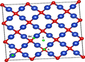
In Cu2O lattice we can attribute different substitutional and interstitial positions to hydrogen impurity. Figure 1 illustrates all positions where copper, oxygen and hydrogen atoms are, respectively, represented by blue, red and green spheres. In this figure, we notice four possible sites for the hydrogen impurity, T (Tetrahedral site), BC (Bond Center site), C (Cation substitutional site) and A (Anion substitutional site).
To find the preferred site of H in Cu2O, we calculated the formation energies for all hydrogen positions. We show the obtained results in table 1. The references [35, 36] give the formation energy for hydrogen insertion in Cu2O as follows:
| (3.1) |
In case of substitution, the formation energy associated is:
| (3.2) |
| (3.3) |
is the total energy of supercell with one hydrogen atom, is the total energy of supercell without defects , and are the total energies of an isolated hydrogen, cuprous and oxygen atoms, respectively, in the ground state. The last term in the formation energy () accounts because H+ donates an electron , and H- accepts an electron . is the Fermi level energy. If the formation energy is positive , the implantation of the hydrogen atom into the Cu2O lattice is energetically unfavorable.
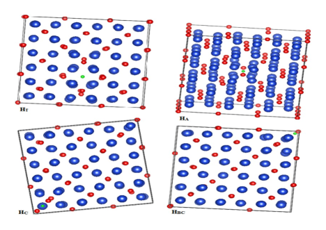
One can see from table 1 that the lowest formation energy is that of the T site with eV. These values show that hydrogen prefers to localize in the tetrahedral site in Cu2O lattice, which confirms earlier results [23, 37]. Figure 2 shows different configurations of hydrogen in Cu2O relaxed lattice. We can see that with insertion in the tetrahedral site, anionic site and cationic site, the hydrogen position does not change, while with insertion in Cu-O bond center, the hydrogen atom takes another position in the Cu2O lattice.
| Sites | H | H | H | H |
|---|---|---|---|---|
| (eV) | – 0.77 | 5.64 | 0.15 | 0.41 |
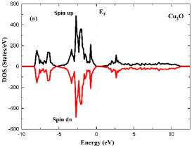
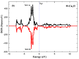
We plotted the total densities of state (TDOS) of pure Cu2O and a single H-doped Cu2O in figure 3. The TDOS figures show that hydrogen causes a change in the position of the Fermi level from near the valence band towards conduction band, leading the system to n-type semiconductor characteristic; this result agrees well with earlier works [23, 38]. In fact, this behavior of hydrogen was found in other p-type oxide materials such as SnO2, TiO2 and ZnO [38, 39, 40, 41]. The calculated band gap of Cu2O, =0.55 eV, is smaller than the experimental value (2.17 eV) [42] according to the DFT-GGA calculations. The result agrees well with the earlier theoretical values reported in the literature (0.6 eV [43, 44], 0.64 eV [45] and 0.7 eV [46]). For hydrogen doped Cu2O, we notice a narrow energy gap of 0.09 eV of the majority-spin electrons, while for the minority-spin electrons, the band gap is 0.23 eV. The hydrogen in Cu2O decreases the band gap value of Cu2O.
To improve the physical properties of Cu2O for voltaic applications, we have tried three different dopants: Sodium (Na), Lithium (Li) and Titanium (Ti). We investigated the properties of M doped Cu2O, M= Na, Li and Ti, by substituting one M atom for one Cu atom in the supercell Cu(108)O54.
In Cu2(1-x)MxO structure, we consider two configurations where interstitial hydrogen atom is at the tetrahedral site. In the first one, a short distance (S) separates M and H while in the second one, a long distance (L) separates M and H atoms.
3.2 Na and H doped Cu2O
In the first case configuration (S), the distance between Na and H was 1.78 Å while after relaxation this distance becomes 2.38 Å. This suggests that H atom relaxes to move away from the Na atom. For the second configuration (L) and before relaxation, the distance between Na and H was 6.98 Å. After relaxation, this distance hardly moves to only 7.012 Å.
We show the total density of states of Na doped Cu2O in figure 4 (a). The figure indicates that the Na doping decreases the band gap of Cu2O. The doping of Cu2O by Na does not change the nature of his conductivity; the calculated energy of the gap is 0.35 eV. Elfadill et al. [47] showed that Na doping Cu2O is a p-type characteristic, which shows that our calculations are in good agreement with experimental data. In addition, Minami et al. used Cu2O doped Na as p-type in p-n heterojunction and/or homojunction solar cells [48, 49].
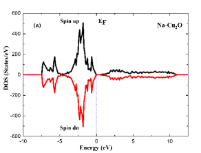
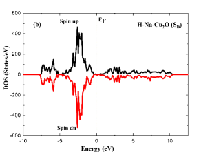
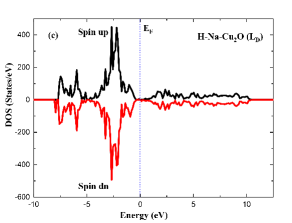
For hydrogen implantation in Na doped Cu2O, the calculated band gap is 0.47 eV for a short distance. In the long distance case, we note two different band gap values, 0.47 eV and 0.35 eV for the majority-spin and minority-spin electron, respectively. From the DOS figures [figure 4 (b), figure 4 (c)], we note that hydrogen changes the position of Fermi level () of Na doped Cu2O, moves from the valence band to conduction band. Thus, Na doped Cu2O becomes n-type semiconductor. The distance between Na and H atoms does not influence the electronic properties of Na doped Cu2O, we found the same band gap value in the two configurations.
3.3 Li and H doped Cu2O
For the short distance case, the distance between Li and H was 1.78 Å. After the relaxation, the distance becomes 1.69 Å while in the long distance case, the distance between Na and H was 5.27 Å. After the relaxation, the distance becomes 5.35 Å.
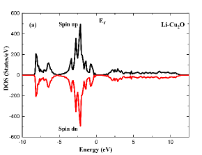
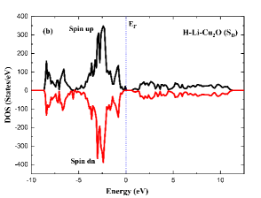
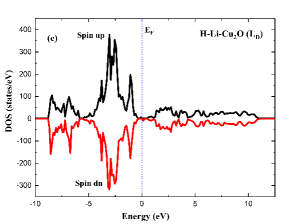
Figure 5 (a) shows the total densities of states for Li-doped Cu2O. From Fermi level position we note that the Li doped Cu2O is p-type characteristic. This result agrees well with the experimental work of Kyung-Su Cho et al. [50] where they used Li doped Cu2O as p-type in p-n heterojunction. The calculated band gap of Li-doped Cu2O is 0.61 eV.
From the DOS figures [figure 5 (b), figure 5 (c)] of H-Li-doped, we see the shift in the Fermi level position. The hydrogen implantation in Li-doped Cu2O does not change the value of the band gap but it makes the Cu2O an n-type semiconductor characteristic. The distance between Li and H does not influence the band gap value of Li-doped Cu2O.
3.4 Ti and H doped Cu2O
For the first configuration (S), the distance between Ti and H is 1.8 Å. After the relaxation, the distance becomes 1.88 Å. In the second case configuration (L), the distance between Ti and H was 7.92 Å. After the relaxation, the distance becomes 7.9 Å.
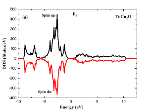
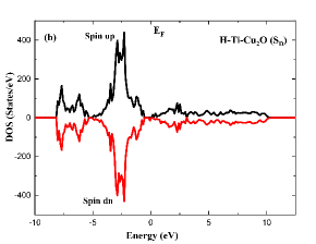
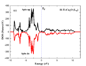
Figure 6 shows the total densities of states for Ti-doped Cu2O and H-Ti-doped Cu2O. The calculated band gap of Ti-doped Cu2O is 0.73 eV and 0.86 eV for the majority-spin and minority-spin electron, respectively. These values are larger than that of the pure Cu2O (0.55 eV). From the DOS figures, we note that Ti doping changes the position of Fermi level from near the valence band towards the conduction band, leading the system to n-type semiconductor characteristic. In the first case configuration, the hydrogen implantation can decrease the band gap value of Ti doped Cu2O to 0.59 eV, while in the second case configuration, hydrogen does not change the band gap value. In the two configurations, it does not change the conductivity type of Ti doped Cu2O.
| (eV) | (Å) | |
|---|---|---|
| Cu2O | 0.55 | 4.26 |
| H-Cu2O (spin up) | 0.46 | 4.28 |
| H-Cu2O (spin dn) | 0.23 | – |
| Na-Cu2O | 0.35 | 4.26 |
| H-Na-Cu2O (S) | 0.47 | 4.27 |
| H-Na-Cu2O (L) (spin up) | 0.47 | 4.27 |
| H-Na-Cu2O (L) (spin dn) | 0.35 | – |
| Li-Cu2O | 0.61 | 4.12 |
| H-Li-Cu2O (S) | 0.61 | 4.11 |
| H-Li-Cu2O (L) | 0.61 | 4.11 |
| Ti-Cu2O (spin up) | 0.73 | 4.11 |
| Ti-Cu2O (spin dn) | 0.86 | – |
| H-Ti-Cu2O (S) | 0.59 | 4.24 |
| H-Ti-Cu2O(L) | 0.86 | 4.12 |
Table 2 shows the calculated band energies () and lattice parameters (a) for Cu2O and M doped Cu2O with or without hydrogen. From this table, we can see that the band gap value of Na doping Cu2O makes it the best of the three as a p-type dopant in Cu2O. Compared with the value of pure Cu2O, the lattice parameter of Na doped Cu2O does not change while Li and Ti doping should compress the lattice of Cu2O. For all cases, hydrogen does not change the lattice of systems except with hydrogen implantation in the first configuration (S) in Ti doped Cu2O. In this configuration, hydrogen should expand the lattice of this system from 4.11 to 4.24 Å.
From the densities of states figures, we can see that hydrogen creates new states in the band gap in all systems. Na and Li act as acceptor impurities in Cu2O and hydrogen should passivate these acceptors. Ti is a source of n-type conductivity and hydrogen could not passivate this donor in Cu2O.
In the cases of H doped Cu2O, Ti doped Cu2O and H-Na-co-doped Cu2O for the second configuration (L), the diference in band gap value of majority-spin and minority-spin electrons shows anisotropy of the gap which determines the elastic distribution between the hole states and electrons.
From these results, it seems that hydrogen can passivate the acceptors (Na, Li) or donors (Ti) in Cu2O. Similar results have been found in experimental works; Lu et al. [51] revealed that a treatment of N-doped Cu2O films in hydrogen plasma could passivate the carrier traps. On the other hand, Ishizuka et al. [52, 53] show that a treatment of N-doped Cu2O films in hydrogen plasma leads to an increase of conductivity.
3.5 Magnetic and optical properties
We list the values of the total and local magnetic moments in table 3. With hydrogen, we have the values of the total magnetic moments approximately equal to 1 except with Ti-doped Cu2O, where it is almost zero. In all systems, the Cu moments dominate the values of local magnetic moments with a maximum value of 0.16 excluding the H-Ti-codoped Cu2O system where local magnetic moments values are negative.
| () | () | () | () | () | () | () | |
| Cu2O | 0.0 | – | – | – | – | 0.0 | 0.0 |
| H-Cu2O | 0.9999 | 0.056 | – | – | – | 0.13 | 0.05 |
| Na-Cu2O | 0.0 | – | 0.0 | – | – | 0.0 | 0.0 |
| H-Na-Cu2O (S) | 1.0 | 0.056 | 0.004 | – | – | 0.16 | 0.06 |
| H-Na-Cu2O (L) | 0.9999 | 0.058 | 0.0 | – | – | 0.12 | 0.05 |
| Li-Cu2O | 0.0 | – | – | 0.0 | – | 0.0 | 0.0 |
| H-Li-Cu2O (S) | 1.0 | 0.06 | – | 0.013 | – | 0.15 | 0.06 |
| H-Li-Cu2O (L) | 0.9955 | 0.06 | – | 0.0 | – | 0.12 | 0.04 |
| Ti-Cu2O | 1.0 | – | – | – | 0.75 | 0.024 | – 0.012 |
| H-Ti-Cu2O (S) | – 0.0006 | 0.0 | – | – | 0.05 | 0.02 | – 0.007 |
| H-Ti-Cu2O(L) | 0.0699 | – 0.07 | – | – | 0.74 | – 0.11 | – 0.05 |
As far as the principle of contamination of the samples by ferromagnetic impurities can be discounted, the common factor in all cases is crystal defects. Here, they have been established, but it is plausible that they are point defects-atomic vacancies or interstitials. Examples of ferromagnetism have been reported in the literature [54].
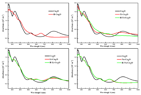
The absorption coefficient is important to estimate the optical properties of Cu2O and H-M-codoped Cu2O (M= Na, Li, Ti) used in photovoltaic cells or as optoelectronic devices. A material with a low absorption coefficient means more transmitted light. Cuprous oxide Cu2O is a promising p-type TCO, but its relatively low band gap (2.1 eV) limits its optical transmittance in the visible spectrum. In this paper, we aim at increasing this value.
Figure 7 presents the absorption coefficient (of the order of 104 cm-1) versus the wavelength (nm) of all configurations compared to the pure compound Cu2O in the visible light region (400–900 nm) and UV region (250–400 nm). The absorbance of pure Cu2O decreases from 1.92 cm-1 to 0.89 cm-1 in (250–400 nm) and in the visible region continues to decrease to 0.086 at 650 nm but we observed two peaks at 530 (0.287 cm-1) and 800 nm (0.428 cm-1). However, we noticed a small change when the M (Na, Li, Ti) atoms are at the cation sites (Cu) in the pure Cu2O. We remark the same peaks when we doped with Na with a small displacement of the second peak (from 800 to 650 nm). The Li or Ti doped Cu2O gives the same result in visible and UV regions but without the initial peak recorded in the pure system, and the absorbance increases between 650 and 750 nm. Furthermore, incorporation of Hydrogen reduces the absorbance of pure Cu2O and Ti doped Cu2O. Hydrogen does not decrease the absorbance of Na or Li-doped Cu2O.
4 Conclusion
We studied the electronic properties of M-doped Cu2O (M= Na, Li, Ti) with and without hydrogen by first-principles calculations. The results show that hydrogen is most stable in the tetrahedral site with the low formation energy. Interstitial hydrogen reduces the band gap value of Cu2O and it gives an n-type conduction behavior. Adding hydrogen does not decrease the band gap value of Na or Li-doped Cu2O but it changes the charges conductivity type from p- to n-type. In these cases, the distance between H atom and Na or Li atom does not affect the structural and electronic properties of Na or Li-doped Cu2O systems. The Ti doping of Cu2O changes its conductivity type. Hydrogen does not change the n-type characteristic of Ti doped Cu2O system (hydrogen effect is negligible compared to that of Ti) but it decreases the magnetic moments of this system. The distance between H and Ti atoms can influence the structural, electronic and magnetic properties of Ti doped Cu2O. From these results, we see that Na is the best p-type dopant in the Cu2O and it is necessary to remove hydrogen in this material to achieve an increased performance. The absorption shows that Cu2O is a promising optical material in the visible region. In this paper, we established the effects of H, Ti, Li or Na doping, which lead to a significant decrease of the absorption, i.e., increase the optical transmittance. The results of this work make it possible to adapt Cu2O to several technological applications and to different scientific fields. In the next stage of our research, we will study the dopants concentration effects and we hope to confirm our results by experimental investigations.
Acknowledgements
This work was funded under the Algerian General Directorate of Scientific Research and Technological Development (DGRSDT).
References
- [1] Olsen L.C., Bohara R.C., Urie M.W., Appl. Phys. Lett., 1979, 34, 47, doi:10.1063/1.90593.
- [2] Rakhshani A.E., Solid-State Electron., 1986, 29, 7, doi:10.1016/0038-1101(86)90191-7.
- [3] Toth R.S., Kilkson R., Trivich D., J. Appl. Phys., 1960, 31, 1117, doi:10.1063/1.1735756.
- [4] O’Keeffe M., Moore W.J., J. Chem. Phys., 1961, 35, 1324, doi:10.1063/1.1732045.
- [5] McKinzie H.L., O’Keeffe M., Phys. Lett. A, 1967, 24, 137, doi:10.1016/0375-9601(67)90728-1.
- [6] Sagadevan S., Nanosci. Nanotechnol., 2013, 3, 62–74, doi:10.5923/j.nn.20130303.06.
- [7] Kiliç Ç., Zunger A., Phys. Rev. B, 2003, 68, 075201, doi:10.1103/PhysRevB.68.075201.
-
[8]
Otte K., Lippold G., Hirsch D., Gebhardt R.K., Chassé T., Appl. Surf. Sci., 2001, 179, 203,
doi:10.1016/S0169-4332(01)00280-X. - [9] Kolkovsky Vl., Kolkovsky V., Bonde Nielsen K., Dobaczewski L., Karczewzki G., Nylandsted Larsen A., Phys. Rev. B, 2009, 80, 165205, doi:10.1103/PhysRevB.80.165205.
-
[10]
Bekisli F., Stavola M., Beall Fowler W., Boatner L., Spahr E., Lüpke G., Phys. Rev. B, 2011, 84, 035213,
doi:10.1103/PhysRevB.84.035213. - [11] Janotti A., Van de Walle C.G., Nat. Mater., 2007, 6, 44, doi:10.1038/nmat1795.
- [12] Bihler C., Gerstmann U., Hoeb M., Graf T., Gjukic M., Schimdt W.G., Stutzmann M., Brandt M.S., Phys. Rev. B, 2009, 80, 205205, doi:10.1103/PhysRevB.80.205205.
- [13] Van de Walle C.G., Phys. Rev. Lett., 2000, 85, 1012, doi:10.1103/PhysRevLett.85.1012.
-
[14]
Larabi A., Mebarki M., Sari A., Merad G., J. Magn. Magn. Mater., 2018, 446, 192–199,
doi:10.1016/j.jmmm.2017.09.029. - [15] Rak Z.S., Mahanti S.D., Mandal K.C., J. Electron. Mater., 2009, 38, 1539, doi:10.1007/s11664-009-0751-1.
-
[16]
Larabi A., Merad G., Abdellaoui I., Sari A., Solid State Commun., 2016, 239, 44–48,
doi:10.1016/j.ssc.2016.04.011. -
[17]
Varley J.B., Janotti A., Singh A.K., Van de Walle C.G., Phys. Rev. B, 2009, 79, 245206,
doi:10.1103/PhysRevB.79.245206. -
[18]
Filippone F., Mattioli G., Alippi P., Amore Bonapasta A., Phys. Rev. B, 2009, 80, 245203,
doi:10.1103/PhysRevB.80.245203. -
[19]
Cox S.F.J., Davis E.A., Cottrell S.P., King P.J.C., Lord J.S., Gil J.M., Alberto H.V., Vilão R.C., Piroto Duarte J., Ayres de Campos N., Weidinger A., Lichti R.L., Irvine S.J.C., Phys. Rev. Lett., 2001, 86, 2601,
doi:10.1103/PhysRevLett.86.2601. - [20] Hofmann D.M., Hofstaetter A., Leiter F., Zhou H., Henecker F., Meyer B.K., Orlinskii S.B., Schmidt J., Baranov P.G., Phys. Rev. Lett., 2002, 88, 045504, doi:10.1103/PhysRevLett.88.045504.
-
[21]
Shimomura K., Nishiyama K., Kadono R., Phys. Rev. Lett., 2002, 89, 255505,
doi:10.1103/PhysRevLett.89.255505. - [22] Peacock P.W., Robertson J., Appl. Phys. Lett., 2003, 83, 2025, doi:10.1063/1.1609245.
- [23] Scanlon D.O., Watson G.W., Phys. Rev. Lett., 2011, 106, 186403, doi:10.1103/PhysRevLett.106.186403.
- [24] Kresse G., Furthmüller J., Phys. Rev. B, 1996, 54, 11169, doi:10.1103/PhysRevB.54.11169.
- [25] Kresse G., Joubert D., Phys. Rev. B, 1999, 59, 1758, doi:10.1103/PhysRevB.59.1758.
- [26] Perdew J.P., Burke K., Ernzerhof M., Phys. Rev. Lett., 1969, 77, 3865, doi:10.1103/PhysRevLett.77.3865.
- [27] Blöchl P.E., Phys. Rev. B, 1994, 50, 17953, doi:10.1103/PhysRevB.50.17953.
- [28] Hallberg J., Hanson R.C., Phys. Status Solidi B, 1970, 42, 305–310, doi:10.1002/pssb.19700420131.
-
[29]
Manghnani M.H., Brower W.S., Parker H.S., Phys. Status Solidi A, 1974, 25, 69–76,
doi:10.1002/pssa.2210250103. - [30] Korzhavyi P.A., Johansson B., Literature Review on the Properties of Cuprous Oxide Cu2O and the Process of Copper Oxidation, No. SKB-TR–11-08, Swedish Nuclear Fuel and Waste Management Co., Stockholm, 2011.
- [31] Laskowski R., Blaha P., Schwarz K., Phys. Rev. B, 2003, 67, 075102, doi:10.1103/PhysRevB.67.075102.
-
[32]
Zheng C., Tao Y., Cao J.-Z, Chen R.-F., Zhao P., Wu X.-J., Huang W., J. Mol. Model., 2012, 18, 4929,
doi:10.1007/s00894-012-1483-3. - [33] Reshak A.H., Auluck S., Phys. Rev. B, 2003, 68, 125101, doi:10.1103/PhysRevB.68.125101.
- [34] Melrose D.B., Stoneham R.J., J. Phys. A: Math. Gen., 1977, 10, L17, doi:10.1088/0305-4470/10/1/004.
-
[35]
Van de Walle C.G., Denteneer P.J.H., Bar-Yam Y., Pantelides S.T.,
Phys. Rev. B, 1989, 39, 10791,
doi:10.1103/PhysRevB.39.10791. - [36] Neugebauer J., Van de Walle C.G., In: Hydrogen in Semiconductors II, Semiconductors and Semimetals, Vol. 61, Nickel N.H. (Ed.), Academic Press, Boston, 1999, 479–502.
- [37] Cox S.F.J., Lord J.S., Cottrell S.P., Gil J.M., Alberto H.V., Keren A., Prabhakaran D., Scheuermann R., Stoykov A., J. Phys.: Condens. Matter, 2006, 18, 1061, doi:10.1088/0953-8984/18/3/021.
- [38] McCluskey M.D., Tarun M.C., Teklemichael S.T., J. Mater. Res., 2012, 27, 2190, doi:10.1557/jmr.2012.137.
- [39] Mollwo E., Z. Angew. Phys., 1954, 138, 478, doi:10.1007/BF01340694.
- [40] Thomas D.G., Lander J.J., J. Chem. Phys., 1956, 25, 1136, doi:10.1063/1.1743165.
- [41] Lander J.J., J. Phys. Chem. Solids, 1957, 3, 87, doi:10.1016/0022-3697(57)90053-7.
- [42] Kittel C., Introduction to Solid State Physics, 6-th Ed., Wiley, New York, 1986.
- [43] Marksteiner P., Blaha P., Schwarz K., Z. Phys. B: Condens. Matter, 1986, 64, 119–127, doi:10.1007/BF01303692.
-
[44]
Martínez-Ruiz A., Moreno Ma.G., Takeuchi N., Solid State Sci., 2003, 5, 291–295,
doi:10.1016/S1293-2558(03)00003-7. - [45] Soon A., Todorova M., Delley B., Stampfl C., Phys. Rev. B, 2006, 73, 165424, doi:10.1103/PhysRevB.73.165424.
-
[46]
Islam M.M., Diawara B., Maurice V., Marcus P., J. Mol. Struct. THEOCHEM, 2009, 903, 41–48,
doi:10.1016/j.theochem.2009.02.037. -
[47]
Elfadill N.G., Hashim M.R., Chahrour K.M., Mohammed S.A., Semicond. Sci. Technol., 2016, 31, 065001,
doi:10.1088/0268-1242/31/6/065001. - [48] Minami T., Nishi Y., Miyata T., Appl. Phys. Express, 2015, 8, 022301, doi:10.7567/apex.8.022301.
- [49] Minami T., Yamazaki J., Miyata T., MRC Communcations, 2016, 6, 416–420, doi:10.1557/mrc.2016.45.
-
[50]
Cho K.-S., Kim D.-H., Kim Y.-H., Nah J.,
Kim H.-K., Ceram. Int., 2016, 43, 2279–2287,
doi:10.1016/j.ceramint.2016.10.208. - [51] Lu Y.-M., Chen C.-Y., Lin M.H., Thin Solid Films, 2005, 480–481, 482–485, doi:10.1016/j.tsf.2004.11.083.
- [52] Ishizuka S., Kato S., Okamoto Y., Akimoto K., Appl. Phys. Lett., 2002, 80, 950, doi:10.1063/1.1448398.
- [53] Ishizuka S., Kato S., Okamoto Y., Sakurai T., Akimoto K., Fujiwara N., Kobayashi H., Appl. Surf. Sci., 2003, 216, 94, doi:10.1016/S0169-4332(03)00485-9.
- [54] Coey J.M.D., Solid State Sci., 2005, 7, 660–667, doi:10.1016/j.solidstatesciences.2004.11.012.
Ukrainian \adddialect\l@ukrainian0 \l@ukrainian Ïåðøîïðèíöèïíå äîñëiäæåííÿ ïîâåäiíêè âîäíþ ó M-ëåãîâàíîìó Cu2O (M Na, Li i Ti) A. Ëÿðàái, A. Ìàõìóäi, M. Ìåáàðêi, M. Äåðãàë
Íàóêîâî-äîñëiäíèé öåíòð ç òåõíîëîãi¿ íàïiâïðîâiäíèêiâ äëÿ åíåðãåòèêè (CRTSE),
BP 140 Àëæèð 7- Ìåðâåé 16038, Àëæèð
Âiääiëåííÿ âèâчåííÿ òà ïðîãíîçóâàííÿ ìàòåðiàëiâ, âiääië äîñëiäæåíü ìàòåðiàëiâ òà âiäíîâëþâàíèõ äæåðåë åíåðãi¿, LEPM-URMER, Óíiâåðñèòåò Òëåìñåíà, Àëæèð