toltxlabel \zexternaldocument*[SI-]SI
Strain-induced stripe phase in charge ordered single layer NbSe2
Abstract
Charge density waves are ubiquitous phenomena in metallic transition metal dichalcogenides. In NbSe2, a triangular structural modulation is coupled to a charge modulation. Recent experiments reported evidence for a triangular-stripe transition at the surface, due to strain or accidental doping and associated to a modulation. We employ ab-initio calculations to investigate the strain-induced structural instabilities in a pristine single layer and analyse the energy hierarchy of the structural and charge modulations. Our results support the observation of phase separation between triangular and stripe phases in 1H-NbSe2, relating the stripe phase to compressive isotropic strain, favouring the modulation. The observed wavelength of the charge modulation is also reproduced with a good accuracy.
I Introduction
Transition metal dichalcogenides are among the most exciting hosts for ordered phases, such as superconductivity and charge/spin modulations Saito et al. (2016); Wilson et al. (1974, 2001); Moncton et al. (1975); Revolinsky et al. (1965) because of their cooperative interactions Kiss et al. (2007). In fact, their coexistence is counter-intuitive, being collective electronic modes which build an excitation gap, hence requiring a large number of electrons available at the Fermi level. Since early works Rice and Scott (1975); Liu et al. (1998); Straub et al. (1999), the transition to a charge/spin ordered state driven by the electron gas at the Fermi level has been questioned, partly because of the difficulties in explaining the intricate coexistence of superconductivity with charge density waves (CDWs) Wilson et al. (1974); Moncton et al. (1975); Revolinsky et al. (1965); Rahn et al. (2012); Castro Neto (2001); Cho et al. (2018). Among the proposed explanations, the electronically driven mechanism was ruled out Inosov et al. (2008); Rossnagel et al. (2001); Rossnagel and Smith (2007); Johannes et al. (2006); Johannes and Mazin (2008); Zhu et al. (2015); Ángel Silva-Guillén et al. (2016) in favor of a momentum-assisted mechanism Calandra et al. (2009); Valla et al. (2004); Rahn et al. (2012); Zheng et al. (2018); Arguello et al. (2014); Flicker and van Wezel (2015a); Zhu et al. (2015), which is likely influenced by external conditions, such as applied fields Galvis et al. (2018); Cho et al. (2018) or epitaxially induced strain Fu et al. (2017); Wei et al. (2017), and chemical Di Salvo et al. (1975); Chatterjee et al. (2015); Cossu et al. (2018) or gate Wei et al. (2017); Shao et al. (2016) doping.
Further intricacies in the occurrence of these collective electronic excitations arise at the surface and single layers due to a reduced symmetry. While the bulk, 2H type, is characterised by a symmetry, with centrosymmetry and inversion symmetry operations, the layer at the surface has no inversion symmetry and lacks a van der Waals bonded layer; its structural type remains 2H, although high reactivity to (accidental) dopants and diffusion into interstitial regions affect experimental investigations, modifying its structure and symmetry operations; the single layer is characterised by a symmetry, with an inversion symmetry operation but lack of centrosymmetry and no van der Waals bonded layers on either sides. In passing from the bulk to thin layers and down to a single layer, enhanced effects from fluctuations and lack of van der Waals bonded layers may determine dramatic changes in the structural and electronic degrees of freedom Kotov et al. (2012); Guinea et al. (2014); Mak et al. (2012); Frindt (1972); Xi et al. (2015); Ugeda et al. (2016); Butler et al. (2013); Geim and Grigorieva (2013); Novoselov et al. (2016); Ge and Liu (2012). Due to the fact that CDW consists of periodic lattice distortions coupled to charge modulations, structural properties may modify such collective excitation dramatically, and in turn its interplay with superconductivity Menard et al. (2015); Ugeda et al. (2016). In the case of 2H-NbSe2, the CDW is recognised to arise from a phonon instability Weber et al. (2011), inducing an electronic reconstruction in a sizable energy range Arguello et al. (2014) in the bulk and at the surface, although single layers show a CDW gap centred at the Fermi level Ugeda et al. (2016). Electronic and magnetic texture may be layer-resolved Riley et al. (2014); Bawden et al. (2016), contributing to a complex scenario to explain the thickness-dependent properties of these materials. Reduced dimensionality allows for different ways of tuning the crystal and the electronic structure. The competition between the trigonal prismatic (2H) and the octahedral (1T) phases becomes stronger; as a consequence, the 1T crystal phase, unstable in the bulk Kadijk and Jellinek (1971), may be synthesised Nakata et al. (2016) or induced by external sources Bischoff et al. (2017); the resulting charge order is not the usual star of David phase, unlike TaSe2 Liu et al. (2016); Börner et al. (2018) and TaS2 Law and Lee (2017); Fazekas and Tosatti (1980). In the 2H-type, Soumyanarayanan et al. (2013); Gao et al. (2018) and/or Gao et al. (2018) modulations, linked to a stripe phase at the surface, are reported. Distinct CDW structures, supporting the widely known CDW incommensurate character in 2H-NbSe2 Gye et al. (2019) are observed, further speculating on their topological connection. A change from the to the modulation was previously predicted by ab-initio studies on 2H/1H-type NbSe2 Calandra et al. (2009); Lian et al. (2018), but an early scanning tunnelling microscopy/spectroscopy (STM/STS) study Ugeda et al. (2016) confirms that the modulation dominates in single layers deposited on bilayer graphene; on the other hand, a recent theoretical study Flicker and van Wezel (2015b) showed that within a modulation, uniaxial strain leads to a triangular-stripe CDW transition in 2H-NbSe2. However, phase transitions remain often latent because they are suppressed by growth/synthesis conditions, choice of the substrate and/or quantum fluctuations. In this respect, discerning intrinsic from extrinsic characteristics is crucial to understand these phases and finding possible routes to their manipulation.
The present work focusses on 1H-NbSe2 single layers under isotropic biaxial strain. In order to shed light on the competition and coexistence of various periodicities and structures, we first perform phonon calculations, suggesting the wave-vectors of the structural instabilities. Thereafter, the suggested periodicities are investigated with a full set of total energy calculations, yielding both the energy hierarchy of the possible CDW structures and their charge distributions. A - (triangular-stripe) transition occurs in the modulation, whereas it is incipient in the modulation. Although our model represents only an approximation of detailed experimental conditions, e.g. due to the fact that we do not include a substrate, we believe it identifies the most important intrinsic characteristics of single layers under isotropic biaxial strain. Moreover, our results are likely applicable also to thin films, due to the fact that CDW properties depend on the structural properties more strongly than on the electronic properties, as well as due to the above mentioned high reactivity to accidental doping which may affect the structural features at the surface.
II Methods
| MM | MW | HX | CC | HC | CCccws | HXHC | HC | ||||
| = 3.49 | |||||||||||
| = 3.45 | |||||||||||
| = 3.41 | |||||||||||
Our results are obtained by ab initio calculations within the formalism of the density-functional theory (DFT). The projected augmented wave (PAW) method with Perdew-Burke-Ernzerhof (PBE) pseudopotentials Blöchl (1994); Kresse and Joubert (1999), as implemented in the Quantum ESPRESSO suite Giannozzi et al. (2009, 2017) and the Vienna Ab-initio Simulation Package (VASP), is used. The relaxation of the unit cell and the computation of its relative phononic spectra are run in the former code, while structural relaxation, total energy calculations and charge distributions are performed with the latter. The exchange-correlation functional is treated within the generalised gradient approximation using the PBE parametrisation Perdew et al. (1996, 1997). The pseudopotentials used in the simulations provide explicit treatment of the following valence electrons: for Nb and for Se. The cutoff energy of the plane waves for the unit cell (Quantum ESPRESSO) is and that for the supercell calculations is ; prior to the phonon calculations, an energy cutoff is also applied for the charge density and potential, of . The energy tolerance on the electronic loops for the calculations in the unit cell is , whereas it is for the calculations in the supercells ( for accurate determination of the electronic properties, such as density of electronic states and charge distributions). A conjugate gradient algorithm is employed for structural relaxation in all cases, with a tolerance in energy of per unit cell and a residual force of on each atom. The calculations of phonons are performed sampling the first Brillouin Zone with a k-grid (for the wavefunctions) and a q-grid (for the force constants). The formation of CDWs is analysed sampling the first Brillouin Zone by means of the , , , and grids of -points for the , , , and supercells, respectively, keeping approximately an equal distance between -points.
Finally, we also computed some quantities offering a more direct comparison to experimental data. Band structures were calculated using method of Popescu and Zunger Popescu and Zunger (2012). STM simulations were also performed, by means of the BSKAN code Hofer (2003); Palotás and Hofer (2005). The revised Chen method Mándi and Palotás (2015) with an electronically flat and spatially spherical tip orbital has been used, which is equivalent to the Tersoff-Hamann model of electron tunnelling Tersoff and Hamann (1985). The reported STM images are in constant current mode (with the maxima of the current contours at 5.8 Åfor all structures for a better comparability). Additional technical details on band structures and STM spectra are provided in the Appendix.
III Results and discussion
Structural relaxation of the unit cell was performed for three values of the lattice constant, , and , which aim at modelling the system under compressive strain (), no strain and tensile strain (), respectively. The precise value of the computed in-plane stress is , and , respectively. The small residual compressive strain present in the no-strain case is due to the choice of a standard literature value for the equilibrium lattice constant of the bulk, in line with the work of Fang et al. Fang et al. (2018). Since the discrepancy is very small, this detail does not affect the conclusions of the present work. A recent ab-initio study Ángel Silva-Guillén et al. (2016) reports a lattice constant of , in agreement with the residual strain found for in our calculations. The relaxed structures were used to compute phonon spectra, whose imaginary values identify regions of structural instability, thus speculating on the periodicity of the supercells describing the stable crystal. These supercells are then investigated by total energy calculations to confirm (or dismiss) the relevance of a periodicity and to evaluate the energy hierarchy of a set of symmetries within each periodicity. The lattice reconstructions considered on the basis of the analysis of phonon spectra are of the type Kamil et al. (2018) and (suggested by discussion of results from STM Gye et al. (2019)).
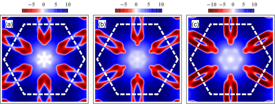
The phonon dispersions are represented as two-dimensional plots, Fig. 1, with positive (negative) values of ) shown in blue (red). Compressive strain, equilibrium, and tensile strain are shown from left to right, (a) to (c). The deepest troughs of the single layer phonon dispersion appear off the M line, as a consequence of the non-centrosymmetric character of the single layer (1H). The instabilities have to be interpreted as perturbations which drive the system away from its most symmetric configuration, providing only an indication, rather than a determination, of the resulting periodicities. A modulation is expected from the lowest values of the phonon dispersion, see especially Fig. 1 (b), where the troughs appear in couples at symmetric positions with respect to the M high symmetry line. Each couple of instability represent two periodic lattice distortions with opposite chirality. This result supports early Komori et al. (1997) and recent Wang et al. (2009) STM observations. In particular, a 2H-1T structural phase separation is reported in refs. Wang et al., 2009 and Bischoff et al., 2017; Nakata et al., 2016. Further, we note similarities between the phonon dispersion in the 1H-type and that in the 1T-type Kamil et al. (2018). Nevertheless, these instabilities may couple to give rise to a modulation, which is the most observed. In a similar fashion, instability regions around M may couple to give rise to a (or even a ) modulation. Instabilities are expected to dominate along M in a 2H-type symmetry (because the crystal is overall centrosymmetric).
Compressive strain reduces the instabilities along the MK line and the minima of dominate around 2/4 M (off the high symmetry line), see Fig. 1 (a), pointing towards a modulation. Conversely, a zone of instability centered around, but not including, M becomes dominant under tensile strain, pointing towards a modulation; further local minima of appear at 2/4 M, Fig. 1 (c), justifying recent reports Gao et al. (2018) for which both and periodicities arise under tensile strain.
After having found the most likely periodicities for the occurrence of periodic lattice distortions by the calculation of phonon spectra, we investigate a set of structures for each periodicity by total energy calculation; in particular, the distorted structures we start with have fewer point symmetry operations with respect to the full symmetric structure, and model a periodic lattice distortion with three-fold rotational symmetry. In order to keep a close connection to existing materials, we also explore periodicities compatible with experimental findings Gao et al. (2018); Gye et al. (2019). We study a representative number of structures for each periodicity (in the periodicity we study three known CDW structures Cossu et al. (2018); Gye et al. (2019); Malliakas and Kanatzidis (2013); Lian et al. (2018) anew, complementing previous works by showing the energy hierarchy upon strain); here we refer to them as hexagonal (HX), chalcogen centered triangular (CC) and hollow centered triangular (HC). Energy differences, shown in Table 1, are used to test whether and how each periodicity can give rise to a CDW structure.
All structures tested in our calculations relaxed to the symmetric structure, for all values of the strain; therefore, the periodicity in ref. Gao et al., 2018 does not arise from an intrinsic character of a single layer. The periodicity accounts for the occurrence of instabilities at 2/3 M and at M; compare with ref. Gye et al., 2019, figure 3, where HC and CC merge. The energy hierarchy between CDW structures with periodicity is in agreement with existing ab-initio studies Lian et al. (2018); Cossu et al. (2018). The and the periodicities allow the relaxation of three structures each, energetically close to the known CDWs. In particular, the CDW structures are favoured over the CDW ground state under compressive strain. In general, a plethora of structural modulations are available in single layer NbSe2, whose competition depends and may be tuned by epitaxial strain, charge transfer or proximity effects.
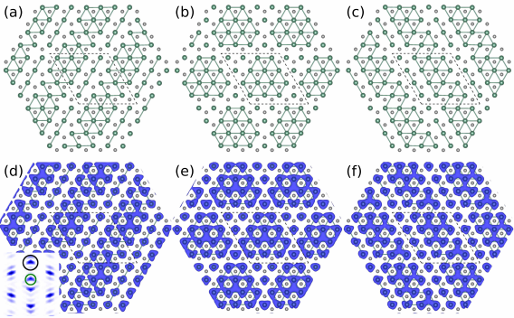
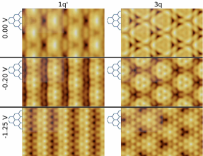
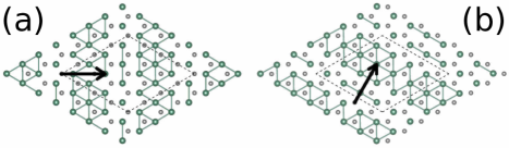
All starting structures for all the supercells considered here have been given a symmetry compatible with a triple ordering vector for the lattice distortion. The relaxed structures are found in accordance; however, we find a surprising result in one supercell. A total of three relaxed structures are identified within the periodicity; two of them are characterised by a single ordering vector and referred to as and (Figs. 2 (a) and (c), respectively); a third one, referred to as , is characterised by three equivalent ordering vectors, see Fig. 2 (b); it is energetically unfavoured at the equilibrium lattice constant and degenerates into the () for compressive (tensile) strain. The wavelength of the and the charge distributions is (, where is the lattice constant of the unstrained unit cell), () and (), for compressive strain, no strain and tensile strain respectively, for both phases. These results show a strong connection between the phases shown in Fig. 2 and the stripe phase observed at the surface Soumyanarayanan et al. (2013); Gao et al. (2018). In fact, two features of the modelled CDWs are shown to be in remarkable agreement with experiments: the Fourier transform of the charge distribution – compare the inset of Fig. 2 with that resulting from STM in figure 1F in ref. Gao et al., 2018 – and the wavelength of the modulation – compare our result with the measured wavelength from STM data, Soumyanarayanan et al. (2013), . Further comparison to these experimental features is provided by our simulated STM plots of the phase, shown in Fig. 3, left column. Additional STM plots, as well as a more extensive discussion, are reported in the Appendix.
The previous analysis of the stripe phase is based on the comparison between our calculations for the single layer (1H) and experimental results for the surface (2H). As pointed out in the Introduction, these systems have different characteristics and therefore a certain care is needed when comparing them. To support our conclusions, we also performed selected calculations for the bilayer, whose symmetries and physical properties are a better model of the surface. Relevant structures with and periodicities were simulated, and the latter were found to be more favourable of with respect to the former (compare with Table 1). Further details on these calculations are presented in the Appendix. Finally, it is also important to comment on the fact that the stripe phase remains unobserved in single layers (1H), see e.g. ref. Ugeda et al., 2016. This is likely due to unfavourable or insufficient epitaxial strain of the substrates where the single layers are deposited, whereas applied Gao et al. (2018) and/or accidental strain Soumyanarayanan et al. (2013) favour such transition. A recent paper by Kim et al. Kim and Son (2017) discussed this point in terms of dielectric screening (comparing two different substrates), elucidating the role of spin-orbit coupling in the electronic properties and in the CDW formation.
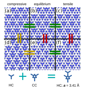
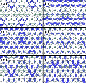
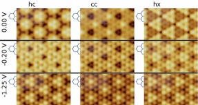
The emergence of a stripe phase under isotropic simulated strain reveals an intrinsic tendency for the CDW towards a lower symmetry, which manifests in the periodicity and remains latent in the periodicity. In a recent paper Flicker and van Wezel (2015b), calculations based on a Ginzburg-Landau formalism show that phonon fluctuations suppress long-range order in favour of a short-ranged pseudogap phase with a phase, which degenerates into a phase upon uniaxial strain. The authors restrained their study to a CDW. Within superlattices, with (biaxial) isotropic strain, we cannot find a stripe phase either, and even when a stripe structure is given as an input, it degenerates into a triangular CDW (CC or HC, depending on the starting input). All in all, isotropic strain induces only an incipient stripe phase with a periodicity, see Fig. 4. The HC and CC CDW patches are distinct under tensile strain (c,f) and at the equilibrium lattice constant (b,e), compare the three-spikes ring in the CC CDW with the three-fold fidget-spinner-like star in the HC CDW, but the HC degenerates into the CC for compressive strain (a,d), where the rings and stars patches are merged.
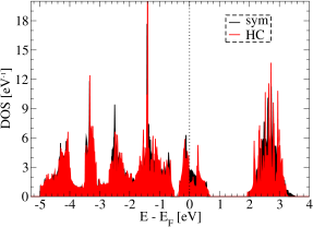
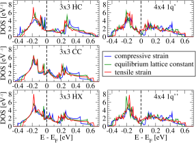
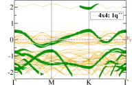
On the other hand, allowing the periodicity, in agreement with the imaginary phonon dispersion, enhances the degrees of freedom and widens the ordering parameters space. Such periodicity hosts both single and triple phases, and therefore is suitable to analyse a relation between the electronic reconstruction and the symmetry of the ordering vectors. We consider the electron-phonon coupling as the driving mechanism for the CDW, as widely reported in the literature. In a Peierls instability scenario, where the electrons dominate over the phonons in driving the transition, a CDW results in a spectral weight loss at the Fermi level, which is also consistent with a weak-coupling. It has been already shown Johannes et al. (2006); Ángel Silva-Guillén et al. (2016) that it is not the case of NbSe2, where instead the electronic spectral weight shifts are more important at a lower energy range, implying that the transition is governed by phonons (note also the presence of electronic states below the Nb-derived band and its dependence on the CDW, in ref. Ángel Silva-Guillén et al., 2016). Figure 5 shows the density of the electronic states (DOS) of the single-vector CDWs (denoted both as because their DOS curves have no substantial difference), the CDW structure and the undistorted structure. A steep curve, showing increase (depletion) of states below (above) the Fermi level, characterises the CDW, whereas the CDW features a depletion of spectral weight all around the Fermi level. The CDW displays also a clear and narrow dip at . A more detailed analyis of the spectral properties, complemented with unfolded band structures, is reported in the Appendix.
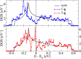
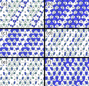
Charge density distributions of the and CDWs in direct space are reported in Figs. 6 and 7, respectively. These data show a phase change of the electronic modulation across , in analogy with ref. Arguello et al., 2014. Starting from the Fermi level, see Fig. 6 (e), the CDW has a symmetry which is maintained down to , see Fig. 6 (c); below this energy, the symmetry is reduced to a single . On the other hand, the CDW survives down to , see Fig. 7, pointing to an even stronger phononic involvement in the transition for this phase. The lattice distortions induce variations of the DOS at several energy levels, see Fig. LABEL:SI-totdos-fig in the Appendix, with reference to the CDW ground state, and compare it with ref. Ángel Silva-Guillén et al., 2016; around and large variations occur. Note that the symmetry of the charge distribution has particular features depending on the energy range of the electrons. As CDW-induced spectral weight shifts may differ in intensity at different energy ranges, STS maps may differ from STM maps; for example, Fig. 3 shows that the phase still exhibits a three-fold symmetry for all indicated bias voltages in constant-current STM images, where the electronic states are integrated within a corresponding energy window (from the Fermi level to the bias voltage).
IV Conclusions
In conclusion, we analysed the lattice distortions and their accompanying charge modulations in single layer 1H-NbSe2 under biaxial isotropic strain, finding that a compressive strain
of favours modulations with a single ordering vector. Together with two phases characterised by a single ordering vector, a metastable triple ordering
vector phase exists. On the other hand, modulations allow only an incipient - transition under strain, but the charge patches of the ground state CDW
structure assume features from the next most favourable structure. Although the strain in our model may not have been applicable by suitable (e.g. chemically non-reactive) substrates so
far, the present study offers insights on the intrinsic properties of the single layer NbSe2, which can be useful for future experimental investigations on the manipulation of collective
excitations in NbSe2 and related transition metal dichalcogenides. Moreover, we observe that the stripe phase observed in NbSe2 thin films is very likely associated to
modulations, and favoured by compressive strain.
V Acknowledgements
We are grateful to Yunkyu Bang, Poonam Kumari, Dhani Milind Nafday, Erio Tosatti, Stefano de Gironcoli, Ali G. Moghaddam, Tristan Cren,
Hermann Suderow and Han-Woong Yeom for insightful discussions. F. C. and A. A. acknowledge financial support from the National Research
Foundation (NRF) funded by the Ministry of Science of Korea (Grants No. 2016K1A4A01922028, No. 2017R1D1A1B03033465, & No. 2019R1H1A2039733); K. P. acknowledges support from NRDIO-Hungary project No. FK124100. This research was supported by appointments to the JRG program at the APCTP
through the Science and Technology Promotion Fund and Lottery Fund of the Korean Government, and by the Korean Local Governments –
Gyeongsangbuk-do province and Pohang City.
References
- Saito et al. (2016) Y. Saito, T. Nojima, and Y. Iwasa, Nature Reviews Materials 2, 16094 (2016).
- Wilson et al. (1974) J. A. Wilson, F. J. Di Salvo, and S. Mahajan, Phys. Rev. Lett. 32, 882 (1974).
- Wilson et al. (2001) J. A. Wilson, F. J. D. Salvo, and S. Mahajan, Adv. Phys. 50, 1171 (2001).
- Moncton et al. (1975) D. E. Moncton, J. D. Axe, and F. J. DiSalvo, Phys. Rev. Lett. 34, 734 (1975).
- Revolinsky et al. (1965) E. Revolinsky, G. A. Spiering, and B. D. J., J. Phys. Chem. Solids 26, 1029 (1965).
- Kiss et al. (2007) T. Kiss, T. Yokoya, A. Chainani, S. Shin, T. Hanaguri, M. Nohara, and H. Takagi, Nat. Phys. 3, 720 (2007).
- Rice and Scott (1975) T. M. Rice and G. K. Scott, Phys. Rev. Lett. 35, 120 (1975).
- Liu et al. (1998) R. Liu, C. G. Olson, W. C. Tonjes, and R. F. Frindt, Phys. Rev. Lett. 80, 5762 (1998).
- Straub et al. (1999) T. Straub, T. Finteis, R. Claessen, P. Steiner, S. Hüfner, P. Blaha, C. S. Oglesby, and E. Bucher, Phys. Rev. Lett. 82, 4504 (1999).
- Rahn et al. (2012) D. J. Rahn, S. Hellmann, M. Kalläne, C. Sohrt, T. K. Kim, L. Kipp, and K. Rossnagel, Phys. Rev. B 85, 224532 (2012).
- Castro Neto (2001) A. H. Castro Neto, Phys. Rev. Lett. 86, 4382 (2001).
- Cho et al. (2018) K. Cho, M. Konczykowski, S. Teknowijoyo, M. A. Tanatar, J. Guss, P. B. Gartin, J. M. Wilde, A. Kreyssig, R. J. McQueeney, A. I. Goldman, V. Mishra, P. J. Hirschfeld, and R. Prozorov, Nat. Commun. 9, 2796 (2018).
- Inosov et al. (2008) D. S. Inosov, V. B. Zabolotnyy, D. V. Evtushinsky, A. A. Kordyuk, B. Büchner, R. Follath, H. Berger, and S. V. Borisenko, New J. Phys. 10, 125027 (2008).
- Rossnagel et al. (2001) K. Rossnagel, O. Seifarth, L. Kipp, M. Skibowski, D. Voß, P. Krüger, A. Mazur, and J. Pollmann, Phys. Rev. B 64, 235119 (2001).
- Rossnagel and Smith (2007) K. Rossnagel and N. V. Smith, Phys. Rev. B 76, 073102 (2007).
- Johannes et al. (2006) M. D. Johannes, I. I. Mazin, and C. A. Howells, Phys. Rev. B 73, 205102 (2006).
- Johannes and Mazin (2008) M. D. Johannes and I. I. Mazin, Phys. Rev. B 77, 165135 (2008).
- Zhu et al. (2015) X. Zhu, Y. Cao, J. Zhang, E. W. Plummer, and J. Guo, Proc. Natl. Acad. Sci. 112, 2367 (2015).
- Ángel Silva-Guillén et al. (2016) J. Ángel Silva-Guillén, P. Ordejón, F. Guinea, and E. Canadell, 2D Materials 3, 035028 (2016).
- Calandra et al. (2009) M. Calandra, I. I. Mazin, and F. Mauri, Phys. Rev. B 80, 241108 (2009).
- Valla et al. (2004) T. Valla, A. V. Fedorov, P. D. Johnson, P.-A. Glans, C. McGuinness, K. E. Smith, E. Y. Andrei, and H. Berger, Phys. Rev. Lett. 92, 086401 (2004).
- Zheng et al. (2018) F. Zheng, Z. Zhou, X. Liu, and J. Feng, Phys. Rev. B 97, 081101 (2018).
- Arguello et al. (2014) C. J. Arguello, S. P. Chockalingam, E. P. Rosenthal, L. Zhao, C. Gutiérrez, J. H. Kang, W. C. Chung, R. M. Fernandes, S. Jia, A. J. Millis, R. J. Cava, and A. N. Pasupathy, Phys. Rev. B 89, 235115 (2014).
- Flicker and van Wezel (2015a) F. Flicker and J. van Wezel, Nat. Commun. 6, 7034 (2015a).
- Galvis et al. (2018) J. A. Galvis, E. Herrera, C. Berthod, S. Vieira, I. Guillamón, and H. Suderow, Commun. Phys. 1, 30 (2018).
- Fu et al. (2017) Z.-G. Fu, J.-H. Wang, Y. Yang, W. Yang, L.-L. Liu, Z.-Y. Hu, and P. Zhang, EPL (Europhysics Letters) 120, 17006 (2017).
- Wei et al. (2017) M. J. Wei, W. J. Lu, R. C. Xiao, H. Y. Lv, P. Tong, W. H. Song, and Y. P. Sun, Phys. Rev. B 96, 165404 (2017).
- Di Salvo et al. (1975) F. J. Di Salvo, J. A. Wilson, B. G. Bagley, and J. V. Waszczak, Phys. Rev. B 12, 2220 (1975).
- Chatterjee et al. (2015) U. Chatterjee, J. Zhao, M. Iavarone, R. Di Capua, J. P. Castellan, G. Karapetrov, C. D. Malliakas, M. G. Kanatzidis, H. Claus, J. P. C. Ruff, F. Weber, J. van Wezel, J. C. Campuzano, R. Osborn, M. Randeria, N. Trivedi, M. R. Norman, and S. Rosenkranz, Nat. Commun. 6, 6313 (2015).
- Cossu et al. (2018) F. Cossu, A. G. Moghaddam, K. Kim, H. A. Tahini, I. Di Marco, H.-W. Yeom, and A. Akbari, Phys. Rev. B 98, 195419 (2018).
- Shao et al. (2016) D. F. Shao, R. C. Xiao, W. J. Lu, H. Y. Lv, J. Y. Li, X. B. Zhu, and Y. P. Sun, Phys. Rev. B 94, 125126 (2016).
- Kotov et al. (2012) V. N. Kotov, B. Uchoa, V. M. Pereira, F. Guinea, and A. H. Castro Neto, Rev. Mod. Phys. 84, 1067 (2012).
- Guinea et al. (2014) F. Guinea, M. I. Katsnelson, and T. O. Wehling, Ann. Phys. 526, A81 (2014).
- Mak et al. (2012) K. F. Mak, K. He, C. Lee, G. H. Lee, J. Hone, T. F. Heinz, and J. Shan, Nat. Mater. 12, 207 (2012).
- Frindt (1972) R. F. Frindt, Phys. Rev. Lett. 28, 299 (1972).
- Xi et al. (2015) X. Xi, L. Zhao, Z. Wang, H. Berger, L. Forró, J. Shan, and K. F. Mak, Nat Nano 10, 765 (2015).
- Ugeda et al. (2016) M. M. Ugeda, A. J. Bradley, Y. Zhang, S. Onishi, Y. Chen, W. Ruan, C. Ojeda-Aristizabal, H. Ryu, M. T. Edmonds, H.-Z. Tsai, A. Riss, S.-K. Mo, D. Lee, A. Zettl, Z. Hussain, Z.-X. Shen, and M. F. Crommie, Nat. Phys. 12, 92 (2016).
- Butler et al. (2013) S. Z. Butler, S. M. Hollen, L. Cao, Y. Cui, J. A. Gupta, H. R. Gutiérrez, T. F. Heinz, S. S. Hong, J. Huang, A. F. Ismach, E. Johnston-Halperin, M. Kuno, V. V. Plashnitsa, R. D. Robinson, R. S. Ruoff, S. Salahuddin, J. Shan, L. Shi, M. G. Spencer, M. Terrones, W. Windl, and J. E. Goldberger, ACS Nano 7, 2898 (2013).
- Geim and Grigorieva (2013) A. K. Geim and I. V. Grigorieva, Nature 499, 419 (2013).
- Novoselov et al. (2016) K. S. Novoselov, A. Mishchenko, A. Carvalho, and A. H. Castro Neto, Science 353, aac9439 (2016).
- Ge and Liu (2012) Y. Ge and A. Y. Liu, Phys. Rev. B 86, 104101 (2012).
- Menard et al. (2015) G. C. Menard, S. Guissart, C. Brun, S. Pons, V. S. Stolyarov, F. Debontridder, M. V. Leclerc, E. Janod, L. Cario, D. Roditchev, P. Simon, and T. Cren, Nat. Phys. 11, 1013 (2015).
- Weber et al. (2011) F. Weber, S. Rosenkranz, J.-P. Castellan, R. Osborn, R. Hott, R. Heid, K.-P. Bohnen, T. Egami, A. H. Said, and D. Reznik, Phys. Rev. Lett. 107, 107403 (2011).
- Riley et al. (2014) J. M. Riley, F. Mazzola, M. Dendzik, M. Michiardi, T. Takayama, L. Bawden, C. Granerød, M. Leandersson, T. Balasubramanian, M. Hoesch, T. K. Kim, H. Takagi, W. Meevasana, P. Hofmann, M. . S. Bahramy, J. . W. Wells, and P. . D. C. King, Nat. Phys. 10, 835 (2014).
- Bawden et al. (2016) L. Bawden, S. P. Cooil, F. Mazzola, J. M. Riley, L. J. Collins-McIntyre, V. Sunko, K. W. B. Hunvik, M. Leandersson, C. M. Polley, T. Balasubramanian, T. K. Kim, M. Hoesch, J. W. Wells, G. Balakrishnan, M. S. Bahramy, and P. D. C. King, Nat. Commun. 7, 11711 (2016).
- Kadijk and Jellinek (1971) F. Kadijk and F. Jellinek, Journal of the Less Common Metals 23, 437 (1971).
- Nakata et al. (2016) Y. Nakata, K. Sugawara, R. Shimizu, Y. Okada, P. Han, T. Hitosugi, K. Ueno, T. Sato, and T. Takahashi, NPG Asia Materials 8, e321 (2016).
- Bischoff et al. (2017) F. Bischoff, W. Auwärter, J. V. Barth, A. Schiffrin, M. Fuhrer, and B. Weber, Chem. Mater. 29, 9907 (2017).
- Liu et al. (2016) Y. Liu, D. F. Shao, L. J. Li, W. J. Lu, X. D. Zhu, P. Tong, R. C. Xiao, L. S. Ling, C. Y. Xi, L. Pi, H. F. Tian, H. X. Yang, J. Q. Li, W. H. Song, X. B. Zhu, and Y. P. Sun, Phys. Rev. B 94, 045131 (2016).
- Börner et al. (2018) P. C. Börner, M. K. Kinyanjui, T. Björkman, T. Lehnert, A. V. Krasheninnikov, and U. Kaiser, Appl. Phys. Lett. 113, 173103 (2018).
- Law and Lee (2017) K. T. Law and P. A. Lee, Proc. Natl. Acad. Sci. 114, 6996 (2017).
- Fazekas and Tosatti (1980) P. Fazekas and E. Tosatti, Physica B+C 99, 183 (1980).
- Soumyanarayanan et al. (2013) A. Soumyanarayanan, M. M. Yee, Y. He, J. van Wezel, D. J. Rahn, K. Rossnagel, E. W. Hudson, M. R. Norman, and J. E. Hoffman, Proc. Natl. Acad. Sci. 110, 1623 (2013).
- Gao et al. (2018) S. Gao, F. Flicker, R. Sankar, H. Zhao, Z. Ren, B. Rachmilowitz, S. Balachandar, F. Chou, K. S. Burch, Z. Wang, J. van Wezel, and I. Zeljkovic, Proc. Natl. Acad. Sci. 115, 6986 (2018).
- Gye et al. (2019) G. Gye, E. Oh, and H. W. Yeom, Phys. Rev. Lett. 122, 016403 (2019).
- Lian et al. (2018) C.-S. Lian, C. Si, and W. Duan, Nano Letters 18, 2924 (2018).
- Flicker and van Wezel (2015b) F. Flicker and J. van Wezel, Phys. Rev. B 92, 201103 (2015b).
- Blöchl (1994) P. E. Blöchl, Phys. Rev. B 50, 17953 (1994).
- Kresse and Joubert (1999) G. Kresse and D. Joubert, Phys. Rev. B 59, 1758 (1999).
- Giannozzi et al. (2009) P. Giannozzi, S. Baroni, N. Bonini, M. Calandra, R. Car, C. Cavazzoni, D. Ceresoli, G. L. Chiarotti, M. Cococcioni, I. Dabo, A. D. Corso, S. de Gironcoli, S. Fabris, G. Fratesi, R. Gebauer, U. Gerstmann, C. Gougoussis, A. Kokalj, M. Lazzeri, L. Martin-Samos, N. Marzari, F. Mauri, R. Mazzarello, S. Paolini, A. Pasquarello, L. Paulatto, C. Sbraccia, S. Scandolo, G. Sclauzero, A. P. Seitsonen, A. Smogunov, P. Umari, and R. M. Wentzcovitch, J. Phys.: Condens. Matter 21, 395502 (2009).
- Giannozzi et al. (2017) P. Giannozzi, O. Andreussi, T. Brumme, O. Bunau, M. B. Nardelli, M. Calandra, R. Car, C. Cavazzoni, D. Ceresoli, M. Cococcioni, N. Colonna, I. Carnimeo, A. D. Corso, S. de Gironcoli, P. Delugas, R. A. DiStasio, A. Ferretti, A. Floris, G. Fratesi, G. Fugallo, R. Gebauer, U. Gerstmann, F. Giustino, T. Gorni, J. Jia, M. Kawamura, H.-Y. Ko, A. Kokalj, E. Küçükbenli, M. Lazzeri, M. Marsili, N. Marzari, F. Mauri, N. L. Nguyen, H.-V. Nguyen, A. O. de-la Roza, L. Paulatto, S. Poncé, D. Rocca, R. Sabatini, B. Santra, M. Schlipf, A. P. Seitsonen, A. Smogunov, I. Timrov, T. Thonhauser, P. Umari, N. Vast, X. Wu, and S. Baroni, J. Phys.: Condens. Matter 29, 465901 (2017).
- Perdew et al. (1996) J. P. Perdew, K. Burke, and M. Ernzerhof, Phys. Rev. Lett. 77, 3865 (1996).
- Perdew et al. (1997) J. P. Perdew, K. Burke, and M. Ernzerhof, Phys. Rev. Lett. 78, 1396 (1997).
- Popescu and Zunger (2012) V. Popescu and A. Zunger, Phys. Rev. B 85, 085201 (2012).
- Hofer (2003) W. Hofer, Prog. Surf. Sci. 71, 147 (2003).
- Palotás and Hofer (2005) K. Palotás and W. A. Hofer, J. Phys.: Condens. Matter 17, 2705 (2005).
- Mándi and Palotás (2015) G. Mándi and K. Palotás, Phys. Rev. B 91, 165406 (2015).
- Tersoff and Hamann (1985) J. Tersoff and D. R. Hamann, Phys. Rev. B 31, 805 (1985).
- Fang et al. (2018) A. Fang, C. Adamo, S. Jia, R. J. Cava, S.-C. Wu, C. Felser, and A. Kapitulnik, Sci. Adv. 4, eaaq0330 (2018).
- Kamil et al. (2018) E. Kamil, J. Berges, G. Schönhoff, M. Rösner, M. Schüler, G. Sangiovanni, and T. O. Wehling, J. Phys.: Condens. Matter 30, 325601 (2018).
- Komori et al. (1997) F. Komori, T. Iwaki, K. Hattori, O. Shiino, and T. Hasegawa, J. Phys. Soc. Jpn. 66, 298 (1997), https://doi.org/10.1143/JPSJ.66.298 .
- Wang et al. (2009) H. Wang, J. Lee, M. Dreyer, and B. I. Barker, J. Phys.: Condens. Matter 21, 265005 (2009).
- Malliakas and Kanatzidis (2013) C. D. Malliakas and M. G. Kanatzidis, J. Am. Chem. Soc. 135, 1719 (2013).
- Kim and Son (2017) S. Kim and Y.-W. Son, Phys. Rev. B 96, 155439 (2017).
Supplemental material for
Triangular-stripe transition in charge ordered single layer NbSe2
by
Fabrizio Cossu, Krisztián Palotás, Sagar Sarkar, Igor Di Marco, and Alireza Akbari
VI Extended DOS and Phase shifts
In the main text, we presented the results for integrated charge density outside the energy range shown in Fig. 5 (main text). For completeness, we report the DOS of the HC CDW and the undistorted structure over an extended energy range in Fig. S1. This plot provides evidence for the presence of electronic states at various ranges and for the regions where major CDW-driven changes occur. We also analyse the phase shifts from Fig. 6 (main text) in more details. As discussed in the main text, the symmetry of this CDW is a around the Fermi level, and down to . Within the Nb-derived band, although maintaining a triple ordering vector, a inversion – Fig. 6 (c)-(d) (main text) – and a rigid shift of the charge patches – Fig. 6 (e)-(f) (main text) – occur; compare this trend with recent measurements SI-arguello-PRB.89.235115 . Conversely, the phases keep the same symmetry, see Fig. 7 (a)-(f) (main text). In the next section, we illustrate the STM maps at different tunnelling voltages. Furthermore, we compare the behaviour of the CDW in the superlattice with the CDWs in the superlattice. Further consideration is deserved by the strain-induced variations in the DOS, illustrated in Fig. S2. Important changes at the Fermi level are seen especially in the CDWs, where tensile (compressive) strain tends to increase (decrease) the spectral weight.
VII STM/STS
Simulations of STM were carried out by employing the BSKAN code SI-hofer-PSS2003 ; SI-palotas-JPCM2005 . The revised Chen method SI-mandi-PRB.91.165406 with an electronically flat and spatially spherical tip orbital is used, which is equivalent to the Tersoff-Hamann model of electron tunnelling SI-tersoff-PRB.31.805 . The reported STM images are in constant current mode (with the maxima of the current contours at 5.8 Angstroms for all structures for a better comparability).
The STM maps of the and CDWs are shown in Figs. S3 and 3 (main text), respectively. For the CDWs, we find a good agreement with existing experimental STM data SI-soumyanarayanan-PNAS2013 ; SI-ugeda-nphys2016 ; SI-arguello-PRB.89.235115 ; SI-chatterjee-ncomm2015 ; SI-gye_gc-PRL.122.016403 ; SI-gao-PNAS2018 ; SI-nakata-NPJ2DMA2018 . First, we point out that it is well known that the tip-sample distance can have a major influence on the observed STM contrasts, and a complete contrast reversal is also possible, see e.g. ref. SI-palotas-PRB.86.235415, . This effect is crucial for CDWs in hetero-layered structures such as transition metal dichalcogenides as well, where the more charged regions can be imaged as protrusions or depressions depending on the tip and tunneling conditions. In our case, modulations can result from a superposition of contribution from the transition metal layer and the chalcogen layer. As illustrated in figures 9 and 1 of ref. SI-cossu-PRB.98.195419 , the Se-Se bond patterns of CC and HX have the same symmetry as the Nb-Nb bond patterns of HX and CC, respectively. Therefore, analysing the STM maps and the charge distribution, some care has to be taken. As our set of examples show, the observed STM contrasts may depend dramatically on the bias voltage and on the tip-sample distance (not shown), e.g., all observed STM contrasts are inverted at -1.25 V with respect to the other considered voltages in both Figs. S3 and 3 (main text). In some cases, the contrast, see e.g. Fig. S3, is completely inverted with respect to what it is expected from the visualised isosurface charge, shown e.g. in Fig. 4 (main text) or in previous ab-initio studies SI-cossu-PRB.98.195419 . The reasons for this puzzling trend are the different electronic states contributing to the tunneling current at different bias voltages, and the variation of the decay of the electron wave functions of different symmetries in the vacuum. Nevertheless, a good agreement with a measured phase shift SI-arguello-PRB.89.235115 is found. The STM maps for two of the CDWs, and are shown in Fig. 3 (main text). As opposed to the integrated charge density around specific energy values, where the symmetry of the is not maintained below a certain energy, these STM maps show that the three-fold symmetry is maintained for integrated states from the Fermi level below , pointing to a stronger influence of the Nb-derived band in determining the symmetry of the charge modulation. A phase shift of the phase, more clear than in the charge plots shown in Fig. 7 (main text) is observed; the same phase shows a clearer stripe character as a consistent voltage is considered. Regarding the comparison between periodicities, the STM maps for the resemble some characteristic feature of the CDWs.
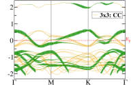
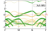
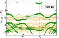
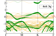
VIII Band structures
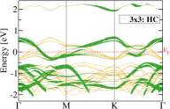
In view of further exploration of the stripe phase and the vs periodicity, we analyse the band structures for the and CDWs, with reference to Fig. S5, comparing it with the band structure of a unit cell, shown in Fig. S4. The calculated band structure of the supercells were unfolded back to the primitive cell Brillouin zone to get an effective band structure of the systems SI-popescu-PRL.104.236403 . This is done following the method of Popescu and Zunger SI-popescu-PRB.85.085201 , which is based on calculating the spectral weights of the supercell eigenvalues and constructing the spectral function. The orange lines in Figs. S5 correspond to the eigenvalues within the Brillouin zone of the supercell (folded), whereas the green curves represent the eigenvalues projected onto the unfolded Brillouin zone with a broadening proportional to their spectral weight. The Nb-derived band crossing the Fermi level features band splittings around M and along K, but the latter is much less pronounced for the CDWs. The valence band below features a splitting along K, MK and M, accompanied to a plethora of valence bands arising from the lattice distortions. Compared to angle resolved photoemission spectroscopic measurements SI-bawden-ncomm2016 ; SI-nakata-NPGAM2016 ; SI-ugeda-nphys2016 ; SI-nakata-NPJ2DMA2018 , these bands look more detailed. The conduction band splitting along M and MK are in agreement; the lower valence band features a two-fold bifurcation at along M and especially K; recent experiments SI-nakata-NPJ2DMA2018 detect such feature along K only, as a result of spin-orbit interaction – which in our calculations is not taken into account.
IX A hint to the properties of a bilayer
Throughout this manuscript, we presented a model for a stripe phase in single layer 1H-NbSe2. Although the stripe phase was not observed for single layers, it was observed for thin films at the surface. As mentioned in the main text, the strain a substrate can apply on a single layer may not be sufficient, or it may be opposite in sign, for the stripe phase to occur. In order to strengthen our argument, we computed the phononic spectra of a bilayer 2H-NbSe2, using a k-mesh of for the wavefunctions and a q-mesh of for the force constants. Due to the centrosymmetry of the 2H-bilayer, instabilities occur along the M line (around 2/3). We modelled bilayers with and periodicities, taking few examples from the single layer case, finding that the energy difference between and lattice distortions ( per unit cell in favour of the periodicity) is in line with the above reported results for the single layer. Although we have not tested all possible configurations, these results suggest that the ordering between and is not highly altered by the symmetry; however, defining a clear trend is not within the scope of the present work. The relaxed structures for the periodicity maintain the same geometry they have in the single layer, whereas the interfaced with a relaxes to a structure; note that the ordering vectors of the two interfaced layers are twisted by with respect to each other, see Fig. S6. The bilayers are not shown because there is no new information about the structure with respect to the single layers.
References
- (1) Arguello, C. J. et al. Visualizing the charge density wave transition in -NbSe2 in real space. Phys. Rev. B 89, 235115 (2014).
- (2) Hofer, W. Challenges and errors: interpreting high resolution images in scanning tunneling microscopy. Prog. Surf. Sci. 71, 147 – 183 (2003).
- (3) Palotás, K. & Hofer, W. A. Multiple scattering in a vacuum barrier obtained from real-space wavefunctions. J. Phys.: Condens. Matter 17, 2705–2713 (2005).
- (4) Mándi, G. & Palotás, K. Chen’s derivative rule revisited: Role of tip-orbital interference in stm. Phys. Rev. B 91, 165406 (2015).
- (5) Tersoff, J. & Hamann, D. R. Theory of the scanning tunneling microscope. Phys. Rev. B 31, 805–813 (1985).
- (6) Soumyanarayanan, A. et al. Quantum phase transition from triangular to stripe charge order in NbSe2. Proc. Natl. Acad. Sci. 110, 1623–1627 (2013).
- (7) Ugeda, M. M. et al. Characterization of collective ground states in single-layer NbSe2. Nat. Phys. 12, 92–97 (2016).
- (8) Chatterjee, U. et al. Emergence of coherence in the charge-density wave state of -NbSe2. Nat. Commun. 6, 6313 (2015).
- (9) Gye, G., Oh, E. & Yeom, H. W. Topological landscape of competing charge density waves in -NbSe2. Phys. Rev. Lett. 122, 016403 (2019).
- (10) Gao, S. et al. Atomic-scale strain manipulation of a charge density wave. Proc. Natl. Acad. Sci. 115, 6986–6990 (2018).
- (11) Nakata, Y. et al. Anisotropic band splitting in monolayer NbSe2: implications for superconductivity and charge density wave. npj 2D Materials and Applications 2, 12 (2018).
- (12) Palotás, K., Mándi, G. & Szunyogh, L. Orbital-dependent electron tunneling within the atom superposition approach: Theory and application to w(110). Phys. Rev. B 86, 235415 (2012).
- (13) Cossu, F. et al. Unveiling hidden charge density waves in single-layer NbSe2 by impurities. Phys. Rev. B 98, 195419 (2018).
- (14) Popescu, V. & Zunger, A. Effective band structure of random alloys. Phys. Rev. Lett. 104, 236403 (2010).
- (15) Popescu, V. & Zunger, A. Extracting versus effective band structure from supercell calculations on alloys and impurities. Phys. Rev. B 85, 085201 (2012).
- (16) Bawden, L. et al. Spin-valley locking in the normal state of a transition-metal dichalcogenide superconductor. Nat. Commun. 7, 11711 (2016).
- (17) Nakata, Y. et al. Monolayer -NbSe2 as a mott insulator. NPG Asia Materials 8, e321 (2016).