present address: QuTech and Kavli Institute of Nanoscience, TU Delft, 2600 GA Delft, The Netherlands
Fast charge sensing of Si/SiGe quantum dots via a high-frequency accumulation gate
Abstract
Quantum dot arrays are a versatile platform for the implementation of spin qubits, as high-bandwidth sensor dots can be integrated with single-, double- and triple-dot qubits yielding fast and high-fidelity qubit readout. However, for undoped silicon devices, reflectometry off sensor ohmics suffers from the finite resistivity of the two-dimensional electron gas (2DEG), and alternative readout methods are limited to measuring qubit capacitance, rather than qubit charge. By coupling a surface-mount resonant circuit to the plunger gate of a high-impedance sensor, we realized a fast charge sensing technique that is compatible with resistive 2DEGs. We demonstrate this by acquiring at high speed charge stability diagrams of double- and triple-dot arrays in Si/SiGe heterostructures as well as pulsed-gate single-shot charge and spin readout with integration times as low as 2.4 s.
keywords:
Charge sensing, quantum dots, spin qubits, reflectometry, silicon, Si/SiGeThe exceptional promise of quantum computation is predicated on scalable hardware that can implement multi-qubit devices as well as efficient methods for qubit readout. In recent years, silicon spin qubits based on electrostatically confined quantum dots (QDs) have been shown to fulfill many of these criteria and are therefore promising building blocks for quantum information applications 1, 2. Due to their low concentration of nuclear-spin-carrying isotopes and established fabrication methods, Si/SiGe heterostructures have particular potential for achieving scalability and fault tolerance 3. While single-qubit 4, 5 and two-qubit 6, 7, 8, 9 operations have been demonstrated with high fidelities, qubit initialization and measurement times are relatively slow. In contrast, in GaAs QD systems, radio-frequency (RF) reflectometry allows fast measurement of charge states 10. Single-shot readout of spin states employs spin-to-charge conversion in combination with a capacitively coupled sensor dot or a nearby quantum point contact 11, 12. Typically, one low-resistance ohmic contact of the sensor is wirebonded to a surface-mount inductor, forming a RF tank circuit that sensitively responds to changes in the sensor resistance and, indirectly, to the qubit’s spin states 12. Singlet and triplet states were distinguished with a signal-to-noise ratio () as high as 6 for integration times as low as 200 ns 13. An application of this technique to accumulation mode silicon devices is possible for carefully designed, high-quality samples 14, but raises specific challenges in contrast to depletion mode GaAs devices: the strong capacitive coupling of the accumulation gate to the 2DEG changes the matching condition of the resonant circuit significantly and, in conjunction with the relatively large 2DEG resistance, impedes RF readout via the sensor’s ohmic contacts. Alternative approaches based on dispersive sensing connect the tank circuit to the plunger gate, such that the reflected RF signal changes when the (quantum) capacitance of the gate electrode changes. This technique, pioneered in GaAs double dots 15 and later applied to silicon devices 16, 17, 18, recently allowed single-shot readout of long-lived states 19, 20, 21, by decreasing the detection bandwidth to the order of kHz. Replacing the off-chip surface-mount inductor by an on-chip high-impedance superconducting resonator significantly increased the single-shot detection bandwidth (0.3 MHz in Ref. 22), but constraints device geometries, materials, and fabrication.
Here, we report high-bandwidth charge sensing compatible with pulsed-gate operation of silicon spin qubits, without the need for nanofabricating additional superconducting elements. We demonstrate this readout technique in undoped Si/SiGe heterostructures, using a single-gate-layer design to form tunable double and triple quantum dot devices. Our reflectometry circuit is galvanically isolated from the heterostructure, by wirebonding a resonating inductor to the accumulation gate of the sensor dot. By decoupling the sensor’s ohmic from the RF ground of the sample board, the reflectometry RF signal effectively becomes sensitive to the sensor’s conductance, rather than only its capacitance. We thereby achieve single-shot charge and spin readout of proximal quantum dots with integration times on the order of a few microseconds.
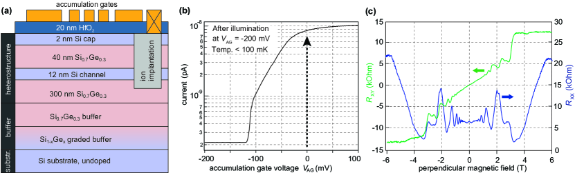
Our quantum dot devices are fabricated from commercially grown, undoped, natural abundance Si/Si0.7Ge0.3 heterostructures, schematically shown in Fig. 1c. Details of the heterostructure, gate fan-out and the fabrication process are provided in the Supporting Information. The Si channel is 42 nm below the gate dielectric, which is grown by atomic layer deposition of HfO2. To avoid a global accumulation gate, a single gate layer patterned by electron-beam lithography defines four large-area accumulation gates and several skinny depletion gates, appropriate to control a triple dot (Fig. 1c) or double dot (Supporting Fig. S2d) with proximal sensor dot. Accumulation gates are operated at positive voltages to accumulate electrons in the 2DEG at the position of the quantum dots, the sensor dot and the source/drain reservoirs. Negative depletion-gate voltages control the electrochemical potential of the dots and thus the electron occupations, as well as the tunnel couplings.
All measurements are performed in a dilution refrigerator with electron temperature below 100 mK. The cryostat is equipped with low-pass filtered twisted pairs (DC lines), attenuated semi-rigid coaxial cables (fast-gate lines), reflectometry hardware (see below), and a superconducting magnet. The undoped quantum wells are insulating at cryogenic temperatures. By temporarily illuminating the chip with a red light-emitting diode while applying a negative gate voltage, a carrier density is subsequently induced at relatively small (positive) accumulation voltages. This effect is also observed in etched Hall bar devices fabricated on the same material, where one gate electrode covers the entire active region (Supporting Fig. S1b). Magnetotransport measurements on such devices confirm the dependence of carrier density on accumulation gate voltage and illumination conditions, and further characterize the quality of the two-dimensional electron gas (see Supporting Fig. S1c for a measurement of quantum Hall plateaus and Shubnikov-de-Haas oscillations). Low-temperature mobilities of up to 105 cm2/Vs are achieved at charge carrier densities around cm-2. The sheet resistivity measures approximately 1.6 k.
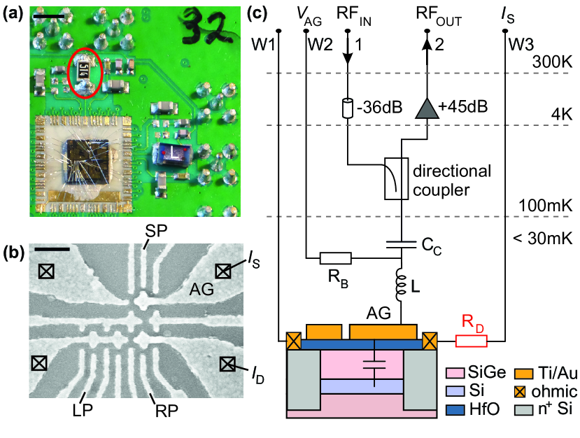
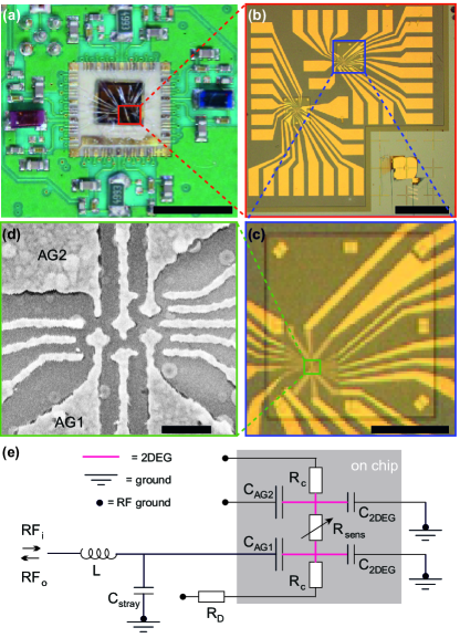
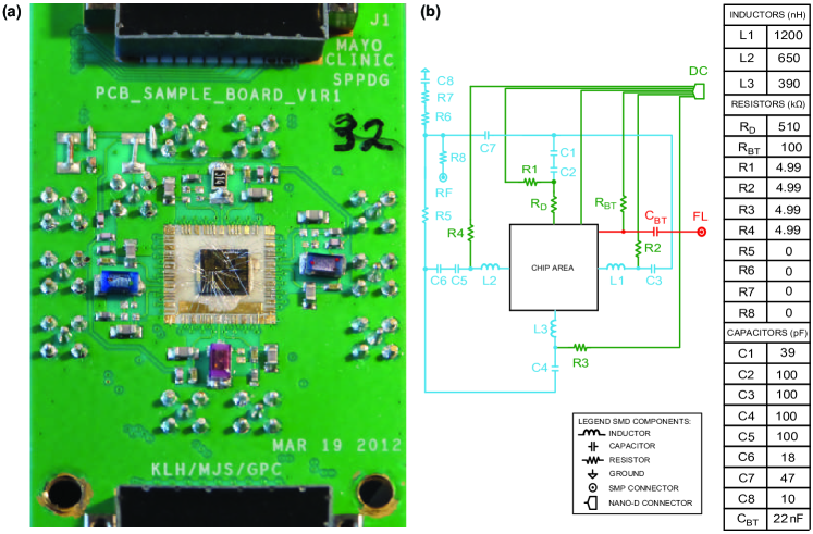
A simplified schematic of our reflectometry readout circuit is shown in Fig. 1c. A surface-mount inductor (L), located on a PCB sample holder (Fig. 1a), is wirebonded to the accumulation gate (AG) of the sensor. The effective capacitance associated with the bond wire (which includes stray capacitance in the PCB and, importantly, a capacitive coupling between the accumulation gate and the underlying 2DEG) and the inductance (1200 nH, Coilcraft 1206CS-122XJEB) forms a RF tank circuit. During reflectometry measurements, a RF carrier is applied to the cryostat, and excites the tank circuit via attenuators ( dB), a directional coupler (-20 dB), and a coupling capacitor (). The tank-circuit response is measured by amplifying the reflected carrier at 4 K (+45 dB, Weinreb CITLF1), followed by homodyne detection at room temperature (Polyphase Microwave quadrature demodulator AD0105B) and sampling of the demodulated voltage () by a fast digitizing card (AlazarTech ATS9440). To prevent the RF excitation from directly shunting to the RF ground of the sample holder, the sensor ohmic underneath the accumulation gate is connected via a high-impedance decoupling resistor ( M) to a DC gate voltage line (W3). The other sensor ohmic is bonded directly to a DC line (W1). A high-impedance bias resistor () allows the application of a tuning voltage () to the accumulation gate.
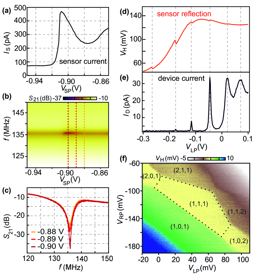
Initially, a sensor dot is tuned up in the top half of the device shown in Fig. 1b, using conventional DC transport measurements via wires W1 and W3. We increase the accumulation gate voltage until a conductive channel is formed, and then operate the barrier gates close to their pinch-off voltage to confine a quantum dot. Figure 2a shows a transport measurement of a Coulomb resonance of the sensor dot as a function of the plunger gate voltage. (In this configuration, we estimate that the resistance between one of the dot’s barriers and the respective wirebonding pads is 20 k, including ohmic contact resistance and finite resistivity of the 2DEG, i.e. a significant fraction of the applied bias voltage drops over the decoupling resistor.) Simultaneously, the demodulated voltage of the reflectometry circuit has been measured as a function of the applied RF frequency (Fig. 2b). The reflected RF power is strongly modulated by the conductance of the sensor dot. The minimum, i.e. when the resonant circuit is matched best, approximately aligns with the Coulomb peak. The resonance frequency stays constant indicating that the capacitive and inductive contributions to the readout circuit are not affected. Fig. 2c compares cuts through (b) at selected gate voltages, showing a resonance dip at 136 MHz. The reflected power at resonance changes by 12 dB, while the current of the sensor dot changes by 170 pA.
By tuning the sensor dot to the flank of a Coulomb peak, the reflected RF amplitude becomes sensitive to the charge within the triple-dot channel. The RF frequency, power and phase are optimized for best readout contrast. First, we tune up a single QD in the triple-dot channel (bottom half of Fig. 1b). A measurement of the sensor reflection as a function of the triple-dot plunger gate voltage is shown in Fig. 2d. The signal shows steps in amplitude that align well with the Coulomb peaks of the triple-dot device measured simultaneously in DC transport (Fig. 2e). In addition, the sensor reflection is sufficiently sensitive to resolve charge transitions in regimes where the DC current through the triple-dot device is below the detection limit (for instance, see the left most charge transition). This is especially relevant for tuning up quantum dot arrays with single-electron occupations, appropriate for many spin qubit experiments. As an example, we tune up a triple QD configuration where each of the QDs is filled with one electron. The charge stability diagram (Fig. 2e) shows the typical pattern of a triple QD. The demodulated voltage is plotted as a function of the left and right plunger gates, as labelled in Fig. 1b.
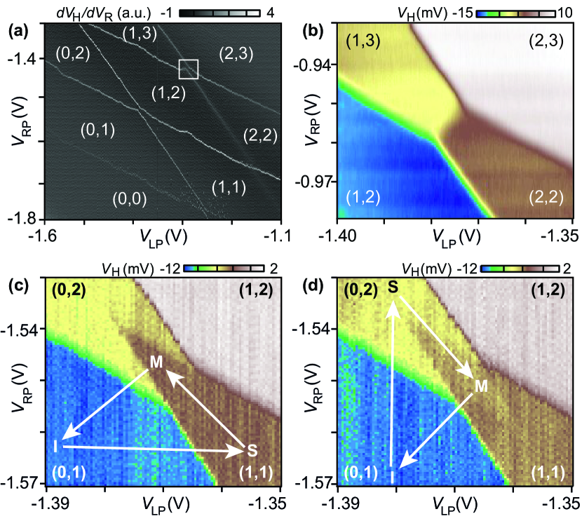
Next, we demonstrate fast device characterization that takes advantage of the high bandwidth of our reflectometry technique. Figure 3a shows the charge stability diagram of a double QD in the low-electron regime (the device is shown in Supporting Fig. S2d). To speed up this acquisition, a 2-kHz saw-tooth pulse is applied to one of the plunger gates while stepping the other. The frequency is chosen to be larger than the cut-off frequency of the bias tee, but smaller than typical tunnel rates to avoid electron latching effects. This technique allows a high-resolution scan of charge stability regions within one second (for example Fig. 3b shows the (1,2), (2,2), (1,3), and (2,3) ground state regions), compared to acquisition times of several minutes using conventional DC transport measurements. At reduced resolution, video rate scans are possible, which facilitates the measurements significantly, especially allowing a “real-time” tuning procedure. The charge stability diagram can then be continuously monitored while adjusting other parameters, such as the tunnel couplings.
Our reflectometry technique also allows pulsed-gate measurements typical of time-domain spin qubit experiments, such as the determination of spin and charge dynamics. In order to determine spin life times directly, nanosecond-to-microsecond-long gate pulses are used, along with spin-to-charge conversion based on Pauli spin blockade, a common readout technique to distinguish between singlet and triplet states 23, 12, 24, 25. To probe these effects in our devices, we apply a three-step pulse cycle to the plunger gates. First, the double QD is initialized in the (0,1) occupation (position I in Fig. 3c), followed by a pulse to separation point (S) where an electron of random spin state is loaded from the reservoir. Readout takes place at the measurement point (M), located in the (0,2) ground state region. A (1,1) singlet state can relax into the energetically favorable (0,2) singlet state, whereas a (1,1) triplet state remains in (1,1) until a spin flip takes place, due to Pauli spin blockade. By applying the RF readout tone only during the M step, the resulting (averaged) reflectometry signal distinguishes between the (0,2) and (1,1) charge states selectively during the M step, and thus provides information about triplet-to-singlet relaxation rates 12.
In Fig. 3c, we record a charge stability diagram while repeatedly applying the pulse cycle described above. The brown region extending from the (1,1) ground state region into the (0,2) ground state region (pulse triangle) shows that the system cannot immediately relax into the (0,2) ground state, indicating the presence of Pauli spin blockade. Thus, the duration of the M step (s) gives a lower bound for the spin relaxation time. In Figure 3d we show a control measurement with an inverted gate pulse trajectory. Here, no such pronounced pulse triangle is visible, in agreement with the expectation that no spin blockade is present in the charge transition from (0,2) to (1,1). Instead, a faint rhombus-shaped region with an average charge between (0,2) and (1,1) appears, likely related to averaging over instrinsic metastabilities within the double dot 26.
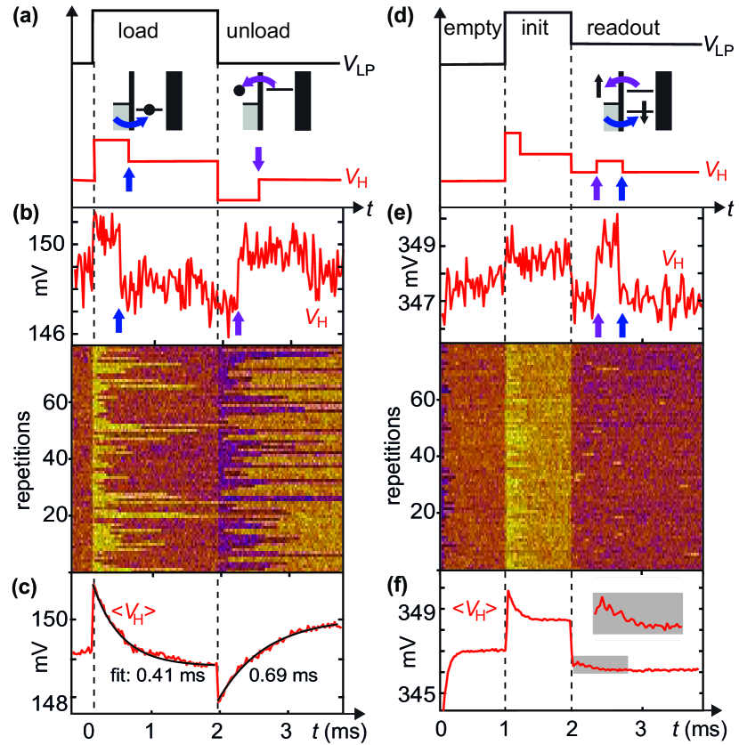
The measurements presented so far were obtained by averaging over multiple pulse cycles. To gain a deeper insight into the dynamics of a system, single-shot measurements are an important technique 11, 27, 28. To show single-shot readout, we apply the RF carrier continuously, and first characterize single-electron charge transitions between a QD and an adjacent reservoir, and focus on spin effects later. For that purpose, we apply a square pulse to the left plunger gate of a triple QD, periodically pulsing the left dot across the 0-1 charge transition to load and unload one electron within each period (see Supporting Fig. S4a). Figure 4a illustrates the applied pulse cycle together with the expected response of the charge sensor signal. The electrostatic effect of one electron entering or leaving the QD manifests itself as a step in the demodulated voltage , as indicated by the arrows. In order to not miss transitions, the pulse period needs to be sufficiently long compared to the characteristic tunneling time. Due to unintentional capacitive coupling between the plunger gates of the triple dot and the sensor dot, also shows steps whenever the plunger voltage changes (black dashed lines).
Figure 4b shows a representative single-shot readout trace from one such pulse cycle, using a pulse period of 3.6 ms and an integration time of 24 s per data point. The arrows highlight the charge sensor response to an electron tunneling in and out from the dot. (Single-shot traces with integration times as small as 2.4 s are discussed in Supporting Fig. S6.) Repeated acquisition of many single-shot traces as in the lower part of Fig. 4b provide statistics of single-electron tunneling times. For example, the average over 200 single-shot traces is shown in Fig. 4c, yielding tunnel in (out) times of 0.41 (0.69) ms from exponential fits for this particular tuning. Alternatively, software detection of tunneling events based on wavelet analysis29 yields tunnel rates in good agreement with those obtained from the exponential fits (see Supporting Figs. S5 and S6).
Finally, we apply a pulse cycle designed to detect spin-dependent tunneling from the QD to the reservoir. The spin degeneracy is lifted by an in-plane magnetic field of 800 mT. We apply a three-step pulse cycle consisting of an empty, initialization and readout step 11, as illustrated in Fig. 4d. First, the energy of both spin states is raised above the Fermi level of the reservoir to empty the QD. Then, the initialization step pulses both states below the Fermi level to load an electron of random spin orientation. Subsequently, spin-selective tunneling is achieved if the readout pulse places the Fermi level just between the Zeeman-split spin states of the QD: A spin-down electron will remain on the QD, while a spin-up electron can tunnel out to the reservoir before a spin-down electron repopulates the QD. The characteristic "electron out electron in" tunneling events associated with spin up show up as a temporary change in the sensor response, as illustrated with arrows in Fig. 4d. Spin-selective tunneling requires the plunger gate voltage in the readout step be chosen correctly, such that spin-split QD states straddle the Fermi level. We tuned to this readout position by repeatedly applying the three-step pulse cycle while slowly stepping the DC gate voltage of the plunger gate until the readout characteristics were observed (see Supporting Fig. S4). For this procedure to work, the Zeeman splitting (eV) needs to exceed the thermal energy (eV), a condition which is fulfilled in the experiment.
Figure 4e shows a single-shot trace representative for a spin-up QD, with the readout step beginning at 2 ms. The out-in tunneling events can be clearly seen in the charge sensor response (arrows). With a rms noise level of 0.42 mV in and a step height of 2.0 mV, the signal-to-noise ratio associated with a 24-s integration time is , corresponding to an effective charge sensitivity of . Assuming that the power signal-to-noise ratio () scales linearly with the integration time, we estimate a minimum integration time s to achieve 22. The 2D plot shows data for 80 repetitions of the same pulse cycle; as expected, some shots show no in-out tunneling events and some of them do. The analysis of spin-down and spin-up traces can be automated using simple thresholding methods, leading to reliable results only at sufficiently high signal-to-noise ratios. An alternative technique, which has been found to be more robust against low-frequency noise and signal drift, is based on wavelet edge detection 29. An example of such a wavelet analysis is shown in Supporting Fig. S6. Alternatively, the presence of spin-up occupations shows up as a "spin bump" when averaging over many single-shot traces (see inset to Fig. 4d), with the shape of the spin bump governed by the tunneling rates 30.
In this work, we demonstrated a high-frequency single-shot readout technique compatible with multi-quantum-dot spin-qubit devices, which we fabricated via a single-layer gate stack in undoped Si/Si0.7Ge0.3 heterostructures. By connecting a surface-mount inductor to the accumulation gate of a sensor dot, while decoupling the sensor ohmic from the RF ground of the sample holder, we were able to make the resonant circuit response sensitive to the sensor conductance, rather than only its quantum capacitance. This allows charge stability diagrams to be acquired at high rates, which significantly speeds the tuning of QD arrays and opens the door to automated tuning procedures. We achieve single-shot charge and spin readout at integration times on the order of a few s, which makes this technique applicable to spin qubit readout. The presented technique constitutes a viable alternative to single-shot readout based on dispersive gate sensing, which so far has been limited to a few kHz or has required integration with millimeter-scale nanofabricated on-chip superconducting resonators. Finally, we expect that this technique is not limited to Si/SiGe devices and spin qubits, but will also find wider application for other accumulation mode devices, for example silicon MOS or germanium hole quantum dot devices.
Competing interests
The authors declare no competing financial interest.
Acknowledgement
We thank Michael Shea for help in developing the PCB sample holder for pulsed reflectometry measurements. We are grateful for Frederico Martins and Filip Malinowski for experimental help and fruitful discussions. This project has received funding from the European Union’s Horizon 2020 research and innovation programme under grant agreement MOSQUITO (No. 688539) and under the Marie Sklodowska-Curie Action Spin-NANO (Nanoscale solid-state spin systems in emerging quantum technologies, Grant Agreement No. 676108), and from the European Union through the FP7 ICT collaborative project SiSPIN (No. 323841). A.C. acknowledges support from the EPSRC Doctoral Prize Fellowship and the Yusuf Ali Travel Bursary.
References
- Loss and DiVincenzo 1998 Loss, D.; DiVincenzo, D. P. Quantum computation with quantum dots. Phys. Rev. A 1998, 57, 120–126
- Vandersypen et al. 2017 Vandersypen, L. M. K.; Bluhm, H.; Clarke, J. S.; Dzurak, A. S.; Ishihara, R.; Morello, A.; Reilly, D. J.; Schreiber, L. R.; Veldhorst, M. Interfacing spin qubits in quantum dots and donors - hot, dense and coherent. npj Quantum Inf. 2017, 3, 34
- Zwanenburg et al. 2013 Zwanenburg, F. A.; Dzurak, A. S.; Morello, A.; Simmons, M. Y.; Hollenberg, L. C. L.; Klimeck, G.; Rogge, S.; Coppersmith, S. N.; Eriksson, M. A. Silicon quantum electronics. Rev. Mod. Phys. 2013, 85, 961–1019
- Kawakami et al. 2014 Kawakami, E.; Scarlino, P.; Ward, D. R.; Braakman, F. R.; Savage, D. E.; Lagally, M. G.; Friesen, M.; Coppermisth, S. N.; Eriksson, M. A.; Vandersypen, L. M. K. Electrical control of a long-lived spin qubit in a Si/SiGe quantum dot. Nat. Nanotech. 2014, 9, 666–670
- Yoneda et al. 2018 Yoneda, J.; Takeda, K.; Otsuka, T.; Nakajima, T.; Delbecq, M. R.; Allison, G.; Honda, T.; Kodera, T.; Oda, S.; Hoshi, Y.; Usami, N.; Itoh, K. M.; Tarucha, S. A quantum-dot spin qubit with coherence limited by charge noise and fidelity higher than 99.9%. Nat. Nanotech. 2018, 13, 102–106
- Veldhorst et al. 2015 Veldhorst, M.; Yang, C. H.; Hwang, J. C. C.; Huang, W.; Dehollain, J. P.; Muhonen, J. T.; Simmons, S.; Laucht, A.; Hudson, F. E.; Itoh, K. M.; Morello, A.; Dzurak, A. S. A two-qubit logic gate in silicon. Nature 2015, 526, 410–414
- Huang et al. 2019 Huang, C.-H.; Yang, C. H.; Chen, C.-C.; Dzurak, A. S.; Goan, H.-S. High-fidelity and robust two-qubit gates for quantum-dot spin qubits in silicon. Phys. Rev. A 2019, 99, 042310
- Zajac et al. 2018 Zajac, D. M.; Sigillito, A. J.; Borjans, F.; Tazylor, J. M.; Burkard, G.; Petta, J. R. Resonantly driven CNOT gate for electron spins. Science 2018, 359, 439–442
- Watson et al. 2018 Watson, T. F.; Philips, S. G. J.; Kawakami, E.; Ward, D. R.; Scarlino, P.; Veldhorst, M.; Savage, D. E.; Lagally, M. G.; Friesen, M.; Coppermisth, S. N.; Eriksson, M. A.; Vandersypen, L. M. K. A programmable two-qubit quantum processor in silicon. Nature 2018, 555, 633–637
- Reilly et al. 2007 Reilly, D. J.; Marcus, C. M.; Hanson, M. P.; Gossard, A. C. Fast single-charge sensing with a rf quantum point contact. Applied Physics Letters 2007, 91, 162101
- Elzerman et al. 2004 Elzerman, J. M.; Hanson, R.; Willems van Beveren, L. H.; Witkamp, B.; Vandersypen, L. M. K.; Kouwenhoven, L. P. Single-shot read-out of an individual electron spin in a quantum dot. Nature 2004, 403, 431–435
- Barthel et al. 2010 Barthel, C.; Kjærgaard, M.; Medford, J.; Stopa, M.; Marcus, C.; Hanson, M.; Gossard, A. Fast sensing of double-dot charge arrangement and spin state with a radio-frequency sensor quantum dot. Phys. Rev. B 2010, 81, 161308
- Higginbotham et al. 2014 Higginbotham, A. P.; Kuemmeth, F.; Hanson, M. P. Coherent Operations and Screening in Multielectron Spin Qubits. Physical Review Letters 2014, 112, 026801
- Takeda et al. 2016 Takeda, K.; Kamioka, J.; Otsuka, T.; Yoneda, J.; Nakajima, T.; Delbecq, M. R.; Amaha, S.; Allison, G.; Kodera, T.; Oda, S.; Tarucha, S. A fault-tolerant addressable spin qubit in a natural silicon quantum dot. Science Advances 2016, 2, e1600694–e1600694
- Petersson et al. 2010 Petersson, K. D.; Smith, C. G.; Anderson, D.; Atkinson, P.; Jones, G. A. C.; Ritchie, D. A. Charge and Spin State Readout of a Double Quantum Dot Coupled to a Resonator. Nano Letters 2010, 10, 2789–2793
- Betz et al. 2015 Betz, A. C.; Wacquez, R.; Vinet, M.; Jehl, X.; Saraiva, A. L.; Sanquer, M.; Ferguson, A. J.; Gonzalez-Zalba, M. F. Dispersively Detected Pauli Spin-Blockade in a Silicon Nanowire Field-Effect Transistor. Nano Lett. 2015, 15, 4622–4627
- Rossi et al. 2017 Rossi, A.; Zhao, R.; Dzurak, A. S.; Gonzalez-Zalba, M. F. Dispersive readout of a silicon quantum dot with an accumulation-mode gate sensor. Appl. Phys. Lett. 2017, 110, 212101
- Crippa et al. 2018 Crippa, A.; Ezzouch, R.; Apra, A.; Amisse, A.; Hutin, L.; Bertrand, B.; Vinet, M.; Urdampilleta, M.; Meunier, T.; Sanquer, M.; Jehl, X.; Maurand, R.; De Franceschi, S. Gate-reflectometry dispersive readout of a spin qubit in silicon. ArXiv:1811.04414 2018,
- 19 Urdampilleta, M. et al. Gate-based high fidelity spin readout in a CMOS device. Nature Nanotech., DOI:10.1038/s41565-019-0443-9
- Pakkiam et al. 2018 Pakkiam, P.; Timofeev, A. V.; House, M. G.; Hogg, M. R.; Kobayashi, T.; Koch, M.; Rogge, S.; Simmons, M. Y. Single-Shot Single-Gate rf Spin Readout in Silicon. Phys. Rev. X 2018, 8, 041032
- West et al. 2019 West, A.; Hensen, B.; Jouan, A.; Tanttu, T.; Yang, C. H.; Rossi, A.; Gonzalez-Zalba, M. F.; Hudson, F. E.; Morello, A.; Reilly, D. J.; Dzurak, A. S. Gate-based single-shot readout of spins in silicon. Nature Nanotech., 2019, 14, 437–441
- Zheng et al. 2019 Zheng, G.; Samkharadze, N.; Noordam, M. L.; Kalhor, N.; Brousse, D.; Sammak, A.; Scappucci, G.; Vandersypen, L. M. K. Rapid high-fidelity gate-based spin read-out in silicon. ArXiv:1901.00687 2019,
- Johnson et al. 2005 Johnson, A. C.; Petta, J. R.; Marcus, C. M.; Hanson, M. P.; Gossard, A. C. Singlet-triplet spin blockade and charge sensing in a few-electron double quantum dot. Phys. Rev. B. 2005, 72, 165308
- Borselli et al. 2011 Borselli, M. G.; Eng, K.; Croke, E. T.; MAune, B. M.; Huang, B.; Ross, R. S.; Kiselev, A. A.; Deelman, P. W.; Alvarado-Rodriguez, I.; Schmitz, A. E.; Sokolich, M.; Holabird, K. S.; Hazard, T. M.; Gyure, M. F.; Hunter, A. T. Pauli spin blockade in undoped Si/SiGe two-electron double quantum dots. Appl. Phys. Lett. 2011, 99, 063109
- Urdampilleta et al. 2015 Urdampilleta, M.; Chatterjee, A.; Lo, C. C.; Kobayashi, T.; Mansir, J.; Barraud, S.; Betz, A. C.; Rogge, S.; Gonzalez-Zalba, M. F.; Morton, J. J. L. Charge Dynamics and Spin Blockade in a Hybrid Double Quantum Dot in Silicon. Phys. Rev. X 2015, 5, 031024
- Biesinger et al. 2015 Biesinger, D. E. F.; Scheller, C. P.; Braunecker, B.; Zimmerman, J.; Gossard, A. C.; Zumbühl, D. M. Intrinsic Metastabilities in the Charge Configuration of a Double Quantum Dot. Physical Review Letters 2015, 115, 106804
- Barthel et al. 2009 Barthel, C.; Reilly, D.; Marcus, C.; Hanson, M.; Gossard, A. Rapid Single-Shot Measurement of a Singlet-Triplet Qubit. Phys. Rev. Lett. 2009, 103, 160503
- Prance et al. 2012 Prance, J. R.; Shi, Z.; Savage, D. E.; Lagally, M. G.; Schreiber, L. R.; Vandersypen, L. M. K.; Friesen, M.; Joynt, R.; Coppersmith, S. N.; Eriksson, M. A. Single-Shot Measurement of Triplet-Singlet Relaxation in a Si/SiGe Double Quantum Dot. Phys. Rev. Lett. 2012, 108, 046808
- Prance et al. 2015 Prance, J. R.; van Bael, B. J.; Simmons, C. B.; Savage, D. E.; Lagally, M. G.; Friesen, M.; Coppersmith, S. N.; Eriksson, M. A. Identifying single electron charge sensor events using wavelet edge detection. Nanotechnology 2015, 26, 215201
- Hayes et al. 2009 Hayes, R. R.; Kiselev, A. A.; Borselli, M. G.; Bui, S. S.; Croke, E. T.; Deelman, P. W.; Maune, B. M.; Milosavljevic, I.; Moon, J.-S.; Ross, R. S.; Schmitz, A. E.; Gyure, M. F.; Hunter, A. T. Lifetime measurements (T1) of electron spins in Si/SiGe quantum dots. ArXiv:0908.0173 2009,
1 Supporting Information for
Fast charge sensing of Si/SiGe quantum dots via a high-frequency accumulation gate
Supporting Information is provided on heterostructure characterization, device fabrication, printed circuit boards, finding the operating point for spin-selective readout, determination of the minimum integration time, and wavelet analysis.
2 Material characterization and device fabrication
A schematic cross section of the device, including the underlying heterostructure, is shown in Fig. S1a. A 300-nm-thick Si0.7Ge0.3 layer is grown on top of a graded buffer in a commercial CVD process, followed by a 12-nm-thick strained Si quantum well, a 40-nm Si0.7Ge0.3 layer and a 2-nm Si cap (Lawrence Semiconductor Research Laboratory Inc.). This places the silicon channel 42 nm below the wafer surface. In order to prevent unwanted accumulation and charge leakage, the wafer has been etched outside the device mesa (visible in Fig. S2c as a 250x250 m square), using an Ar+-ion milling process that removes the top layers of the wafer including the quantum well. Ohmic contacts are created by phosphorus ion implantation (at energies 30 keV and 15 keV, each at a dose of 1x1015 cm-2) followed by a 3-minute activation anneal performed at 700oC. A layer of HfO2 (typically 20 nm) grown by atomic layer deposition is used as the gate dielectric. The gate electrodes are then patterned in a lift-off process, using a single electron-beam-lithography step followed by electron beam evaporation of 3 nm Ti and 20 nm Au.
To perform material characterization, Hall bars were fabricated on the same wafer, following the same fabrication recipe as for the quantum dot devices, and characterized at millikelvin temperatures. Figure S1b shows the transfer characteristics (after the device has been illuminated with a red LED as described in the main text), demonstrating the presence of carriers already at zero accumulation gate voltage. Standard Hall bar measurements are used to determine density and mobility. Figure S1c shows representative magnetotransport data, in which quantization of the Hall resistance and Shubnikov-de Haas oscillations in the longitudinal resistance are clearly visible.
3 Mesa and PCB for accumulation-gate-based sensing
Figure S2a shows the central part of the PCB sample holder with a bonded device chip. The LC resonant circuit used for radio-frequency reflectometry measurements is formed by a commercial SMD inductor (Coilcraft 1206CS series) and the stray capacitance associated with the bond wire (approx. =1.2 pF) connected to the inductor. The bond wire connects to the bonding pad associated with the accumulation gate of the sensor dot, and capacitively couples to the underlying 2DEG (and proximal metallic structures on the chip and PCB). In the case of Fig. S2a, two inductors with different values (typically in the range =390-1200 nH) are visible (purple and blue SMD component), which allow frequency-multiplexed readout of multiple sensor dots. The bonding pad associated with the ohmic contact underlying the accumulation gate is wirebonded to a SMD resistor ( M, green SMD component), to decouple the RF signal from the RF ground of the sample holder (see caption to Fig. S2e). The optical micrograph in Fig. S2b shows a quarter of the chip with two independent devices, each located on its own mesa (one of these mesas is visible in Fig. S2c as a raised square region). A close-up of the fine gate electrodes, in this case a sensor dot next to the double quantum dot used for measurements in Fig. 3, can be seen on the scanning electron micrograph in Fig. S2d.
4 Readout circuit for reflectometry
Figure S3 shows a photograph and a simplified circuit diagram of the printed circuit board (PCB) designed for spin qubit experiments. It comprises 48 DC voltage lines and 10 bias tees (cut-off frequency 70 Hz). Each bias tee allows the combination of a low-frequency tuning voltage (DC) and a high-frequency manipulation voltage (FL, typically carrying millisecond-to-nanosecond voltage pulses) to be applied to the same wirebonding pad. The default PCB configuration can be fitted with up to four SMD inductors, such that a single SMP high-frequency connector (RF) is capacitively coupled to up to four resonant LC circuits, each of them equipped with a bias tee to bias and read out up to four charge sensors via frequency multiplexing. To demonstrate the reflectometry readout method described in the main text, we first modified the circuit by replacing one of the inductors by a decoupling resistor , as shown in Fig. S3b. The accumulation gate of the sensor dot is bonded to one of the resonant circuits (L1), and biased via R2, while the ohmic contact underlying the accumulation gate is bonded to the decoupling resistor (and biased as needed via R1). For later experiments, we also replaced L3 by a decoupling resistor (as shown in Fig. S2a), which allows frequency-multiplexed readout of two devices.
5 Optimization of spin-selective readout point
Figure S4 shows supplementary data related to Figure 4 of the main text, describing how the position in gate voltage space for spin-selective readout was found. For these measurements, a triple-dot device is tuned up as a double-dot device. The double dot (0,0)-(1,0) charge transition is first identified using a charge stability diagram (Fig. S4a). We then apply the pulse cycle for spin-selective readout to the high-frequency connector associated with the left plunger gate, while we step its DC gate voltage (Fig. S4b). If the gate voltage is far too low ( mV) or far too high ( mV), no tunneling events are observed, indicating that the pulse never crosses the charge addition line and the system remains always either in the (0,0) or (1,0) state. In the range mV, the gate voltage is too low and the electron can always tunnel out to the reservoir during the readout step, independent of its spin. In the range mV, the electron cannot tunnel out during readout. Only in a small voltage range set by the Zeeman splitting, the spin-split states of the QD straddle the Fermi level of the reservoirs, such that only spin-up electrons can tunnel out from the dot during readout step. This phenomenological procedure was used to determine the readout point for spin-selective readout.
6 Wavelet edge detection
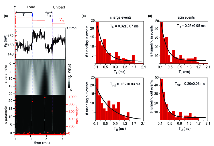
Figure S5 shows the application of a wavelet edge analysis algorithm to data of Fig. 4, allowing automated detection of single-electron-tunneling events as outlined by Prance et al. 29. The technique is based on Canny’s edge detection algorithm, used for the recognition of edges in images, and is well suited to detect sharp edges associated with sensor signals. In order to obtain the function W(t,s), the signal (black trace in S5a) is convolved with a scaled mother wavelet, namely the derivative of a Gaussian function of first order, for different scaling factors s of the wavelet function. During the second step, shown in the fourth row of S5a, the algorithm identifies the track weight for every local minima and maxima at the smallest wavelet scaling factor. The final weight is obtained by summing over the single weights obtained for increasing scaling s, for each trace point. The weight is defined as W(t,s)2 normalized by the median value of W(t,s)2 at a fixed scale.
When the track weight rises above a certain threshold value, here defined as seven times the standard deviation from the average track weight, the event is classified as an edge event. The algorithm is implemented in Igor, with wavelet transformation performed using the Igor CWT function, while the main code is based on MATLAB routines found in the WaveLab850 library (https://statweb.stanford.edu/~wavelab/). Panels S5b,c show the tunneling times obtained by applying the wavelet edge detection to the repeated acquisitions presented in the main text (Fig. 4c,f), for charge and spin events respectively.
In order to determine the charge tunneling rates, each single-shot trace is split into two segments, one for each pulse segment. If only one edge is detected within each of these segments, it is recorded as a tunneling event, i.e. either as a loading time () or unloading time (), depending on whether it occurs in the load or unload segment. The tunneling times are then binned into histograms, using a bin size of 0.1 ms and binning range of 0-2.1 ms (Fig. S5b). Fitting exponentials to the histograms (black trace) yields tunneling times consistent with the tunneling times obtained from averaged single-shot traces in Fig. 4c. The experiment in Fig. 4b was performed at high magnetic field (2 T), suggesting that the difference of tunneling times may either be caused by an accidental (near) degeneracy of two orbitals, or by occupation-dependent and gate-voltage-dependent tunneling barriers.
For the extraction of the spin tunneling times, or are defined slightly differently: referring to the pulse cycle of Fig. 4d, is defined as the time elapsed between the beginning of the readout pulse and the tunnel-out event (purple arrow), whereas corresponds to the time elapsed between the tunnel-out event and the tunnel-in event (blue arrow). The result of the wavelet analysis is binned to extract the tunneling times only if two edges are detected during the measurement step (Fig. S5c). In this case, comparable tunneling times are found for or , as expected for singly-degenerate levels in the Zeeman-split quantum dot.
Though both experiments were performed for the 0-1 transition of the left dot, we obtained differing transition rates for charge and spin events, possibly due to a small effective shift in tuning voltages and associated tunneling barriers (data in Fig. 4b and 4e were taken several weeks apart). In addition, the rates obtained in this way have a significant uncertainty, which can be improved by increasing the statistics within the histograms. As a consequence of the conservative thresholding criterion for identifying edge events, only 10% (2%) of the single-shot traces were identified with charge (spin) events. This set can likely be increased by optimizing the thresholding criterion.
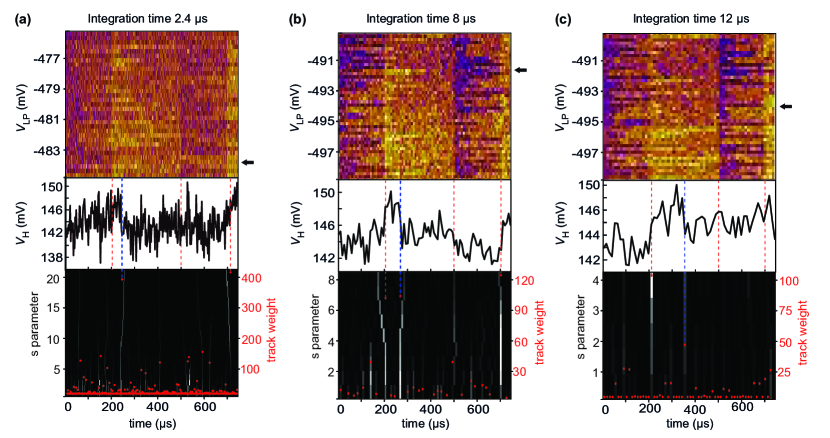
To determine the minimum integration time needed to resolve single-electron-tunneling events, we applied a square pulse to repeatedly induce the 0-1 charge transition, using different settings for the integration time associated with the sampling of single-shot traces (Fig. S6). For an integration time as short as 2.4 s, tunneling events are hard to detect in the raw data by eye (consistent with our estimation of 1 for an integration time of 2.1 s), yet the wavelet edge analysis still yields useful quantitative results.