Tuning the electronic structure and magnetic coupling in armchair B2S nanoribbons using strain and staggered sublattice potential
Abstract
Magnetically-doped two dimensional honeycomb lattices are potential candidates for application in future spintronic devices. Monolayer B2S has been recently unveiled as a desirable honeycomb monolayer with an anisotropic Dirac cone. Here, we investigate the carrier-mediated exchange coupling, known as Ruderman-Kittel-Kasuya-Yoshida (RKKY) interaction, between two magnetic impurity moments in armchair-terminated B2S nanoribbons in the presence of strain and staggered sublattice potential. By using an accurate tight-binding model for the band structure of B2S nanoribbons near the main energy gap, we firstly study the electronic properties of all infinite-length armchair B2S nanoribbons (ABSNRs), with different edges, in the presence of both strain and staggered potential.
It is found that the ABSNRs show different electronic and magnetic behaviors due to different edge morphologies. The band gap energy of ABSNRs depends strongly upon the applied staggered potential and thus one can engineer the electronic properties of the ABSNRs via tuning the external staggered potential. A complete and fully reversible semiconductor (or insulator) to metal transition has been observed via tuning the external staggered potential, which can be easily realized experimentally. A prominent feature is the presence of a quasiflat edge mode, isolated from the bulk modes in the ABSNRs belong to the family , with the width of the ABSNR and an integer number. As a key feature, the position of the quasi-flatbands in the energy diagram of ABSNRs can be shifted by applying the in-plane strains and . At a critical staggered potential ( eV), for nanoribbons of arbitrary width, the quasi-flatband changes to a perfect flatband.
The RKKY interaction has an oscillating behaviour in terms of the applied staggered potentials, such that for two magnetic adatoms randomly distributed on the surface of an ABSNR the staggered potential can reverse the RKKY from antiferromagnetism to ferromagnetism and vice versa. The RKKY in terms of the width of the ribbon has also an oscillatory behavior. It is shown that the magnetic interactions between adsorbed magnetic impurities in ABSNRs can be manipulated by careful engineering of external staggered potential. Our findings pave the way for applications in spintronics and pseudospin electronics devices based on ABSNRs.
I Introduction
The intriguing prospect of the potential nanoelectronic and optoelectronic applications, which may take advantage of the novel two dimensional (2D) materials with exciting electronic properties, has inspired researchers to explore possibilities of such materials with outstanding characteristics. As a typical two-dimensional material, pristine graphene is one of the most attractive materials due to its outstanding potential applications in many fields K. S. Novoselov (2005), but unfortunately, the lack of a finite band gap in graphene is a major obstacle for using graphene in nanoelectronic and optoelectronic devices. However, a big challenge for graphene science is how to open a substantial band gap for graphene without significantly degrading its excellent outstanding advantages in graphene based nanoelectronic devices X. Li (2008); Y.-W. Son and Louie (2006). In the aspect of nanoelectronic and optoelectronic 2D research, the major issue is the availability of 2D materials with a wide band gap window in their band structure. In this regard, B2S monolayer, an atomically thin layer of boron and sulfur atoms arranged in a honeycomb pattern with perfect planar structure, appears in the research field again, by using global structure search method and first principles calculation combined with tight-binding model Y. Zhao and Wang (2018); P. Li and Yang (2018). It is reported that this new 2D anisotropic Dirac cone material has a Fermi-velocity up to in the same order of magnitude as that of graphene. It is thermally and dynamically stable at room temperature and is a potential candidate for future nanoelectronic applications Y. Zhao and Wang (2018); P. Li and Yang (2018). B2S monolayer is the first pristine honeycomb lattice with a tilted anisotropic Dirac cone structure, stabilized by sulfur atoms in free standing condition. Since boron atom has one electron less than carbon, all the reported 2D boron-based Dirac cone materials have much more complicated geometries in comparison with the pristine honeycomb structure of graphene Szwacki (2007); D. Ciuparu (2004); F. Liu (2010); W. An (2006); M. I. Eremets (2001).
In the last decades, magnetic atoms embedded in a non-magnetic host material have been intensively studied in solid state physics due to their functionalities for application in spintronic devices and magnetic recording media Abanin and Pesin (2011); T. Dietl (2000). Dilute magnetic semiconductors, as potential materials for spintronics and optoelectronics, have been studied since early 90-es. These investigations resulted in establishing a unified picture of the nature of indirect exchange interaction between magnetic adatoms, known as the Ruderman-Kittel-Kasuya-Yosida (RKKY) interaction Ruderman and Kittel (1954); Kasuya (1956); Yosida (1957), mediated by a background of conduction electrons of the host material. In diluted metals and semiconductors it is often the dominating magnetic interaction and has played a key part in the development of magnetic phases, e.g., spiral Zare et al. (2016); Shiranzaei et al. (2017a), spin-glass Abanin and Pesin (2011); Eggenkamp et al. (1995); sui Liu et al. (1987), ferromagnetic (FM) Vozmediano et al. (2005); Brey et al. (2007); D.J. Priour et al. (2004); Matsukura et al. (1998); Ko et al. (2011); Ohno (1998) and antiferromagnetic (AFM) Minamitani et al. (2010); Hsu et al. (2015). This long-range spin-spin interaction leads to spin relevant effects in giant magnetoresistance devices M. N. Baibich and Chazelas (1988); G. Binasch and Zinn (1989), spin filters F. Ye and Su (2010), drives ferromagnetism in heavy rare-earth elements I. D. Hughes (2007) as well as in diluted magnetic semiconductors T. Dietl (2000). It was shown that the RKKY interaction consists of three terms, namely Heisenberg, Ising, and Dzyaloshinskii–Moriya (DM) on the surface of zigzag silicene nanoribbons as well as the three dimensional topological insulators Abanin and Pesin (2011); Zare et al. (2016); J.-J. Zhu and Chang (2011), and the competition between them leads to rich spin configurations. An additional term, namely spin-frustrated has discovered in a three-dimensional Weyl semimetal (WSM) that along with the Dzyaloshinskii-Moriya term lies in the plane perpendicular to the line connecting two Weyl points Hosseini and Askari (2015).
In a spin polarized system Parhizgar et al. (2013a) and a material with multi-band structure Parhizgar et al. (2013b), these oscillations become more complicated than a monotonic oscillation with behavior, where is the wave vector of the electrons (holes) at the Fermi level and is the distance of two magnetic impurities. In addition, it is important to note that the magnitude of the RKKY interaction can be severely affected by the density of states (DOS) at the Fermi level Parhizgar et al. (2013c); Shiranzaei et al. (2017a). Owing to the bipartite nature of the honeycomb sublattice, the RKKY coupling in graphene is highly sensitive to the direction of the distance vector between impurities Sherafati and Satpathy (2011); Parhizgar et al. (2013c). In materials with spin-orbit interaction of Rashba type Shiranzaei et al. (2017b), the exchange interaction depends on the direction of the magnetic moments and, as a result, the RKKY interaction becomes anisotropic Shiranzaei et al. (2017a).
We have recently addressed the problem of isolated magnetic adatoms placed on silicene Zare (2019) and phosphorene M. Zare (2018) sheets as well as on zigzag silicene nanoribbons Zare et al. (2016) and bilayer phosphorene nanoribbons Zare and Sadeghi (2018). In a detailed study, we found that the RKKY interaction in silicene can be written in an anisotropic Heisenberg form for the intrinsic case where the spin coupling could realize various spin models, e.g., the XXZ-like spin model Zare (2019). In another work, it has concluded that the RKKY interaction in the bulk phosphorene monolayer is highly anisotropic and the magnetic ground-state of two magnetic adatoms can be tuned by changing the spatial configuration of impurities as well as the chemical potential varying M. Zare (2018). Importantly, the occurrence of these magnetic phases not only depends on the magnetic impurity concentration, but also on the concentration of free carriers in the host material P. J. T. Eggenkamp and de Jonge (1995).
This effective interaction can also be viewed as an indirect coupling mediated by pure spin current in quantum spin Hall systems, due to the helicity J. Gao and Zhang (2009). This interaction oscillates as a function of the distance between two magnetic adatoms (with wavelength ), due to the sharpness of the Fermi surface. Besides these practical magnetic phases, the RKKY interaction can provide information about the intrinsic properties of the material, since this coupling is proportional to the spin susceptibility of the host system.
In the last decades, dilute magnetic semiconductors have emerged as a research hotspot due to their functionalities for application in spintronic devices and magnetic recording media. Inducing magnetism in otherwise nonmagnetic 2D materials has been a subject of intense research due to the unique physical characteristics originating from 2D confinement of electrons, foe concurrent applications in electronic and optoelectronic devices Zutić et al. (2004); Babar and Kabir (2016); W. Han (2014).
Controllable magnetic properties of nanoribbon-based spintronic devices allow the development of the next generation of magnetic and spintronic devices to be realized, and thus much attention has been focused on determining the magnetic properties of 2D honeycomb nanoribbons Klinovaja and Loss (2013); Zare et al. (2016); Zare and Sadeghi (2018); H. Duan and R.-Q.Wang (2017).
Motivated by the future potential of the honeycomb nanoribbons decorated by magnetic impurities, in this work we have addressed the problem of indirect exchange coupling between localized magnetic moments mediated by the conduction electrons of B2S nanoribbons with armchair-terminated edges. Within the tight-binding model we exploit the Green’s function formalism (GF), to reveal how the RKKY interaction between two magnetic impurities, placed on a B2S nanoribbon, is affected by mechanical strains in the presence of a sublattice staggering potential.
It is found that armchair B2S nanoribbons (ABSNRs) show different electronic and magnetic behaviors due to different edge morphologies. The band gap energy of ABSNRs depends strongly upon the applied staggered potential , and thus one can engineer the electronic properties of the ABSNRs with desirable characteristics via tuning the external staggered potential.
A complete and fully reversible semiconductor (or insulator) to metal transition has been observed via tuning the external staggered potential, which can be easily realized experimentally. Interestingly, for the ABSNRs belong to the family , with the width of the ABSNR and an integer number, one can see that a band gap, in which a quasi-flatband completely detached from the bulk bands, is always observed. As a key feature, the position of the quasi-flatbands in the energy diagram of ABSNRs can be shifted by applying the in-plane strains and . At a critical staggered potential ( eV), for ABSNRs with any width, the quasi-flatband changes to a perfect flatband.
It is shown that the RKKY interaction has an oscillating behaviour in terms of the applied staggered potentials, such that for two magnetic adatoms randomly distributed on the surface of an ABSNR the staggered potential can reverse the RKKY from antiferromagnetism to ferromagnetism and vice versa. Meanwhile, the RKKY interaction has an oscillatory behavior in terms of the width of the ribbon.
This paper is organized as follows: In Sec. II, we introduce the system under consideration, i.e., an armchair-terminated B2S nanoribbon under the influence of strain and staggered potential applied to it. A tight-binding model Hamiltonian for monolayer B2S is presented and then the band spectrum of ABSNRs with different edge configurations, under a staggered potential, have been investigated then, we introduce the theoretical framework which will be used in calculating the RKKY interaction, from the real space Green’s function. After that, we discuss our numerical results for the proposed magnetic doped ABSNRs in the presence of both strain and staggered sublattice potential. Finally, our conclusions are summarized in Sec. III.
II Theory and model
II.1 The RKKY interaction
To study indirect magnetic interaction between two local moments in armchair-terminated B2S nanoribbons, we consider the indirect exchange coupling between magnetic impurities to be of the RKKY form, mediated by the conduction electrons in armchair B2S nanoribbon system. The contact magnetic interaction between the spin of itinerant electrons and two magnetic impurities located at positions and with magnetic moments and is given by
| (1) |
where are the conduction electron spin densities at positions and and is the contact potential between the impurity spins and the itinerant carriers.
Using a second-order perturbation Ruderman and Kittel (1954); Kasuya (1956); Yosida (1957), the effective magnetic interaction between local moments induced by the free carrier spin polarization, the RKKY interaction, which arises from quantum effects, reads as
| (2) |
The RKKY interaction is explained using the static carrier susceptibility, the response of the charge density to a perturbing potential , i.e., , which is given by
| (3) |
The static spin susceptibility can be written in terms of the integral over the unperturbed Green’s function as
| (4) |
where is the Fermi energy. The expression for the susceptibility may be obtained by using the spectral representation of the Green’s function
| (5) |
where is the sublattice component of the unperturbed eigenfunction with the corresponding energy . For a crystalline structure, denotes the band index and spin. Substituting Eq. (5) into Eq. (4), after integration over energy, we will get the result for the RKKY interaction. The analytical background of this approach has been already described in details in previous works Zare et al. (2016); Zare and Sadeghi (2018) and is not rediscussed here. Finally, from those analytical calculations the RKKY interaction can be expressed in the following desired result
| (6) | |||||
where, , is the Fermi function. This is a well-known formula in the linear response theory that is the main equation in this work.
II.2 Armchair B2S nanoribbons
In this section, we reintroduce B2S monolayer to the layered-material family as an anisotropic material for optoelectronic and spintronic applications. Since indirect exchange interaction between magnetic moments is significantly affected by the electronic structure of the host material, tailoring electronic properties of this nanostructure is crucial. To do so, the electronic structures of armchair-terminated B2S nanoribbons are studied using tight-binding model.
As very recently reported Y. Zhao and Wang (2018), the most energetically stable structure of B2S monolayer predicted by using global structure search method and first principles calculation combined with tight-binding model, is shown in Fig.1 from which we can see that the planar 2D structure consists of honeycomb lattices, similar to graphene. This honeycomb structure is a global minimum in the space of all possible 2D arrangements of B2S in which each hexagonal ring is distorted with the bond angles ranging from Å to Å, because B and S atoms have different covalent radii and electronegativities Y. Zhao and Wang (2018); P. Li and Yang (2018).
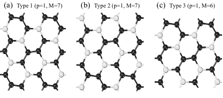
From the Figs.1 (a-c), it has been demonstrated that different types of ribbons are specified by their edge geometry and width. As seen, the armchair B2S nanoribbons can be divided into three families, i.e., (type 1, with boron atoms on the edges of the ABSNR), (type 2, with boron atoms on the edges of the ABSNR), (type 3, with boron atoms on the one edge and boron atoms on the another edge of the ABSNR), with as an integer number. The bottom panel shows an ABSNR of type 1 in which the armchair edge is at the direction. For an infinite-sized ABSNR this system shows translational symmetry along axis. The red-dashed rectangle represents the super unit cell. The usage of such geometry division had two aims, first to evaluate the behaviour of the infinite length ABSNRs, and second to investigate some important finite size effects which will be discussed further.
The geometrical structure of the pristine armchair edge B2S nanoribbon, lying in the plane, is depicted in Fig.1 (d). As shown in this figure, each hexagon consists of four atoms and two atoms, with an orthogonal primitive cell with a space group of and a point group . As shown in Fig.1, the bonding length between two adjacent atoms (- bonds) was calculated to be Å, from the relaxed structure whereas the distances between and atoms (- bonds), are all of the same length Å Y. Zhao and Wang (2018). The black balls correspond to the boron atoms () and the white ones correspond to the sulfur atom (). For simplicity, each atom is labeled with a set , where , represent the and coordinates of the lattice sites. The number of atoms in the vertical zigzag lines across the ABSNRs width, , is used to indicate the width of a BSNR and accordingly we use the number of vertical zigzag lines () to measure its length.
From the analysis of symmetry and orbital characters of the wave functions in a B2S monolayer it is clear that a tight-binding (TB) model involving just the tilted orbitals should be able to describe the band structure of this 2D layered material near the Fermi level Y. Zhao and Wang (2018). We begin with describing this nearest-neighbor effective tight-binding Hamiltonian, given by
| (7) |
with nearest neighbor hopping energies eV and eV Y. Zhao and Wang (2018) (see Fig. 1(d), the bottom panel) where is the annihilation (creation) operator of the electron at the -th lattice site and sums over all nearest neighbor pairs. We consider a general situation where a staggered sublattice potential is applied throughout the sheet, for sublattices , and for sublattices . However, it has been found that the onsite energies for and atoms are eV and eV, respectively and thus, the corresponding parameters , are as follows: for sublattices , and for sublattices , respectively.
Having an accurate tight-binding model, as presented in the equation above (Eq.7), we can numerically calculate the momentum space dispersion of a monolayer armchair nanoribbon of B2S. To do so, we make a one-dimensional (1D) Fourier transform (owing to the translational invariant along the ribbon direction, ), in accordance with Bloch’s theorem obtained from , with respect to the direction:
| (8) |
in which is the unit-cell length along the x-axis. Moreover, and describe coupling within the principal unit cell (intra-unit cell) and between the adjacent principal unit cells (inter-unit cell), respectively based on the real space tight binding model given by Eq.7.
And the real space Hamiltonian can now be written in the desired tridiagonal form:
where and are intra-unit cell and inter-unit cell matrices, respectively.
Furthermore, to understand the effects of the impurity position on the RKKY properties of ABSNRs, we have studied the local density of state (LDOS) of the ABSNRs. Corresponding site-resolved LDOS for site th, at a given position and energy , is obtained from the imaginary part of the Green’s function as , calculated using the unperturbed Green’s function matrix as , where is a positive infinitesimal number.
II.3 Influence of strain and staggered sublattice potentials on the electronic properties of the ABSNRs
The controlled introduction of strain into semiconductors, a key strategy for manipulating the magnetic coupling in 2D nanostructures, has a perfect platform for its implementation in the atomically thin materials in both scientific and engineering applications H. Duan and R.-Q.Wang (2017). Motivated by the search for spintronic materials, a huge number of works have been performed to examine the effectiveness of mechanical strain in modulating the magnetic properties of 2D layered materials Pereira and Neto (2009); F. Liu and Li (2007); V. M. Pereira and Peres (2009); S. R. Power and Ferreira (2012); Peng and Hongbin (2012); F. Guinea and Geim (2010); A. Sharma and Neto (2013); H. Duan and R.-Q.Wang (2017). To gain insight on how B2S nanoribbons can be fruitful in the realization of high-performing magnetic devices, fundamental studies on the strain-induced variation of the electronic and magnetic properties of this new material are essential. In this subsection, the effect of both strain and staggered sublattice potential on the band structure and magnetic exchange interaction is analyzed and discussed. We first consider an armchair B2S nanoribbon lattice in the plane, in the presence of uniaxial strains and while a staggered sublattice potential is applied throughout the ABSNR.
Let the -axis be in the direction of the armchair edge of B2S nanoribbon and the -axis in that of the lateral zigzag edge, as shown in Fig.1. Within the context of continuum mechanics and in the linear deformation regime, application of a uniaxial strain will cause the following change of the bond length , in terms of strain components and
| (15) |
where and denote the positions of an atom before and after deformation, respectively.
In the linear deformation regime, an expansion of the norm of to first order in strains and can be written as where and are the strain-related geometrical coefficients in the ABSNRs. According to the Harrison’s formula the transfer integral () between and orbitals scales with the bond length () as Harrison (1999); H. Tang and Su (2009); Jiang and (2015). By invoking the Harrison’s relationship, we get the following geometrical strain effect on the hopping parameter,
| (16) |
One of the fascinating properties of the new families of 2D layered materials is their possibility to use a staggered potential to manipulate their electronic properties. Motivated by this important problem, we examine the effect of staggered sublattice potential on the electronic structure, by breaking the discrete sublattice symmetry of this honeycomb structure. Here, we investigate the band dispersion of the ABSNRs of infinite length under the influence of the staggered potential.
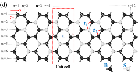
We first present the calculated electronic band structures of ABSNRs superlattices. The energy band structures of infinite length ABSNRs with width of , for different geometry types are plotted in Fig.2. The panels (a),(d) are for ABSNR of type 1, (b),(e) are for type 2, and (c),(f) are for type 3. Top panels are for zero staggered potential () and the bottom ones are for nonzero staggered potentials ( eV). Interestingly, for the ABSNRs of type 2, one can see that a band gap in which a near-midgap band (red curve) completely detached from the bulk bands, is always observed and disappears by introducing staggered sublattice potential term. Indeed, this near-midgap band is shifted and goes away from the flatness mode by applying the staggered potential. As is known, these near-midgap energy bands are due to the edge states whose wave functions are confined near the ABSNR edges H. Zhang (2016); A. Carvalho (2014); H. Guo and Zeng (2014).
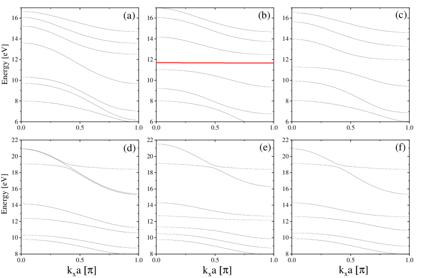
What the Fig. 3 shows is the same as Fig. 2 but for ABSNRs with . As shown, a large electronic band gap is appeared in the band structure of ABSNRs by applying the staggered potential. As can be seen, the resulting band structures are completely different at various values of the strength of the staggered potential. The quasi flatband in the ABSNR of type 2, in the absence of staggered potential (panel (b)), is shown with a red color.
II.4 Quasiflat band tunability in the ABSNRs
Designing the lattice structures which produce the flat band at Fermi energy has attracted much attention recently because of its potential applications in nanoelectronics, and magnetoectronics. The presence of flat bands at Fermi energy gives rise to the large density of states and is responsible for the flat band ferromagnetism K. Nakada (1996); Lieb (1989); Kusakabe and Maruyama (2003); M. Fujita and Kusakabe (1996). There are primarily three ways toward creating flat bands in nanoribbons K. Nakada (1996); Lieb (1989); Kusakabe and Maruyama (2003); M. Fujita and Kusakabe (1996). The modification of zigzag edge by attaching Klein’s bonds gives rises to the partial flat band in Ggraphene nanoribbons. One of simple ways to obtain the flat bands is given by the nonequality between the sublattice sites in bipartite lattices. In such lattices, N-degenerated flat bands appear at the Fermi energy. with , where and are the number of A and B -sublattice sites, respectively Lieb (1989); Fernández-Rossier and Palacios (2007); Ezawa (2008); H. Tamura and Takayanagi (2002). As suggested by Soleimanikahnoj et al., the quasiflat band (midgap-band) modulation provides a platform for pseudospin electronics H. Zhang (2016); A. Carvalho (2014); H. Guo and Zeng (2014), it is interesting to study the band gap and quasiflat band modulation in the ABSNRs.
The aim of this subsection is to elucidate the effect of the both strain and staggered potential on the spectral properties of the quasiflat edge modes in the ribbon geometry of type 2, specially the formation and tunability of the quasiflat bands in the semiconducting gap in the APNRs.
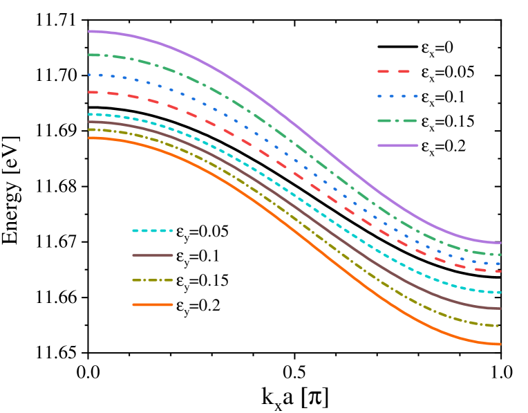
As shown in Fig.4, as a key feature, the position of the quasiflat bands in the energy diagram of APNRs can be shifted by applying the in-plane strains and . Particularly, the quasiflat band energy move up under strains , while shift down with strains .
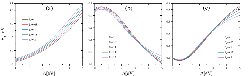
To achieve a superior performance of the ABSNRs in optoelectronic devices based on B2S nanoribbons, a feasible band gap modification is crucial for nanoribbons. To reveal the staggered potential dependence of the band gap of ABSNRs, we have calculated the band gaps for all three types of ABSNR superlattices as a function of the applied staggered potential for different values of strain (see Fig.5). It is visible that the band gap energy of ABSNRs depends strongly upon the applied staggered potential and thus one can engineer the electronic properties of the ABSNRs via tuning the external staggered potential. From the Fig.5 a complete and fully reversible semiconductor (or insulator) to metal transition has been observed via tuning the external staggered potential, which can be easily realized experimentally. It should be emphasized that a negative energy gap corresponds to a metallic state and a positive energy gap corresponds to a semiconductor or insulator electronic state, depending on the energy gap values.
As we have demonstrated, depending on the applied staggered potential in various strain configurations, one may have ABSNRs with favor electronic structure, namely, semiconductor, insulator or the metallic state.
We elaborated more on the potential tunability below and show how to get highly improved flat bands with perfect flatness.
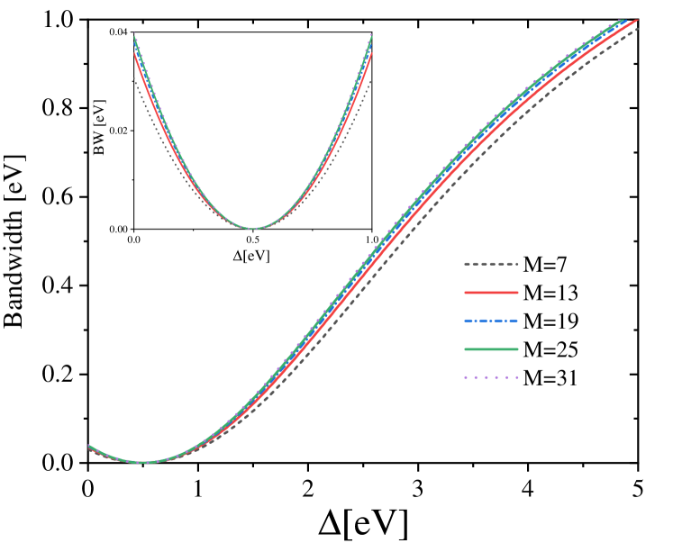
Figure 6 presents the flat band bandwidth versus the applied staggered potential for ABSNRs with different widths. It is clear that, the response of the midgap bands to the applied staggered potential depends on the width of the ribbon. It is worthwhile to note that the bandwidth is generally defined as the energy difference between the upper and lower band edges. It is important to note that at a critical staggered potential ( eV), for ABSNRs with any width, the quasi-flatband changes to a perfect flatband. Moreover, at a fixed staggered potential the midgap bandwidth (MBW) decreases with increasing the width of the ABSNR. Interestingly, the graph of bandwidth for ABSNRs with any width is symmetric with respect to the critical staggered potential (at the interval [0-1] eV), as shown in the inset. For staggered potentials greater than the critical staggered potential (), the bandwidth of the quasi flat bands monotonically increases with increasing the staggered potential. For staggered potentials smaller than the critical staggered potential (), the trend in reverse ı.e., the bandwidth of the bands decreases with increasing the sublattice staggered potentials. As shown, the critical staggered potential (the potential at which semiconductor (or insulator)-to-metal transition occurs) is different for different types of the ABSNRs and changes with strain.
II.5 Numerical results for the RKKY interaction in zigzag B2S nanoribbons
In this section, we present in the following our main numerical results for the numerical evaluation of the RKKY exchange (Eq.6) in the armchair B2S nanoribbons, based on the tight-binding model (Eq.7). For simplicity, all obtained data for the RKKY interaction are multiplied by .
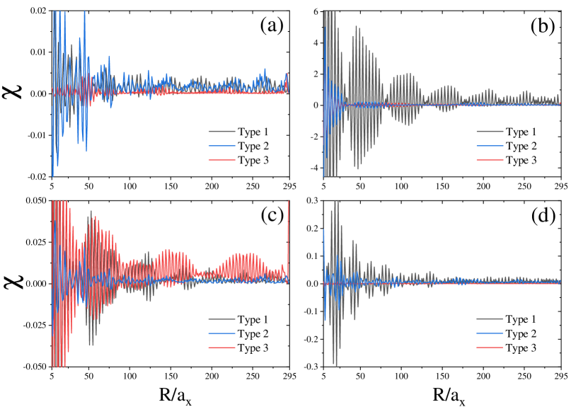
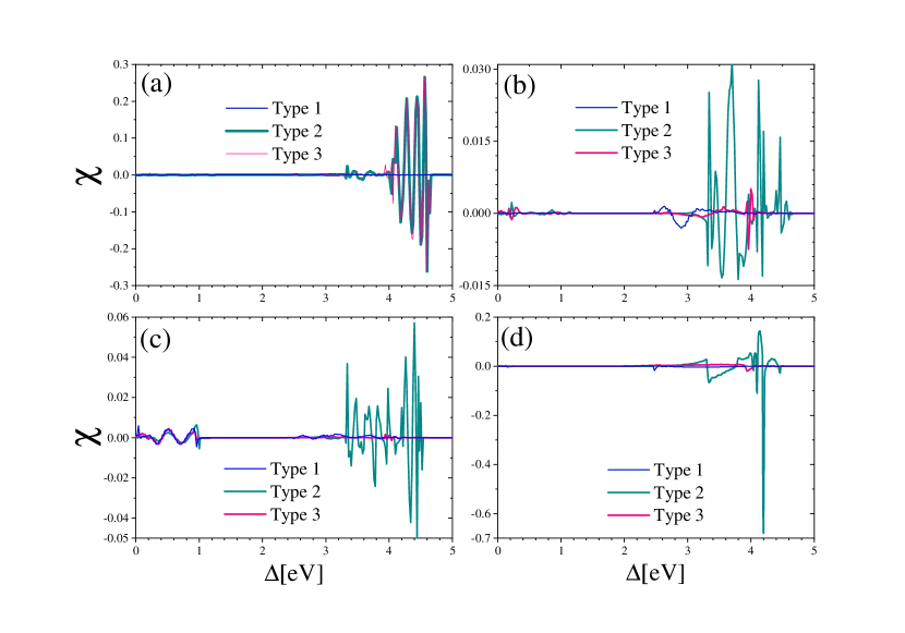
Figure 7 shows the effective exchange interaction for doped ABSNRs ( eV ) with and as a function of distance between the impurities for possible impurity configurations for different types of ABSNRs. The details of the panels are as follows: (a) Both the impurities are located at the same edge, the first impurity at the edge site with coordinate and the second one at lattice sites . (b) Both the impurities are situated in the interior region of the ABSNR, the first impurity at lattice site and the second impurity at lattice points , (c) One impurity is at the edge site and the other one is moved interior of the ABSNR along the line at the lattice sites , and (d) The impurities are located at the opposite edge sites (interedge magnetic coupling) with coordinates and for the types 1 and 2 and and for the ABSNR of types 3.
It is worth pointing out that for small distance between the impurities, the impurities interact very strongly with each other, but then rapidly decay with R until its flattens out to a constant value. As a result, a beating pattern of oscillations of the RKKY interaction occurs for all types of ABSNR, for the doped systems. It is clear that the edge structure of the ABSNRs has a strong effect on the RKKY coupling. The edge-geometry contributions to the RKKY interaction were found to be more important for the geometry with both impurity spins are situated in the interior of the ABSNR (panel (b)), because in this configuration the RKKY interaction is very strong for edge-geometry of type 1 in comparison to the other two geometries. For the case when both spins are inside the ABSNRs (the panel (b)) the result is quite different, because in this situation the RKKY interaction is at least one order of magnitude greater than the other configurations.
The staggered potential dependence of the RKKY interaction is shown in Fig.8, where different distance configurations between two impurities are considered. (a) Both the impurities are located on the same edge at the edge sites with coordinates and (b) Both the impurities are located in the interior of the ABSNR, on lattice points with coordinates and , (c) One of the impurities is located on the edge site and the second one is on the lattice site , and (d) The impurities are located on the opposite edge sites with coordinates and .
It is shown that the RKKY interaction has an oscillating behaviour in terms of the applied staggered potentials, such that for two magnetic adatoms randomly distributed on the surface of an ABSNR the staggered potential can reverse the RKKY from antiferromagnetism to ferromagnetism and vice versa. Importantly, the various edge geometries of ABSNRs show tunability in magnetic RKKY coupling on the application of external staggered potentials, strain. This proves to be an alternative approach to tuning the impurity interactions in ABSNRs.
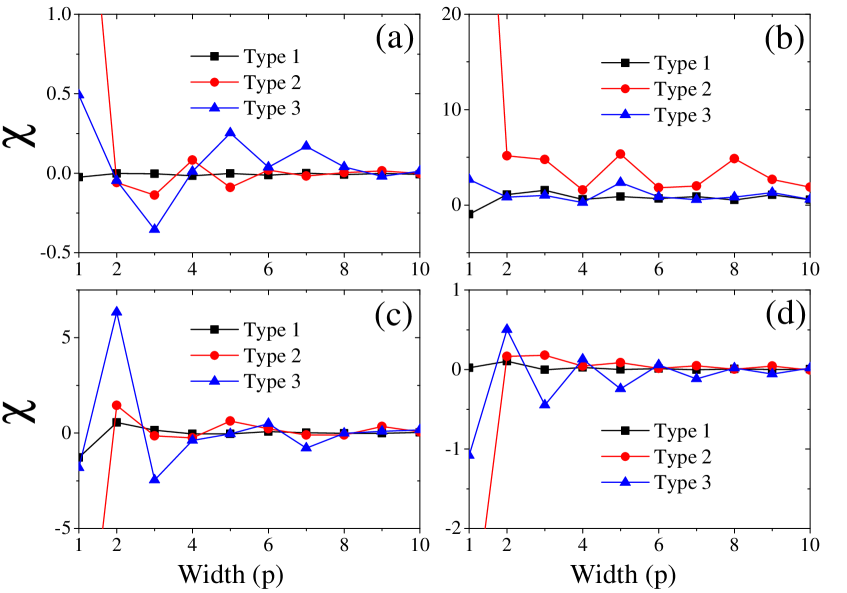
We further investigate the effect of the nanoribbon’s width and edge geometry on the RKKY exchange coupling in ABSNRs (see Fig. 1). Figure 9 shows the dependence of the RKKY coupling on the ribbon width for all three types of ABSNRs. The RKKY interaction has an oscillatory behavior in terms of the width of the ribbon. One can find from these figures that, with an increase in width, the exchange couplings drop at first and then their oscillating amplitudes decay with increasing the width of the ABSNRs finally approach converged value (almost zero). Such an oscillatory behavior versus the ribbon’s width for graphene has been reported previously N. Gorjizadeh and Kawazoe (2008). We observe that for the case that both of two impurities are situated within the interior of the nanoribbon (panel b) the magnetic coupling of ABSNRs with a finite width is always ferromagnetism that is very robust against the impurity movement.
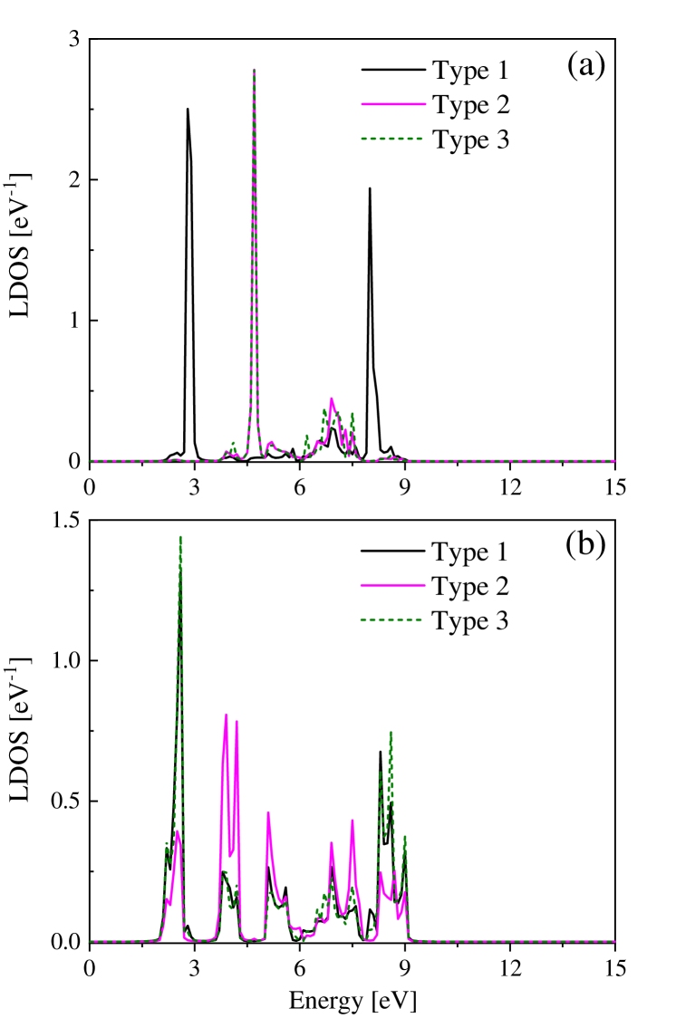
As is known, understanding the sublattice-dependent of local density of states (LDOS) is essential to assess the configuration-dependent exchange interaction. To do so, it is necessary to obtain the diagonal components of the unperturbed Green’s function matrix (), for a lattice site at position and energy E. Fig. 10 illustrates the LDOS for an ABSNR with , , for both edge and bulk sites: (a) an edge lattice site with coordinate and (b) a bulk lattice site with coordinate .
Clearly for ABSNRs of type 2 and type 3, there is a high LDOS peak in the edge sublattice, for energies around eV (panel (a)). Here also two peaks at different energies around and eV appear for ABSNR of type 1. On the contrary, for a bulk site there is a high LDOS peak for energies around eV for ABSNRs of type 1 and type 3 (panel (b)).
III summary
.
To summarize, in this work, we numerically investigate the RKKY exchange coupling between two magnetic impurities located on an armchair B2S nanoribbon, a new anisotropic Dirac cone material, as a strained graphene.
In the first part of our study, employing a tight-binding approach, we investigate the electronic properties of armchair-terminated B2S nanoribbons in the presence of both strain and staggered sublattice potential. It is found that armchair B2S nanoribbons (ABSNRs) show different electronic and magnetic behaviors due to different edge morphologies. The band gap energy of ABSNRs depends strongly upon the applied staggered potential and thus one can engineer the electronic properties of the ABSNRs via tuning the external staggered potential. A complete and fully reversible semiconductor (or insulator) to metal transition has been observed via tuning the external staggered potential, which can be easily realized experimentally. Interestingly, for the ABSNRs belong to the family , with the width of the ABSNR and an integer number, one can see that a band gap, in which a quasi-flatband completely detached from the bulk bands is always observed. As a key feature, the position of the quasi-flatbands in the energy diagram of ABSNRs can be shifted by applying the in-plane strains and . At a critical staggered potential ( eV), for ABSNRs with any width, the quasi-flatband changes to a perfect flatband.
Then, within the tight-binding model we exploit the Green’s function formalism, to reveal how the RKKY interaction between the impurities placed on a ABSNR is affected by mechanical strain, in the presence of a staggering potential. In particular, the effects of ribbon width,strain and staggered sublattice potential on the behavior of RKKY interaction have been investigated. For impurities at fixed values distance, the increase of applied staggered potential leads to higher values of exchange coupling. It is shown that the RKKY interaction has an oscillating behaviour in terms of the applied staggered potentials, such that for two magnetic adatoms randomly distributed on the surface of an ABSNR the staggered potential can reverse the RKKY from antiferromagnetism to ferromagnetism and vice versa. The RKKY interaction has an oscillatory behavior in terms of the width of the ribbon. It is shown that the magnetic interactions between adsorbed magnetic impurities in ABSNRs can be manipulated by careful engineering of external staggered potential. Therefore, the ABSNRs would be expected to be a very promising candidate for spintronics and pseudospin electronics devices based on ABSNRs.
References
References
- K. S. Novoselov (2005) S. V. M. D. J. M. I. K. I. V. G. S. V. D. . A. A. F. K. S. Novoselov, A. K. Geim, Nature 438, 197–200 (2005).
- X. Li (2008) L. Z. S. L. H. D. X. Li, X. Wang, Science 319, 1229–1232 (2008).
- Y.-W. Son and Louie (2006) M. L. C. Y.-W. Son and S. G. Louie, Phys. Rev. Lett. , 97, 216803 (2006).
- Y. Zhao and Wang (2018) J. L. C. Z. Y. Zhao, X. Li and Q. Wang, J. Phys. Chem. Lett. 9, 1815 (2018).
- P. Li and Yang (2018) Z. L. P. Li and J. Yang, J. Phys. Chem. Lett. 9, 4852–4856 (2018).
- Szwacki (2007) N. G. Szwacki, Nanoscale Research Letters 3, 49 (2007).
- D. Ciuparu (2004) Y. Z. L. P. D. Ciuparu, R. F. Klie, J. Phys. Chem. B 108, 13 (2004).
- F. Liu (2010) Z. S. X. D. S. D. J. C. N. X. H. G. F. Liu, C. Shen, J. Mater. Chem. 20 (6267 ), 2197 (2010).
- W. An (2006) Y. G. X. C. Z. W. An, S. Bulusu, J. Chem. Phys. 124, 154310 (2006).
- M. I. Eremets (2001) H.-k. M. R. J. H. M. I. Eremets, V. V. Struzhkin, Science 293 (5528), 272 (2001).
- Abanin and Pesin (2011) D. A. Abanin and D. A. Pesin, Phys. Rev. Lett. 106, 136802 (2011).
- T. Dietl (2000) F. M. J. C. . D. F. T. Dietl, H. Ohno, Science 287, 1019 (2000).
- Ruderman and Kittel (1954) M. A. Ruderman and C. Kittel, Phys. Rev. 96, 99 (1954).
- Kasuya (1956) T. Kasuya, Prog. Theor. Phys. 16, 45 (1956).
- Yosida (1957) K. Yosida, Phys. Rev. 106, 893 (1957).
- Zare et al. (2016) M. Zare, F. Parhizgar, and R. Asgari, Phys. Rev. B 94, 045443 (2016).
- Shiranzaei et al. (2017a) M. Shiranzaei, H. Cheraghchi, and F. Parhizgar, Phys. Rev. B 96, 024413 (2017a).
- Eggenkamp et al. (1995) P. J. T. Eggenkamp, H. J. M. Swagten, T. Story, V. I. Litvinov, C. H. W. Swüste, and W. J. M. de Jonge, Phys. Rev. B 51, 15250 (1995).
- sui Liu et al. (1987) F. sui Liu, W. A. Roshen, and J. Ruvalds, Phys. Rev. B 36, 492 (1987).
- Vozmediano et al. (2005) M. A. H. Vozmediano, M. P. Lopez-Sancho, T. Stauber, and F. Guinea, Phys. Rev. B 72, 155121 (2005).
- Brey et al. (2007) L. Brey, H. Fertig, and S. D. Sarma, Phys. Rev. Lett. 99, 116802 (2007).
- D.J. Priour et al. (2004) J. D.J. Priour, E. H. Hwang, and S. D. Sarma, Phys. Rev. Lett. 92, 117201 (2004).
- Matsukura et al. (1998) F. Matsukura, H. Ohno, A. Shen, and Y. Sugawara, Phys. Rev. B 57, 2037(R) (1998).
- Ko et al. (2011) K. T. Ko, K. Kim, S. B. Kim, H. D. Kim, J. Y. Kim, B. I. Min, J. H. Park, F. H. Chang, H. J. Lin, A. Tanaka, and S. W. Cheong, Phys. Rev. Lett. 107, 247201 (2011).
- Ohno (1998) H. Ohno, Science 281, 951 (1998).
- Minamitani et al. (2010) E. Minamitani, W. A. Dino, H. Nakanishi, and H. Kasai, Phys. Rev. B 82, 153203 (2010).
- Hsu et al. (2015) C.-H. Hsu, P. Stano, J. Klinovaja, and D. Loss, Phys. Rev. B 92, 235435 (2015).
- M. N. Baibich and Chazelas (1988) A. F. F. N. V. D. F. P. P. E. G. C. A. F. M. N. Baibich, J. M. Broto and J. Chazelas, Phys. Rev. Lett. 61, 2472 (1988).
- G. Binasch and Zinn (1989) F. S. G. Binasch, P. Grünberg and W. Zinn, Phys. Rev. B 39, 4828(R) (1989).
- F. Ye and Su (2010) H. Z. F. Ye, G. H. Ding and Z. B. Su, EPL (Europhysics Letters) 90, 47001 (2010).
- I. D. Hughes (2007) A. E. W. H. M. L. J. P. J. B. S. A. S. Z. S. . W. M. T. I. D. Hughes, M. Däne, Nature 446, 650 (2007).
- J.-J. Zhu and Chang (2011) S.-C. Z. J.-J. Zhu, D.-X. Yao and K. Chang, Phys. Rev. Lett. 106, 097201 (2011).
- Hosseini and Askari (2015) M. V. Hosseini and M. Askari, Phys. Rev. B 92, 224435 (2015).
- Parhizgar et al. (2013a) F. Parhizgar, R. Asgari, S. Abedinpour, and M. Zareyan, Phys. Rev. B 12, 125402 (2013a).
- Parhizgar et al. (2013b) F. Parhizgar, H. Rostami, and R. Asgari, Phys. Rev. B 87, 125401 (2013b).
- Parhizgar et al. (2013c) F. Parhizgar, M. Sherafati, R. Asgari, and S. Satpathy, Phys. Rev. B 16, 165429 (2013c).
- Sherafati and Satpathy (2011) M. Sherafati and S. Satpathy, Phys. Rev. B 83, 165425 (2011).
- Shiranzaei et al. (2017b) M. Shiranzaei, F. Parhizgar, J. Fransson, and H. Cheraghchi, Phys. Rev. B 95, 235429 (2017b).
- Zare (2019) M. Zare, Phys. Rev. B (2019).
- M. Zare (2018) R. A. M. Zare, F. Parhizgar, J. Magn. Magn. Mater. 456, 307 (2018).
- Zare and Sadeghi (2018) M. Zare and E. Sadeghi, Phys. Rev. B 98, 205401 (2018).
- P. J. T. Eggenkamp and de Jonge (1995) T. S. V. I. L. C. H. W. S. P. J. T. Eggenkamp, H. J. M. Swagten and W. J. M. de Jonge, Phys. Rev. B 51, 15250 (1995).
- J. Gao and Zhang (2009) X. C. X. J. Gao, W. Chen and F.-C. Zhang, Phys. Rev. B 80, 241302(R) (2009).
- Zutić et al. (2004) I. Zutić, J. Fabian, and S. D. Sarma, Rev. Mod. Phys. 73, 323 (2004).
- Babar and Kabir (2016) R. Babar and M. Kabir, J. Phys. Chem. C 120, 27 (2016).
- W. Han (2014) M. G. J. F. W. Han, R. K. Kawakami, Nat. Nano. 9, 794–807 (2014).
- Klinovaja and Loss (2013) J. Klinovaja and D. Loss, Phys. Rev. B 87, 045422 (2013).
- H. Duan and R.-Q.Wang (2017) S.-H. Z. Z. S. M. Y. H. Duan, S. Li and R.-Q.Wang, New J. Phys. 19, 103010 (2017).
- Pereira and Neto (2009) V. M. Pereira and A. H. C. Neto, Phys. Rev. Lett. 103, 046801 (2009).
- F. Liu and Li (2007) P. M. F. Liu and J. Li, Phys. Rev. B 76, 064120 (2007).
- V. M. Pereira and Peres (2009) A. H. C. N. V. M. Pereira and N. M. R. Peres, Phys. Rev. B 80, 045401 (2009).
- S. R. Power and Ferreira (2012) J. M. D. S. R. Power, P. D. Gorman and M. S. Ferreira, Phys. Rev. B 86, 195423 (2012).
- Peng and Hongbin (2012) F. Peng and W. Hongbin, Phys. B (Amsterdam) 407, 3434 (2012).
- F. Guinea and Geim (2010) M. I. K. F. Guinea and A. K. Geim, Nat. Phys. 6, 30 (2010).
- A. Sharma and Neto (2013) V. N. K. A. Sharma and A. H. C. Neto, Phys. Rev. B 87, 155431 (2013).
- Harrison (1999) W. A. Harrison, (1999).
- H. Tang and Su (2009) B. S. W. H. Tang, J. W.Jiang and Z. B. Su, Solid State Commun. 149, 82 (2009).
- Jiang and (2015) J. W. Jiang and H. S. P. , Phys. Rev. B 91, 235118 (2015).
- H. Zhang (2016) J. H. A. D. Z. C. H. Zhang, Y. Li, Nano Lett. 16, 6124 (2016).
- A. Carvalho (2014) A. N. A. Carvalho, A. Rodin, Europhys. Lett. (EPL) 108 (4), 47005 (2014).
- H. Guo and Zeng (2014) J. D. X. W. H. Guo, N. Lu and X. C. Zeng, J. Phys. Chem. C 118 (25), 14051 (2014).
- K. Nakada (1996) G. D. M. S. D. K. Nakada, M. Fujita, Phys. Rev. B 54, 17954 (1996).
- Lieb (1989) E. Lieb, Phys. Rev. Lett. 62, 1201 (1989).
- Kusakabe and Maruyama (2003) K. Kusakabe and M. Maruyama, Phys. Rev. B 67, 092406 (2003).
- M. Fujita and Kusakabe (1996) K. N. M. Fujita, K. Wakabayashi and K. Kusakabe, J. Phys. Soc. Jpn. 65, 1920 (1996).
- Fernández-Rossier and Palacios (2007) J. Fernández-Rossier and J. J. Palacios, Phys. Rev. Lett. 99, 177204 (2007).
- Ezawa (2008) M. Ezawa, Physica E 40, 1421 (2008).
- H. Tamura and Takayanagi (2002) T. K. H. Tamura, K. Shiraishi and H. Takayanagi, Phys. Rev. B 65, 085324. (2002).
- N. Gorjizadeh and Kawazoe (2008) K. E. N. Gorjizadeh, A. A. Farajian and Y. Kawazoe, Phys. Rev. B 78, 155427 (2008).