Silicon-vacancy color centers in Si- and Si,P-doped nanodiamonds: thermal susceptibilities of photo luminescence band at 740 nm
Abstract
We have characterized thermal susceptibilities of the spectral band at 740 nm of silicon-vacancy (SiV) centers in Si- and Si,P-doped nanodiamonds over a temperature range from 295 K to 350 K, which is of interest for thermometry in biological systems. Si-doped crystals reveal linear dependence of the SiV zero-phonon line position, width and relative amplitude with susceptibilities of 0.0126(4) nm/K, 0.062(2) nm/K and K-1, respectively. Si,P-doped nanodiamonds show significantly smaller (up to 35% for the width) susceptibilities and prove control of SiV properties with additional chemical doping. It is argued that a significant contribution to the heating of the nanodiamonds induced by laser light can be intrinsic due to a high concentration and low luminescence quantum yield of SiV centers.
Minimally invasive temperature sensing with high precision and accuracy is in demand for various applications including cell biologyBaffou et al. (2014). In response, non-invasive optical nanothermometry has emergedJaque and Vetrone (2012); Brites et al. (2012); Vetrone et al. (2010); Kucsko et al. (2013); Plakhotnik, Aman, and Chang (2015); Toyli et al. (2013); Nguyen et al. (2018); Fan et al. (2018); Alkahtani et al. (2018) where temperature is measured ultra locally using fluorescent indicators. Addition of various chemical elements such as nitrogenToyli et al. (2013), siliconNguyen et al. (2018), germaniumFan et al. (2018), and tinAlkahtani et al. (2018) to diamond creates luminescent and thermo-sensitive centers. In particular, silicon-vacancy (SiV) centers have been proposed for all-optical sensingNeu, Agio, and Becher (2012); Jantzen et al. (2016); Li et al. (2016) due to their brightness, photostabilityMerson et al. (2013), and strong, easily detectable at room temperature zero-phonon line (ZPL). Moreover, diamond is a convenient probe delivery vehicle due to its biocompatibilityZhu et al. (2012); Zhang et al. (2013) and easiness of surface functionalizationLiu et al. (2004).
Temperature-dependent luminescence properties of SiV centers have been studiedLagomarsino et al. (2015); Jahnke et al. (2015); Dragounová et al. (2017); Nguyen et al. (2018); Neu et al. (2013), but measured in bulk diamond or in nanodiamonds below room temperatureNeu et al. (2013). Some of the results are also controversial. The reports on optical thermometry with SiV-centers use mostly ZPL peak position for sensingAlkahtani et al. (2018); Nguyen et al. (2018) although multiparametric analysis using other parameters such as ZPL relative amplitude and full-width at half maximum (FWHM) can significantly reduce the noise floor and thus improve the precision of measurementsChoi et al. (2019).
In this Letter, we present temperature-dependent optical characterisation of SiV color centers in nanodiamonds at temperatures from 295 to 350 . We investigate two types of samples: Si-doped and Si,P-doped nanodiamonds. Phosphorus (P) has attracted attention because it was considered as a candidate for n-type doping Koizumi et al. (1998); Prins (1995), even though some reportsJones, Lowther, and Goss (1996) point on drawbacks. Here we test the idea of tuning thermal susceptibility of SiV centers, an important factor affecting precision of the temperature measurements, by adding another impurity to Si-doped diamond.
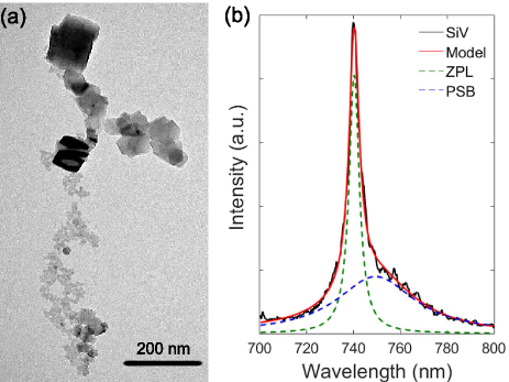
Si- and Si,P-doped nanodiamonds with SiV color centers were obtained by high pressure - high temperature (HPHT) treatment of the catalyst metal-free mixtures of naphthalene - (Chemapol) with tetrakis(trimethylsilyl)sylane – (Stream Chemicals Co.) and naphthalene with tetrakis(trimethylsilyl)sylane and triphenylphosphine – C18H15P (Sigma-Aldrich), respectivelyDavydov et al. (2014). Cold-pressed tablets of the initial homogeneous mixture (5-mm diameter and 4-mm height) were placed into a graphite container, which simultaneously served as a heater of the high-pressure toroid-type apparatus. The experimental procedure consisted of loading the high-pressure apparatus to 8.0 GPa at room temperature, heating the sample to the temperature of diamond formation (1400 ), and short (3-10 s) isothermal exposure of the sample at this temperature. The obtained high-pressure states have been isolated by quenching to room temperature under pressure and then complete pressure release. X-ray diffraction (XRD) and Raman spectroscopy, and transmission electron microscopy were used for preliminary characterization of synthesized diamond materials. The obtained nanodiamond products consist of different particle size distributions. A typical transmission electron microscope (TEM) image of nanodiamonds is shown in Fig. 1(a).
The nanodiamonds were dispersed in de-ionised water, treated with ultrasound (QSonica, Q125) for 30 seconds to break down aggregates and drop-cast on a cover glass for optical characterisation.
Optical properties of the Si- and Si,P-doped nanodiamonds were studied with a home-built microscope. Luminescence of the SiV centers was excited by a 532-nm laser (Cohrernt, Verdi-V5) focused onto a single crystal (an object with a diffraction limited size of the optical image) through an air objective (Nikon, NA = 0.55). The temperature was set using a Peltier element heating/cooling stage (TC-720 Thermoelectric Temperature Controller). The emission collected by the same objective and filtered to reject the excitation light was directed to a spectrometer (Princeton Instruments Acton 2300i). To minimize effects of spatial displacement of the sample (particularly after every change of the stage temperature) on the accuracy of spectral measurements, we employed a grating with 1200 l/mm ruling which provided a large dispersion (about 2.05 nm/mm).
Photo luminescence spectra revealed bands with ZPLs at 740-nm wavelengthFeng and Schwartz (1993) and red-shifted PSBs, Fig. 1(b). The shape of the luminescence band is modeled by a sum of two Lorentzians and a linear background term
| (1) |
Separation of the spectrum into the ZPL and the PSB is ambiguous and the true shape of the two parts is more complicated but Eq. (1) satisfactorily fits the data as can be seen in Fig. 1(b). The following parameters – ZPL width , position , relative amplitude , PSB width , and splitting between ZPL and PSB maxima were extracted from spectra measured at different temperatures by fitting Eq. (1) to the experimental data using a least-squares method. Thermal susceptibility of (similar for other parameters) is defined as follows .
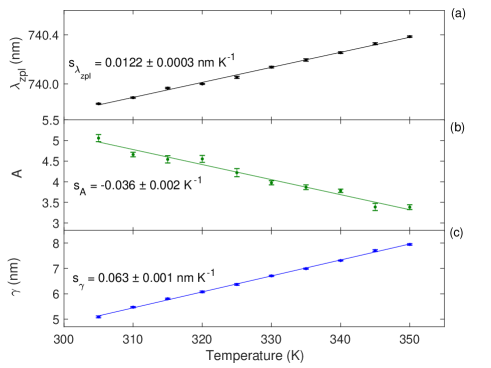
The temperature of the Peltier stage has been variable from 293 K to 318 K with an increment of 5 K but the actual temperature of the nanodiamonds was higher at each setting because of heating caused by the laser light. To take this into account, we measured spectra at two laser powers, 20 mW and 50 mW and the value of has been determined at each power. It has been found that does not depend on laser power or stage temperature within the investigated range and the accuracy of measurements. The difference between at 50 mW and 20 mW and the value of have been used to find for each crystal, the increment of temperature caused by 30-mW increase of the laser power. To obtain the actual crystal temperature at 20 mW and 50 mW, and were added to the stage temperature respectively. As an example, data with corrected temperature are shown in Fig. 2. First four data points are measured at 20 mW (305 K to 320 K), and the remaining six are obtained at 50 mW. Similar procedure has been applied to Si,P-doped diamond. We have summarized all the observations for all measured crystals in Tab. 1 and Tab. 2. These tables also include , the total detected photon count rate at 50 mW.
On average, the temperature increase was about 13 K and 3 K for Si-doped and Si,P-doped nanodiamonds. The origin of heating is not clear but the heat generated directly by SiV centers needs a due consideration. The luminescence quantum yield of SiV centers is about 5% in a CVD diamond filmTurukhin et al. (1996) but it can be several times smaller in nanocrystalsPlakhotnik and Aman (2018). The power of heat released by SiV centers inside a diamond crystal is nW, where quantum yield , photon detection efficiencyChapman and Plakhotnik (2011) , and detected photon count rate MHz. The corresponding steady-state increase of temperature is about 4 K under the assumptions that the heat conductivity coefficient is that of air and the radius of the crystals nm. This is an order of magnitude smaller than the value observed in the experiment but the effective heat conduction from the particle to the air is much smaller than obtained using the bulk value of when the size of the crystal in comparable to the mean free path of air moleculesDaun and Huberman (2012) (about 70 nm). Thermal resistance between the substrate and the crystal may also be significant and dependent on the shape and orientation of the nanocrystal. Thus, it is plausible that not radiative energy release by photo excited SiV centers is responsible for the heating.
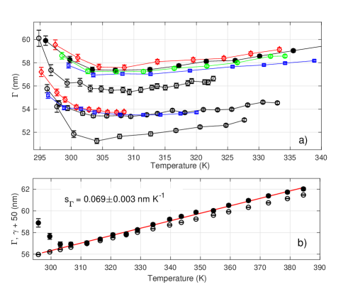
Temperature dependence of two remaining parameters of SiV spectra, the PSB peak position and width were relatively harder to measure accurately. This is because they turned out to be much more affected by small changes in the position of the crystal due to thermal expansion of the stage. To overcome this difficulty, we have used laser power to regulate crystal temperature and kept the stage temperature constant. The results are plotted in Fig. 3 for several nanocrystals showing a common feature, a minimum at approximately 305 K and a nearly linear increase above where the value of nm/K is similar to the value of . The origin of the initial decrease is unclear but positions of the minima in Fig. 3 will not be aligned horizontally if power is used instead of temperature as a Cartesian coordinate in Fig. 3.
Susceptibilities and in Si-doped diamond are consistent within the standard deviation with previous measurements in bulkNguyen et al. (2018); Lagomarsino et al. (2015). Si,P- and Si-doped nanodiamonds show similar while and especially are significantly smaller (up to 35%) in Si,P-doped nanodiamonds. These results prove that additional chemical doping may significantly affect the thermal properties of SiV centers and thus a new direction for research opens up. The sample standard deviations in Si,P-doped nanodiamonds are approximately 3 times larger than in Si-doped samples. A smaller number of SiV centers per crystal in Si,P-doped nanodiamonds as suggested by smaller photon rates can explain the difference. A smaller size of the Si,P-doped nanodiamonds and/or smaller Si concentration (because P and Si atoms are competing for analogous sites in the crystal lattice) are the factors reducing the number of SiV centers.
In summary, we have characterized effects of temperature on luminescent properties of SiV centers in Si- and Si,P-doped nanodiamond samples. In Si-doped crystals and in the temperature range from 305 K to 350 K, susceptibilities , , and are 0.0126(4) nm/K, K-1 and 0.062(2) nm/K, respectively. Simultaneous introduction of Si and P in nanodiamonds affects luminescence spectra of SiV centers and their dependence on temperature. In particular, nm/K, K-1 and nm/K in Si,P-doped crystals. Decrease of is quite significant. Thus temperature susceptibility of SiV centers can be modified by co-doping and further research may identify elements significantly enhancing the temperature response. High concentration of SiV can result in intrinsic heating which should be carefully considered. This work provides comprehensive characterization of luminescent properties of SiV centers in nanodiamonds which are important for optical thermometry especially in the range relevant for biological applications.
The financial support is provided by Human Frontier Science Program, RGP0047/2018. V. D. thanks Russian Foundation for Basic Research (Grant 18-03-00936).
| Si-doped nanodiamond | ||||||||||
| No. | ||||||||||
| nm | nm | nm | nm | K | MHz | |||||
| 1 | 740.179(6) | 0.0114(5) | 7.13(2) | 0.059(2) | 4.47(3) | -0.031(3) | 58.6(8) | 10.0(1) | 23.3 | 46.8 |
| 2 | 740.109(5) | 0.0114(8) | 6.47(1) | 0.059(1) | 4.00(8) | -0.042(6) | 62(1) | 9.4(2) | 23.1 | 34.0 |
| 3 | 740.347(1) | 0.012(1) | 6.44(2) | 0.064(3) | 4.03(2) | -0.033(3) | 66.5(6) | 9.4(2) | 21.9 | 31.8 |
| 4 | 740.053(8) | 0.0131(6) | 6.34(3) | 0.064(2) | 4.22(9) | -0.035(4) | 59(1) | 12.8(1) | 20.0 | 41.0 |
| 5 | 740.238(6) | 0.0130(4) | 6.28(2) | 0.066(1) | 4.34(3) | -0.042(3) | 67.2(5) | 9.9(2) | 19.1 | 40.1 |
| 6 | 740.467(5) | 0.014(1) | 6.82(2) | 0.053(5) | 3.99(2) | -0.037(3) | 62.3(4) | 11.3(1) | 19.9 | 100.9 |
| 7 | 740.256(6) | 0.012(2) | 6.26(1) | 0.066(2) | 4.57(3) | -0.041(4) | 64.0(4) | 13.2(1) | 17.2 | 28.2 |
| 8 | 740.194(7) | 0.0114(4) | 6.04(1) | 0.062(3) | 4.55(3) | -0.032(3) | 64.8(5) | 13.5(1) | 21.2 | 38.9 |
| 9 | 739.872(6) | 0.015(1) | 6.36(1) | 0.067(4) | 4.56(8) | -0.042(5) | 49.3(2) | 11.6(1) | 18.1 | 37.0 |
| 10 | 740.247(3) | 0.0120(6) | 6.70(1) | 0.057(4) | 4.09(6) | -0.035(3) | 49.9(4) | 10.4(1) | 20.9 | 16.8 |
| Mean | 740.20 | 0.0126 | 6.49 | 0.062 | 4.28 | -0.037 | 60.3 | 11.5 | 20.5 | 41.5 |
| std | 0.16 | 0.0013 | 0.32 | 0.0047 | 0.25 | 0.0044 | 6.3 | 1.5 | 2.0 | 22.4 |
| Si,P-doped nanodiamond | ||||||||||
| No. | ||||||||||
| nm | nm | nm | nm | K | MHz | |||||
| 1 | 739.872(3) | 0.015(1) | 6.65(2) | 0.062(4) | 4.54(4) | -0.028(5) | 54.5(8) | 11.4(2) | 6.1 | 0.6 |
| 2 | 739.993(4) | 0.054(7) | 6.38(2) | 0.042(1) | 4.56(5) | -0.033(4) | 33.0(4) | 10.6(1) | 6.9 | 1.8 |
| 3 | 739.848(3) | 0.010(1) | 4.94(1) | 0.037(2) | 6.36(7) | -0.035(4) | 56(1) | 11.6(3) | 2.5 | 5.3 |
| 4 | 739.598(3) | 0.021(2) | 5.34(1) | 0.061(1) | 5.38(5) | -0.027(4) | 57.3(6) | 13.1(2) | 8.5 | 1.8 |
| 5 | 739.771(4) | 0.0145(6) | 4.83(1) | 0.043(2) | 6.31(5) | -0.031(4) | 53.9(5) | 10.7(1) | 4.6 | 5.5 |
| 6 | 740.476(7) | 0.014(2) | 6.93(2) | 0.059(3) | 3.98(3) | -0.022(3) | 43.5(4) | 15.0(1) | 7.7 | 5.9 |
| 7 | 739.639(6) | 0.010(1) | 6.15(1) | 0.033(2) | 5.53(4) | -0.030(3) | 55.7(5) | 13.9(2) | 11.2 | 3.9 |
| 8 | 739.836(6) | 0.014(2) | 5.98(2) | 0.036(4) | 4.03(3) | -0.034(4) | 63(1) | 16.4(3) | - | 0.4 |
| 9 | 740.251(7) | 0.0139(8) | 6.03(1) | 0.048(2) | 4.81(3) | -0.022(3) | 49.2(5) | 11.2(2) | 9.7 | 1.8 |
| 10 | 740.358(7) | 0.0138(6) | 6.25(1) | 0.045(3) | 5.55(7) | -0.029(2) | 54.2(9) | 14.2(1) | 7.8 | 0.4 |
| 11 | 740.238(7) | 0.014(1) | 7.53(1) | 0.049(3) | 4.24(4) | -0.027(3) | 47.3(5) | 10.2(2) | 8.3 | 1.3 |
| 12 | 740.478(8) | 0.013(2) | 6.69(2) | 0.050(2) | 3.92(3) | -0.030(3) | 47.3(5) | 17.2(1) | 7.7 | 5.3 |
| 13 | 739.579(3) | 0.0130(4) | 4.75(1) | 0.045(1) | 6.45(5) | -0.031(3) | 56.6(7) | 13.8(2) | 7.6 | 1.8 |
| 14 | 739.872(2) | 0.0132(6) | 5.09(2) | 0.042(1) | 5.10(5) | -0.032(4) | 53.6(7) | 12.7(2) | 8.0 | 3.8 |
| Mean | 739.0 | 0.014 | 5.96 | 0.046 | 5.05 | -0.031 | 51.9 | 13.0 | 7.4 | 2.8 |
| std | 0.32 | 0.0030 | 0.86 | 0.0091 | 0.90 | 0.0037 | 7.4 | 2.2 | 2.0 | 2.0 |
References
- Baffou et al. (2014) G. Baffou, H. Rigneault, D. Marguet, and L. Jullien, “A critique of methods for temperature imaging in single cells,” Nature Methods 11, 899 (2014).
- Jaque and Vetrone (2012) D. Jaque and F. Vetrone, “Luminescence nanothermometry,” Nanoscale 4, 4301–4326 (2012).
- Brites et al. (2012) C. D. Brites, P. P. Lima, N. J. Silva, A. Millán, V. S. Amaral, F. Palacio, and L. D. Carlos, “Thermometry at the nanoscale,” Nanoscale 4, 4799–4829 (2012).
- Vetrone et al. (2010) F. Vetrone, R. Naccache, A. Zamarrón, A. Juarranz de la Fuente, F. Sanz-Rodriguez, L. Martinez Maestro, E. Martin Rodriguez, D. Jaque, J. García Solé, and J. A. Capobianco, “Temperature sensing using fluorescent nanothermometers,” ACS Nano 4, 3254–3258 (2010).
- Kucsko et al. (2013) G. Kucsko, P. Maurer, N. Y. Yao, M. Kubo, H. Noh, P. Lo, H. Park, and M. D. Lukin, “Nanometre-scale thermometry in a living cell,” Nature 500, 54 (2013).
- Plakhotnik, Aman, and Chang (2015) T. Plakhotnik, H. Aman, and H.-C. Chang, “All-optical single-nanoparticle ratiometric thermometry with a noise floor of 0.3KHz-1/2,” Nanotechnology 26, 245501 (2015).
- Toyli et al. (2013) D. M. Toyli, F. Charles, D. J. Christle, V. V. Dobrovitski, and D. D. Awschalom, “Fluorescence thermometry enhanced by the quantum coherence of single spins in diamond,” Proc. Natl. Acad. Sci. U.S.A 110, 8417–8421 (2013).
- Nguyen et al. (2018) C. T. Nguyen, R. E. Evans, A. Sipahigil, M. K. Bhaskar, D. D. Sukachev, V. N. Agafonov, V. A. Davydov, L. F. Kulikova, F. Jelezko, and M. D. Lukin, “All-optical nanoscale thermometry with silicon-vacancy centers in diamond,” Appl. Phys. Lett. 112, 203102 (2018).
- Fan et al. (2018) J.-W. Fan, I. Cojocaru, J. Becker, I. V. Fedotov, M. H. A. Alkahtani, A. Alajlan, S. Blakley, M. Rezaee, A. Lyamkina, Y. N. Palyanov, et al., “Germanium-vacancy color center in diamond as a temperature sensor,” ACS Photonics 5, 765–770 (2018).
- Alkahtani et al. (2018) M. Alkahtani, I. Cojocaru, X. Liu, T. Herzig, J. Meijer, J. Küpper, T. Lühmann, A. V. Akimov, and P. R. Hemmer, “Tin-vacancy in diamonds for luminescent thermometry,” Appl. Phys. Lett. 112, 241902 (2018).
- Neu, Agio, and Becher (2012) E. Neu, M. Agio, and C. Becher, “Photophysics of single silicon vacancy centers in diamond: implications for single photon emission,” Optics Express 20, 19956–19971 (2012).
- Jantzen et al. (2016) U. Jantzen, A. B. Kurz, D. S. Rudnicki, C. Schäfermeier, K. D. Jahnke, U. L. Andersen, V. A. Davydov, V. N. Agafonov, A. Kubanek, L. J. Rogers, et al., “Nanodiamonds carrying silicon-vacancy quantum emitters with almost lifetime-limited linewidths,” New J. Phys. 18, 073036 (2016).
- Li et al. (2016) K. Li, Y. Zhou, A. Rasmita, I. Aharonovich, and W. Gao, “Nonblinking emitters with nearly lifetime-limited linewidths in cvd nanodiamonds,” Phys. Rev. Appl. 6, 024010 (2016).
- Merson et al. (2013) T. D. Merson, S. Castelletto, I. Aharonovich, A. Turbic, T. J. Kilpatrick, and A. M. Turnley, “Nanodiamonds with silicon vacancy defects for nontoxic photostable fluorescent labeling of neural precursor cells,” Opt. Lett. 38, 4170–4173 (2013).
- Zhu et al. (2012) Y. Zhu, J. Li, W. Li, Y. Zhang, X. Yang, N. Chen, Y. Sun, Y. Zhao, C. Fan, and Q. Huang, “The biocompatibility of nanodiamonds and their application in drug delivery systems,” Theranostics 2, 302 (2012).
- Zhang et al. (2013) X. Zhang, S. Wang, M. Liu, J. Hui, B. Yang, L. Tao, and Y. Wei, “Surfactant-dispersed nanodiamond: biocompatibility evaluation and drug delivery applications,” Toxicol. Res. 2, 335–342 (2013).
- Liu et al. (2004) Y. Liu, Z. Gu, J. L. Margrave, and V. N. Khabashesku, “Functionalization of nanoscale diamond powder: fluoro-, alkyl-, amino-, and amino acid-nanodiamond derivatives,” Chem. Mater. 16, 3924–3930 (2004).
- Lagomarsino et al. (2015) S. Lagomarsino, F. Gorelli, M. Santoro, N. Fabbri, A. Hajeb, S. Sciortino, L. Palla, C. Czelusniak, M. Massi, F. Taccetti, et al., “Robust luminescence of the silicon-vacancy center in diamond at high temperatures,” AIP Advances 5, 127117 (2015).
- Jahnke et al. (2015) K. D. Jahnke, A. Sipahigil, J. M. Binder, M. W. Doherty, M. Metsch, L. J. Rogers, N. B. Manson, M. D. Lukin, and F. Jelezko, “Electron–phonon processes of the silicon-vacancy centre in diamond,” New J. Phys. 17, 043011 (2015).
- Dragounová et al. (2017) K. Dragounová, Z. Potček, Š. Potockỳ, Z. Bryknar, and A. Kromka, “Determination of temperature dependent parameters of zero-phonon line in photo-luminescence spectrum of silicon-vacancy centre in cvd diamond thin films,” J. Electr. Eng. 68, 74–78 (2017).
- Neu et al. (2013) E. Neu, C. Hepp, M. Hauschild, S. Gsell, M. Fischer, H. Sternschulte, D. Steinmüller-Nethl, M. Schreck, and C. Becher, “Low-temperature investigations of single silicon vacancy colour centres in diamond,” New J. Phys. 15, 043005 (2013).
- Choi et al. (2019) S. Choi, V. N. Agafonov, V. A. Davydov, and T. Plakhotnik, “Ultrasensitive all-optical thermometry using nanodiamonds with high concentration of silicon-vacancy centers and multiparametric data analysis,” ACS Photonics 6, 1387–1392 (2019).
- Koizumi et al. (1998) S. Koizumi, M. Kamo, Y. Sato, S. Mita, A. Sawabe, A. Reznik, C. Uzan-Saguy, and R. Kalish, “Growth and characterization of phosphorus doped n-type diamond thin films,” Diam. Rel. Mater. 7, 540–544 (1998).
- Prins (1995) J. F. Prins, “Ion-implanted n-type diamond: electrical evidence,” Diam. Rel. Mater. 4, 580–585 (1995).
- Jones, Lowther, and Goss (1996) R. Jones, J. Lowther, and J. Goss, “Limitations to n-type doping in diamond: The phosphorus-vacancy complex,” Appl. Phys. Lett. 69, 2489–2491 (1996).
- Davydov et al. (2014) V. A. Davydov, A. Rakhmanina, S. Lyapin, I. Ilichev, K. N. Boldyrev, A. Shiryaev, and V. Agafonov, “Production of nano-and microdiamonds with si-v and nv luminescent centers at high pressures in systems based on mixtures of hydrocarbon and fluorocarbon compounds,” JETP Lett. 99, 585–589 (2014).
- Feng and Schwartz (1993) T. Feng and B. D. Schwartz, “Characteristics and origin of the 1.681 eV luminescence center in chemical-vapor-deposited diamond films,” J. Appl. Phys. 73, 1415–1425 (1993).
- Turukhin et al. (1996) A. V. Turukhin, C.-H. Liu, A. A. Gorokhovsky, R. R. Alfano, and W. Phillips, “Picosecond photoluminescence decay of Si-doped chemical-vapor-deposited diamond film,” Phys. Rev. B 54, 16448–16451 (1996).
- Plakhotnik and Aman (2018) T. Plakhotnik and H. Aman, “NV-centers in nanodiamonds: How good they are,” Diam. Rel. Mater. 82, 87–95 (2018).
- Chapman and Plakhotnik (2011) R. Chapman and T. Plakhotnik, “Quantitative luminescence microscopy on nitrogen-vacancy centres in diamond: Saturation effects under pulsed excitation,” Chem. Phys. Lett. 507, 190–194 (2011).
- Daun and Huberman (2012) K. Daun and S. Huberman, “Influence of particle curvature on transition regime heat conduction from aerosolized nanoparticles,” Int. J. Heat Mass Transf. 55, 7668–7676 (2012).