Ultra-thin Junctionless Nanowire FET Model, Including 2D Quantum Confinements
Abstract
In this paper, we develop an explicit model to predict the DC electrical behavior in ultra-thin surrounding gate junctionless nanowire FET. The proposed model takes into account 2D electrical and geometrical confinements of carrier charge density within few discrete sub-bands. Combining a parabolic approximation of the Poisson equation, first order perturbation theory for the Schrödinger subband energy eigenvalues, and Fermi-Dirac statistics for the confined carrier density leads to an explicit solution of the DC characteristic in ultra-thin junctionless devices. Validity of the model has been verified with technology computer-aided design simulations. The results confirms its validity for all regions of operation, i.e., from deep depletion to accumulation and from linear to saturation. This represents an essential step toward analysis of circuits based on junctionless nanowire devices.
Gate-All-Around FETs, Junctionless FETs, Nanowire FETs, Quantum Well, Ultra-thin Body Silicon on Insulator (UTBSOI).
1 Introduction
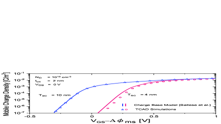
Junctionless (JL) Silicon Nanowire FETs used heavily doped channel to relax several critical fabrication steps and to obviate formation of source/channel and drain/channel junctions, which degrade the performance of short channel devices [1]. To deploy full advantages of Gate-All-Around (GAA) JL devices, several compact model have been proposed so far. Particularly in [2], [3], we developed a charge-based model, using Poisson-Boltzmann equations to model planar and cylindrical junctionless field effect transistors (JLFETs). This model, works for JLFETs with the channel thicknesses down to 10 nm and the device characteristics are well-captured by the proposed model. Nevertheles, this model neglects charge quantization into discrete subband, which is not a valid assumption as channel size decrease below 10 nm. As demonstrated in Fig. 1, the classic charge-based model in [3] fails to predict the charge density in the channel thickness of nm.
To accurately capture the quantization effect, a coupled Poisson-Schrödinger equation (PS) needs to be solved self-consistently.This is a time-consuming calculation method and computationally not suitable for compact modeling purposes. Another work [4] proposed to incorporate the influence of charge quantization as a shift in the DC characteristics. However, due to the coupling between Poisson and Schrödinger equations, this shift varies with the gate to source voltage and therefore this method is not valid in all regions of operation. Lately, taking into account 1D quantum confinement, we developed an analytical approach for ultra-thin junctionless double-gate FETs, which introduces a zero order approximation in the wave-functions and a first order correction for the confined energies in all the regions of operation [5]. In this context, extending the proposed approach we derive an explicit model for junctionless GAA nanowire FET with ultra-thin rectangular cross section.
2 Device structure and Model Derivation
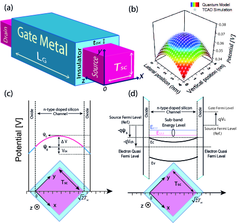
We assume an n-type junctionless nanowire GAA with a rectangular cross section perpendicular to direction, shown in Fig. 2(a) where both the channel thickness (along vertical direction, i.e. ) and the channel width (along lateral direction, i.e. ) are equal to and the gate oxide thickness is all around the silicon channel. The silicon channel is doped uniformly with a high level of donor concentration i.e. and other physical parameters are given in Table I, used in the model derivations and TCAD simulations. The principle of operation for junctionless devices is different from the regular junction-based double-gate device as the current flows through the volume instead of SiSiO2 interfaces [6]. A junctionless nanowire FET transistor has three modes of operation [2]: While the gate to source potential, i.e. , is below the flat-band condition at the source terminal, i.e. device operates in depletion mode. Whereas is above the flat-band condition at the drain terminal, i.e. device is in the accumulation region. A peculiar situation inherent to junctionless FETs is when depletion and accumulation coexist inside the channel, what is called hybrid channel state [2]. This happens when part of the channel near the source is in depletion whereas it turns into accumulation near the drain.
In the following section, applying the proposed treatment in [7] for 2D carrier confinement, the electrostatic potential profiles are accurately predicted in junctionless GAA nanowire FET for to nm silicon thicknesses.
| Parameter | Symbol | Value |
|---|---|---|
| Channel Doping | cm-3 | |
| Channel Thickness | nm | |
| Oxide Thickness | nm | |
| Channel Width | m | |
| Permittivity in Vacuum | F/m | |
| Silicon Permittivity | ||
| Silicon Oxide Permittivity | ||
| longitudinal Effective mass | ||
| Transverse Effective mass | ||
| Silicon Band Gap | eV | |
| Gate Work Function | eV | |
| Conduction Band effective DoS | cm-3 | |
| Valence Band Effective DoS | cm-3 | |
| Silicon Intrinsic Carrier Density | cm-3 | |
| Temperature | K | |
| Mobility | cm-3/V.S | |
| Thermal Voltage | V |
3 Electrostatics in Ultrathin Junctionless GAA nanowire FETs
The 3D electrostatic potential distribution obtained from the TCAD simulation results is shown in Fig. 2(b) for V and nm channel thickness doped at cm-3. Here, we propose to follow the same approach in [8], and to assume a parabolic approximation for the 2D potential distribution in lateral and vertical directions in an ultra-thin junctionless GAA (for both depletion and accumulation regions). Therefore, the parabolic approximation can be expressed as:
| (1) |
as shown in Fig. 2(c) and are respectively the electrostatic potentials at the center and corners of the rectangular channel. In addition, the boundary conditions arising from the continuity of the displacement vectors at the four silicon-insulator interfaces of the square cross section give the total semiconductor charge per unit length: , where is the magnitude of the electric field, obtained from (1). Therefore,
| (2) |
where is directly proportional to . The total charge density is shared among four silicon-insulator capacitors around the channel and an average voltage drop over the gate oxide barrier is defined by where corresponds to the gate oxide capacitance per unit area. On the other hand, varies along the channel interface, leading to
| (3) |
To account for this and to obtain , we integrate (3) around each corner of the rectangle. For instance, once integrating (3) at and from to over -axis and from to over the -axis leads to the following expression for :
| (4) |
By substituting the terms of and obtained from (1) into (4), we get , leading to a key relation between , and :
| (5) |
where corresponds to semiconductor capacitance per unit area. Next, relying on the 1st order perturbation theory, we formulate the charge quantization in discrete sub-bands. Due to two-dimensional (2D) geometrical and electrical confinements in ultra-thin nanowire, mobile charges are confined in discrete sub-bands which are the solutions of the Schrödinger equation in the , plane. An analytical solution can be obtained by assuming an ideal infinite potential well boundary condition at Si-SiO2 interface along with the 1st order perturbation potential inside the channel. For zero order solution, sub-bands energies and wave-functions are given by:
| (6) |
| (7) |
where is the 2D wave function, and is the 2D electrostatic potential in the channel and and are electron effective mass which depends on silicon orientation. In case of orientation, three different series must be considered to properly account for 6 valleys of the effective mass ellipsoid. , and are the longitude and transversal effective mass of electron in silicon, respectively. and are the quantum numbers for and directions that starting from which is the first sub-band. For the first sub-band, due to the degeneracy of 6 valleys in two groups, only two degenerate energy levels exist. The first order correction to the energy eigenvalues is computed using the time-independent perturbation theory:
| (8) |
Replacing obtained from (5) into (1), and the resulting in (8), the integral can be solve analytically and the first order correction of sub-band energies is obtained as a function of , given by
| (9) |
The total energy arising from geometrical and electrical confinements is the summation of (6) and (9), given by
| (10) |
The term of is measured from the reference of the surface electron energy as shown in Fig. 2(d). Total semiconductor charge density per unit length in the nanowire is the sum of fixed charges and mobile charges:
| (11) |
where represents the fix charge density per unit length and is corresponding to the mobile charge density which can be written by using Fermi integral in order of as function of :
| (12) |
where is the distance between the sub-band level and electron quasi-Fermi level in the channel, i.e , the latter varies from at source to at the drain, therefore,
| (13) |
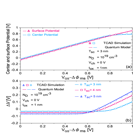
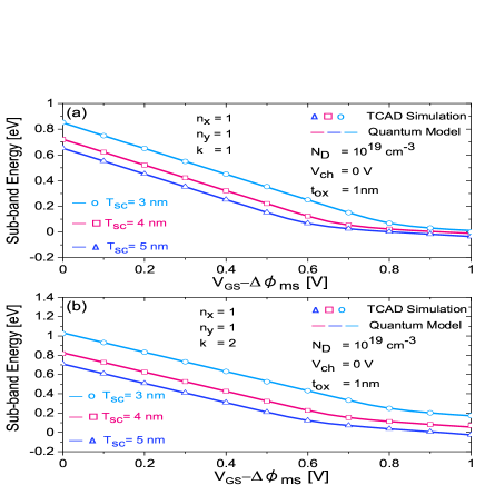
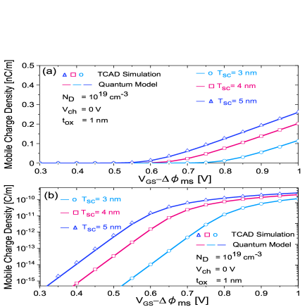
and is one dimensional (1D) effective density of states in nanowire cross section and is the degeneracy factor, for the first sub-band. For a given bias point, (5) and (10) describe the surface potential and sub-band energy, , as a function of . Replacing from (2) and from (12) into (11), a single charge-based equation is solved semi-analytically to obtain the electron energy level, potential profile, and charge density. Fig. 3 shows the surface and center potentials and as a function of . In depletion mode (for small value of ), the mobile charge density is almost negligible, therefore is equal to , and the channel center potential becomes higher than the surface potential, causing an electrical confinement of the carriers wave-function into discrete 2D sub-bands, which enhances the geometrical 2D confinement in the channel. By increasing ( toward the this electrical confinement is relaxed. Fig. 4(a) and 4(b) shows degenerate energy levels for the first sub-band versus for various channel thickness ( nm). This figure clearly shows that the electrical confinement is relaxed by increasing the gate voltage up to the flat-band potential. Fig. 5 represents the mobile charge density versus the effective gate voltage for different channel thicknesses i.e. nm calculated from the proposed model and verified by two-dimensional TCAD simulations results.
4 Derivation of the Drain Current
As in [9], relying on the drift-diffusion transportation model, we propose to calculate the drain current, given by:
| (14) |
where is the free carrier mobility. We intentionally assume a constant mobility to focus on the essentials of electrostatics. Here, and represent the differences between the sub-band and quasi-Fermi levels at the source and drain sides. Replacing (12) into (14), and applying the chain rule for d, we can write:
| (15) |
The term of is obtained from the definition of as:
| (16) |
Replacing from (2) into (5), we can write: , where . Differentiating both sides of this relationship with respect to the we get:
| (17) |
Next, applying the chain rule, is obtained as follows
| (18) |
Using (5) and (10) we can express (18) by
| (19) |
Now we can rewrite (16) based on (17) and (19) as follows
| (20) |
Replacing derivative of with respect to from (12) into (20) we have
| (21) |
where taking into account (19) depends on channel and oxide thickness, therefore is given by
| (22) |
Applying (22) into (15) we can obtain the drain current
| (23) |
Integrating (23) from source to drain we get
| (24) |
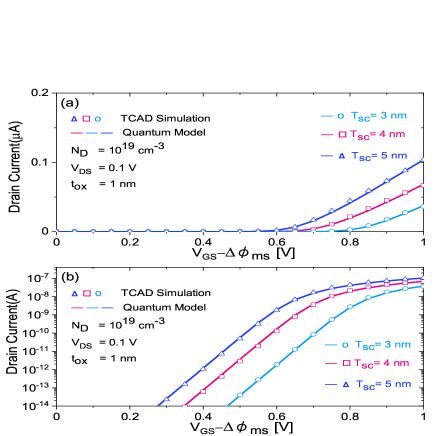
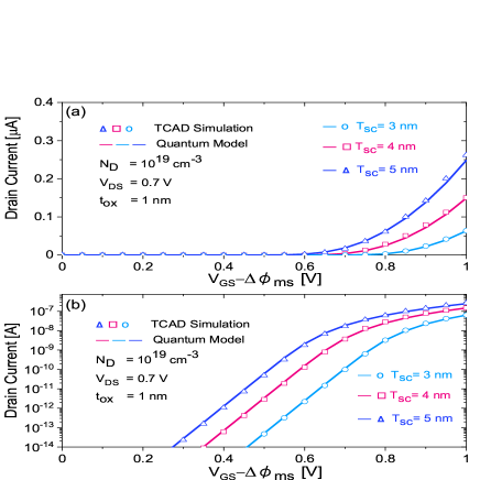
Fig. 6 and Fig. 7 show the drain current versus the effective gate voltage for low ( V) and high ( V) respectively, the length of the channel is m to avoid any short and narrow channel effects. The result predicted by the model shows excellent agreement with TCAD simulations, in both linear and saturation conditions for both charge depletion and accumulation modes. This confirms validation of the model under every operation regions.
Finally, it is worth mentioning that to derive the proposed analytical model, few approximations have been made. First, we assumed infinite quantum well with the first order perturbation theory for sub-band energy estimation and we estimated the potential distribution in channel cross-section by using the parabolic approximation, besides, only the contribution of the first sub-band has been considered in the drain current derivation. These approximations are valid for ultra-thin silicon channel. Nevertheless, as increases above nm, the mobile charge density is distributed non-uniformly near the boundaries of the silicon channel and forms a triangular quantum well, which causes a deviation from the pre-assumed parabolic potential approximation and also affects sub-band energies. Moreover, the contribution of higher sub-bands should not be neglected due to the relaxation of geometrical confinement.
5 Conclusion
In this paper, we derived an analytical model to calculate the two dimensional electrostatic potential distribution in ultra-thin junctionless GAA nanowire FET with channel thickness in the range of to nm. Relying on the drift-diffusion transportation model, we have proposed an analytical model to calculate the drain current in ultra-thin junctionless GAA nanowire FET. The model is valid in all regions of operation, from deep depletion to accumulation and from linear to saturated regimes, as confirmed from a detailed comparison with the TCAD numerical simulations. The proposed model represents an essential step toward dc analysis of circuits/sensors-based on ultra-thin junctionless GAA nanowire FETs. This approach can be further used to derive a full transcapacitances [10, 11] equivalent circuit and short channel effects in ultra-thin junctionless GAA nanowire FETs [12].
References
- [1] Jean-Pierre Colinge, Chi-Woo Lee, Aryan Afzalian, Nima Dehdashti Akhavan, Ran Yan, Isabelle Ferain, Pedram Razavi, Brendan O’Neill, Alan Blake, Mary White, Anne-Marie Kelleher, Brendan McCarthy, and Richard Murphy, “Nanowire Transistors Without Junctions,” Nature Nanotechnology, vol. 5, pp. 225–229, February 2010.
- [2] F. Jazaeri and J.-M. Sallese, Modeling Nanowire and Double-Gate Junctionless Field-Effect Transistors. Cambridge University Press, 2018.
- [3] J. Sallese, N. Chevillon, C. Lallement, B. Iniguez, and F. Pregaldiny, “Charge-based Modeling of Junctionless Double-Gate Field-Effect Transistors,” IEEE Transactions on Electron Devices, vol. 58, no. 8, pp. 2628–2637, Aug 2011.
- [4] J. L. Autran, K. Nehari, and D. Munteanu, “Compact Modeling of the Threshold Voltage in Silicon Nanowire MOSFET including 2D-quantum Confinement Effects,” Molecular Simulation, vol. 31, no. 12, pp. 839–843, 2005.
- [5] M. Shalchian, F. Jazaeri, and J. Sallese, “Charge-Based Model for Ultrathin Junctionless DG FETs, Including Quantum Confinement,” IEEE Transactions on Electron Devices, vol. 65, no. 9, pp. 4009–4014, Sep. 2018.
- [6] F. Jazaeri, N. Makris, A. Saeidi, M. Bucher, and J. Sallese, “Charge-based Model for Junction FETs,” IEEE Transactions on Electron Devices, vol. 65, no. 7, pp. 2694–2698, July 2018.
- [7] T. Numata, S. Uno, J. Hattori, G. Mil’nikov, Y. Kamakura, N. Mori, and K. Nakazato, “A Self-Consistent Compact Model of Ballistic Nanowire MOSFET With Rectangular Cross Section,” IEEE Transactions on Electron Devices, vol. 60, no. 2, pp. 856–862, Feb 2013.
- [8] M. Ferrier, R. Clerc, G. Pananakakis, G. Ghibaudo, F. Boeuf, and T. Skotnicki, “Analytical Compact Model for Quantization in Undoped Double-Gate Metal Oxide Semiconductor Field Effect Transistors and Its Impact on Quasi-Ballistic Current,” Japanese Journal of Applied Physics, vol. 45, no. 4B, pp. 3088–3096, apr 2006.
- [9] E. G. Marin, F. G. Ruiz, V. Schmidt, A. Godoy, H. Riel, and F. Gámiz, “Analytic Drain Current Model for III–V Cylindrical Nanowire Transistors,” Journal of Applied Physics, vol. 118, no. 4, p. 044502, 2015.
- [10] F. Jazaeri, L. Barbut, and J. Sallese, “Trans-capacitance modeling in junctionless symmetric double-gate mosfets,” IEEE Transactions on Electron Devices, vol. 60, no. 12, pp. 4034–4040, Dec 2013.
- [11] F. Jazaeri, L. Barbut, and J.-M. Sallese, “Trans-capacitance modeling in junctionless gate-all-around nanowire fets,” Solid-State Electronics, vol. 96, pp. 34 – 37, 2014. [Online]. Available: http://www.sciencedirect.com/science/article/pii/S0038110114000707
- [12] F. Jazaeri, L. Barbut, A. Koukab, and J.-M. Sallese, “Analytical model for ultra-thin body junctionless symmetric double gate mosfets in subthreshold regime,” Solid-State Electronics, vol. 82, pp. 103 – 110, 2013.