Signatures of free carriers in Raman spectra of cubic In2O3
Abstract
We discuss the influence of free carriers on the Raman scattering in -type In2O3. For high-quality cubic single crystals, electronic single-particle excitations are revealed as a relatively broad Raman feature in the frequency range below 300 cm-1. Furthermore, discrete phonon lines in the same frequency range exhibit asymmetric lineshapes characteristic for Fano resonances. The two observed spectral features contain the potential to be utilized for the quantitative determination of the free carrier concentration in -type In2O3 using Raman spectroscopy as a contactless experimental technique.
Indium oxide, In2O3, is a transparent semiconducting oxide which is widely used as transparent contact material in its heavily Sn doped form. The growing interest in advanced applications, for example in transparent logic elements or conductometric gas sensors, is triggered by the unique properties of crystalline In2O3.(Bierwagen, 2015) For such applications, controlled electrical doping is of crucial importance. Typically, In2O3 exhibits an unintentional -type bulk conductivity in addition to a surface electron accumulation layer and lacks -type conductivity.(Bierwagen, 2015) Regarding the optical characterization of electrical doping in In2O3, infrared absorption spectroscopy and spectroscopic ellipsometry have been successfully utilized.(Fujiwara and Kondo, 2005; Galazka et al., 2014; Feneberg et al., 2016) Raman spectroscopy has been proven as another powerful method to study free carriers in various materials.(Klein, 1975; Abstreiter et al., 1984) The commonly offered microscopic spatial resolution is one benefit of Raman spectroscopy. The possibility to adjust the optical probing depth via the appropriate choice of the excitation wavelength constitutes a further advantage, in particular regarding the investigation of thin films. At the same time, resonance effects can often be exploited to enhance the sensitivity for the detection of Raman signals.(Klein, 1975; Abstreiter et al., 1984) However, the commonly analyzed coupled plasmon-phonon modes cannot be observed in Raman spectra of cubic (bixbyite) In2O3. For centrosymmetric bixbyite crystals only even-parity phonon modes are Raman active (Garcia-Domene et al., 2012; Kranert et al., 2014) for which the formation of coupled plasmon-phonon is not expected.(Klein, 1975; Abstreiter et al., 1984) Instead, spectral Raman features related to single-particle excitations in free carrier gases as well as uncoupled plasmon modes have been reported for different centrosymmetric semiconductors.(Contreras et al., 1985; Cerdeira et al., 1973a, b; Burke et al., 2010; Cerdeira et al., 1984; Wagner and Cardona, 1985; Mortet et al., 2018)
The aim of the present work is to identify the signatures of free carriers in Raman spectra of -type In2O3 having the potential to be utilized for the evaluation of characteristic quantities such as the free electron concentration. Our study on high-quality single crystals reveals a spectral feature due to a continuum of electronic single-particle excitations as well as an accompanying Fano interference with discrete phonon lines.(Fano, 1961)

The investigated cubic bixbyite In2O3 single crystals were grown from the melt by the so-called levitation-assisted self-seeding crystal growth.(Galazka et al., 2013) In order to achieve different doping levels, the crystals were annealed in different atmospheres leading to free electron concentrations (Hall mobilities) in the range of 41017 to 51018 cm-3 (180 to 140 cmVs) as determined by Hall effect measurements.(Galazka et al., 2013, 2014) Raman measurements were performed in backscattering geometry from (111) surfaces of the In2O3 crystals with the sample temperature controlled by a continuous-flow cryostat. The 405-nm (3.06 eV) and 473-nm (2.62 eV) lines of solid-state lasers and the 632.8-nm (1.96 eV) line of a He-Ne laser were used for optical excitation. The incident laser light was focused by a microscope objective onto the sample surfaces. The backscattered light was collected by the same objective without analysis of its polarization, spectrally dispersed by an 80-cm spectrograph (LabRam HR Evolution, Horiba/Jobin Yvon) and detected with a liquid-nitrogen-cooled charge-coupled device (CCD).

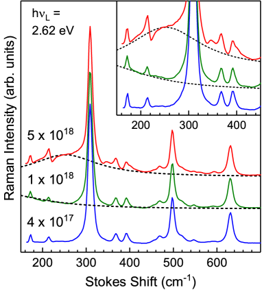
Figure 1 displays room-temperature Raman spectra of In2O3 crystals with different carrier densities for excitation at 2.62 eV. The spectra are dominated by the optical phonon lines at 310, 500 and 630 cm-1. Additional weaker phonon lines are resolved at 170, 215, 370, and 390 cm-1.(Kranert et al., 2014; Garcia-Domene et al., 2012) As expected for centrosymmetric crystals, none of the observed phonon lines exhibits a significant plasmon-coupling induced change in intensity or frequency with increasing doping concentration.(Klein, 1975; Abstreiter et al., 1984) In the case of the highest carrier concentration of 51018 cm-3, however, the low-frequency phonon lines are superimposed on a relatively broad Raman band around 250 cm-1 (dashed line in Fig. 1) and exhibit an asymmetric Fano lineshape.(Fano, 1961) For the sample with the medium carrier concentration of 11018 cm-3, the contribution of a broad Raman feature at low frequencies is still observable (see dashed line). This kind of spectral features have been observed previously in Raman spectra of different degenerately doped semiconductors.(Contreras et al., 1985; Cerdeira et al., 1973a, b; Burke et al., 2010; Cerdeira et al., 1984; Wagner and Cardona, 1985; Mortet et al., 2018; Harima et al., 2000; Mitani et al., 2012) The broad band is commonly attributed to electronic excitations in the conduction band.(Klein, 1975; Abstreiter et al., 1984) The Raman peak of such single-particle intraband excitations generally extends over the frequency range , where is the wavevector transferred during the Raman scattering process and is the Fermi velocity.(Voitenko et al., 1983) For the sample with the highest carrier concentration, is in the range of 100 cm-1 which is clearly below the peak position of the broad band. However, in the case of overdamped excitations, the following relaxation expression is valid to describe the lineshape for electronic intraband Raman scattering:(Contreras et al., 1985; Zawadowski and Cardona, 1990; Ponosov and Streltsov, 2012)
| (1) |
where is the Boltzmann constant, is the sample temperature, and is the electron relaxation rate. The resulting peak position of the Raman band coincides roughly with the value of this relaxation rate. In the case of the most heavily doped sample, 250 cm-1 (see Fig. 1) corresponds to a carrier mobility of 180 cmVs (with the elementary charge and the effective mass ), in reasonable agreement with the measured Hall mobility of 140 cmVs.(Galazka et al., 2013) However, the fitting of the broad Raman band with Eq. 1 does not lead to a satisfactory result. Finally, the lineshape of the broad band could, in principle, be influenced by intersubband transitions between confined states in the surface electron accumulation layer of In2O3.(Nagata et al., 2017, 2019; Abstreiter et al., 1984) This possibility can be ruled out since the occurence of the broad low-frequency Raman band depends strongly on the bulk carrier concentration (cf. Fig. 1). Consequently, further work has to be done to explain more accurately the lineshape of the observed broad Raman band. Once a satisfactory lineshape model is available, the broad low-frequency Raman band could be used for the analysis of free carrier parameters in In2O3.

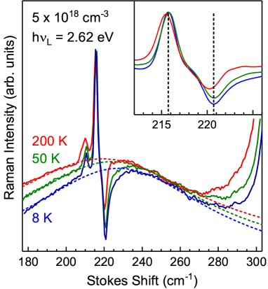
The temperature evolution of the Raman spectra in the low-frequency range is shown in Fig. 2 for the heavily doped sample. With decreasing temperature, the phonon line at 215 cm-1 slightly shifts to higher frequencies (see inset of Fig. 2). Raman features related to electronic excitations are expected to be paricularly temperature dependent, e. g., due to changes in the Fermi distribution function and the carrier mobility.(Voitenko et al., 1983) Indeed, with decreasing temperature the broad low-frequency Raman feature becomes more narrow and shifts to somewhat higher frequencies (see dashed lines in Fig. 2). At the same time, the Fano asymmetry of the phonon line at 215 cm-1 becomes more pronounced. These observations support the assignment of the broad Raman band to electronic single-particle excitations. The Fano-type lineshape for discrete phonon scattering interfering these electronic excitations is given by (Fano, 1961; Wagner and Cardona, 1985)
| (2) |
| (3) |
Here, describes the intensity of electronic scattering without phonon interference, is the frequency of the discrete phonon line in undoped material, is the renormalization shift due to the electron-phonon interaction, and is the phonon linewidth. The electron-phonon matrix element is given by and the Raman efficiency for pure phonon scattering by . The efficiency for Raman scattering by electronic excitations contains information about characteristic free carrier parameters such as the electron concentration.(Cerdeira et al., 1973b) Assuming the broad Raman band to be described by Eq. 1, the spectra in the low-frequency range are given by the superposition .

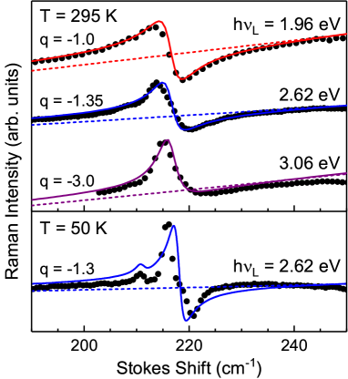
Figure 3 displays low-frequency Raman spectra (symbols) of the most heavily doped In2O3 sample excited at different photon energies. The agreement with simulations obtained by linshape fittings according to Eqs. 2 and 3 (solid lines) confirms the occurence of the Fano-type inferference. For the fitting, the broad Raman band has been taken into account as a linear background signal (see dashed lines in Fig. 3).(Inushima et al., 2003) The lineshapes of the room-temperature spectra can be explained by a constant phonon energy but different asymmetry parameters . Please note, that the line narrowing at low temperatures reveals the contribution of a second weaker phonon line at the low-frequency side (see Fig. 2) leading to a somewhat lower agreement between measured spectrum and fitting curve (see bottom spectrum in Fig. 3).
The asymmetry of the Fano-type lineshape resulting from the interaction between phonon scattering and electronic excitations depends on the relative Raman efficiencies of the underlying scattering mechanisms (see Eq. 3).(Cerdeira et al., 1973b, a) Because of the different resonance behaviors of vibrational and electronic Raman scattering, the asymmetry in the Fano lineshape is, in general, expected to depend on the photon energy used for optical excitation. Indeed, the absolute value of the inverse asymmetry parameter obtained for the room-temperature spectra of the most heavily doped In2O3 sample decreases with increasing photon energy as shown in Fig. 4. Such a monotonic dependence of on the excitation energy has been found, e.g., for heavily doped silicon when approaching resonance conditions with energy gaps at critical points in the electronic band structure.(Cerdeira et al., 1973a; Burke et al., 2010) In the case of -type silicon, a linear increase of has been observed for photon energies in the range between 2.1 and 2.7 eV resulting from the specific resonance behaviors of the involved electronic and vibrational Raman scattering mechanisms.(Cerdeira et al., 1973a) In the present case, the decrease of is attributed to the approaching resonance conditions with the fundamental (2.75 eV) and optical (3.8 eV) band gaps of In2O3.(Feneberg et al., 2016) For a fixed excitation condition, however, the magnitude of the asymmetry parameter , as well as the renormalization shift and the linewidth (see Eqs. 2 and 3) have been demonstrated to be quantitative measures for the carrier concentration in different materials once calibrated by using an appropriate sample series.(Cerdeira et al., 1973b; Harima et al., 2000; Mitani et al., 2012) Furthermore, the lineshape of the Raman peak due to electronic single-particle excitations (see Fig. 1) might contain information about the carrier mobility (see Eq. 1). However, further work is needed to determine the dependence of the lineshape parameters (see Eqs. 1 to 3) on the doping concentration and mobility. Such a calibration has to be done at a fixed excitation energy (see Fig. 4) utilizing a sample series with the carrier concentration varying in a large range.
In conclusion, electronic single-particle excitations and associated Fano interferences with discrete phonon lines are the signatures of free carriers in Raman spectra of -type In2O3. With further calibration work, these spectral features constitute the basis for the evaluation of the free carrier concentration in In2O3 without the need of electrical contacts.
We thank Rüdiger Goldhahn, Martin Feneberg as well as Braulio Garcia Domene for fruitful discussions and Oliver Bierwagen as well as Tobias Schulz for critical reading of our manuscript. This work was performed in the framework of GraFOx, a Leibniz-ScienceCampus partially funded by the Leibniz association. J.F. gratefully acknowledges the financial support by the Leibniz Association.
References
- Bierwagen (2015) O. Bierwagen, Semiconductor Science and Technology 30, 024001 (2015).
- Fujiwara and Kondo (2005) H. Fujiwara and M. Kondo, Phys. Rev. B 71, 075109 (2005).
- Galazka et al. (2014) Z. Galazka, R. Uecker, and R. Fornari, J. Crys. Growth 388, 61 (2014).
- Feneberg et al. (2016) M. Feneberg, J. Nixdorf, C. Lidig, R. Goldhahn, Z. Galazka, O. Bierwagen, and J. S. Speck, Phys. Rev. B 93, 045203 (2016).
- Klein (1975) M. V. Klein, “Electronic Raman Scattering,” in Light Scattering in Solids, edited by M. Cardona (Springer, Berlin, 1975) pp. 147–204.
- Abstreiter et al. (1984) G. Abstreiter, M. Cardona, and A. Pinczuk, “Light scattering by free carrier excitations in semiconductors,” in Light Scattering in Solids IV, edited by M. Cardona and G. Güntherodt (Springer, Berlin, 1984) pp. 5–150.
- Garcia-Domene et al. (2012) B. Garcia-Domene, H. M. Ortiz, O. Gomis, J. A. Sans, F. J. Manjón, A. Muñoz, P. Rodríguez-Hernández, S. N. Achary, D. Errandonea, D. Martínez-García, A. H. Romero, A. Singhal, and A. K. Tyagi, J. Appl. Phys. 112, 123511 (2012).
- Kranert et al. (2014) C. Kranert, R. Schmidt-Grund, and M. Grundmann, Phys. status solidi - Rapid Res. Lett. 8, 554 (2014).
- Contreras et al. (1985) G. Contreras, A. K. Sood, and M. Cardona, Phys. Rev. B 32, 924 (1985).
- Cerdeira et al. (1973a) F. Cerdeira, T. A. Fjeldly, and M. Cardona, Solid State Commun. 13, 325 (1973a).
- Cerdeira et al. (1973b) F. Cerdeira, T. A. Fjeldy, and M. Cardona, Phys. Rev. B 8, 4734 (1973b).
- Burke et al. (2010) B. G. Burke, J. Chan, K. A. Williams, Z. Wu, A. A. Puretzky, and D. B. Geohegan, J. Raman Spectrosc. 41, 1759 (2010).
- Cerdeira et al. (1984) F. Cerdeira, N. Mestres, and M. Cardona, Phys. Rev. B 29, 3737 (1984).
- Wagner and Cardona (1985) J. Wagner and M. Cardona, Phys. Rev. B 32, 8071 (1985).
- Mortet et al. (2018) V. Mortet, A. Taylor, Z. Vlčková Živcová, D. Machon, O. Frank, P. Hubík, D. Tremouilles, and L. Kavan, Diam. Relat. Mater. 88, 163 (2018).
- Fano (1961) U. Fano, Phys. Rev. 124, 1866 (1961).
- Galazka et al. (2013) Z. Galazka, K. Irmscher, M. Pietsch, T. Schulz, R. Uecker, D. Klimm, and R. Fornari, CrystEngComm 15, 2220 (2013).
- Harima et al. (2000) H. Harima, T. Hosoda, and S. Nakashima, in Silicon Carbide and Related Materials - 1999, Materials Science Forum, Vol. 338 (Trans Tech Publications, 2000) pp. 607–610.
- Mitani et al. (2012) T. Mitani, S.-i. Nakashima, K. Kojima, T. Kato, and H. Okumura, J. Appl. Phys. 112, 043514 (2012).
- Voitenko et al. (1983) V. A. Voitenko, I. P. Ipatova, and A. V. Subashiev, JETP Lett. 37, 396 (1983).
- Zawadowski and Cardona (1990) A. Zawadowski and M. Cardona, Phys. Rev. B 42, 10732 (1990).
- Ponosov and Streltsov (2012) Y. S. Ponosov and S. V. Streltsov, Phys. Rev. B 86, 045138 (2012), arXiv:arXiv:1204.4582v3 .
- Nagata et al. (2017) T. Nagata, O. Bierwagen, Z. Galazka, M. Imura, S. Ueda, H. Yoshikawa, Y. Yamashita, and T. Chikyow, Appl. Phys. Express 10, 011102 (2017).
- Nagata et al. (2019) T. Nagata, O. Bierwagen, Z. Galazka, M. Imura, S. Ueda, Y. Yamashita, and T. Chikyow, Jpn. J. Appl. Phys. 58, SDDG06 (2019).
- Inushima et al. (2003) T. Inushima, M. Higashiwaki, and T. Matsui, Phys. Rev. B 68, 235204 (2003).