Two Dimensional Ferromagnetic Semiconductor: Monolayer CrGeS3
Abstract
Recently, two-dimensional ferromagnetic semiconductors have been an important class of materials for many potential applications in spintronic devices. Based on density functional theory, we systematically explore the magnetic and electronic properties of CrGeS3 with the monolayer structures. The comparison of total energy between different magnetic states ensures the ferromagnetic ground state of monolayer CrGeS3. It is also shown that ferromagnetic and semiconducting properties are exhibited in monolayer CrGeS3 with the magnetic moment of 3 for each Cr atom, donated mainly by the intense -hybridization of Cr -S . There are the bandgap of 0.70 eV of spin-up state in the monolayer structure when 0.77 eV in spin-down state. The global gap is 0.34 eV (2.21 eV by using HSE06 functional), which originates from bonding hybridized states of Cr -S and unoccupied Cr -Ge hybridization. Besides, we estimate that the monolayer CrGeS3 possesses the Curie temperature of 161 K by mean-field theory.
I introduction
Graphene with honeycomb structure has been synthesized as extremely thin layers by mechanical exfoliation because of the weak van der Waals out-of-plane interaction, also opens a new field for the two-dimensional crystal with the new physics.1 ; 2 ; 3 ; 4 ; 5 Two-dimensional materials attracted intensive attention partially for their exotic properties. For example, 2D hexagonal boron nitride with a large bandgap of 4.64 eV is reported and possesses enormous potential in electronic and composite applications.6 ; 7 ; 8 ; 9 ; add7 ; add8 And Transition metal dichalcogenides with common structural formula MX2 (M=Mo, W, Ti, etc. And X=S, Se, Te) are found to show electronic properties varying from metals to wide-gap semiconductors with interesting physical characteristics.10 ; 11 ; 12 ; 13 ; 14 MoS2 possesses a transformation from indirect bandgap of bulk to direct bandgap of monolayer, leading to a promising luminescence quantum efficiency.10 Besides, many other compositionally diverse 2D materials have been predicted and in some cases synthesized.15 ; 16 ; 17 ; 18 ; 19
The intrinsic ferromagnetic (FM) semiconductors possess FM and semiconducting properties simultaneously with the fully spin polarization. Compared with diluted magnetic semiconductors, FM semiconductors exhibit tremendous advantages indeed in carrier injection, detection, sensors, magnetic storage and emergent heterostructure devices.add6 However, a few FM semiconductors have been reported up to now limited by the difficult synthesis in experiment. And Mermin-Wagner theory illustrates the absence of intrinsic magnetization with 2D isotropic Heisenberg model at a finite temperature.20 Yet recent studies have shown 2D magnetic crystals can also exhibit magnetism with an Ising model. For example, layer-dependent FM van der Waals crystal like Fe3GeTe2 with an out-of-plane magnetocrystalline anisotropy process a controllable by an ionic gate,add4 and monolayer triiodide chromium (CrI3) is Ising FM material with out-of-plane spin orientation and the of 45 K.add5 Also, nanosheets CrSiTe3 with the indirect bandgap of 0.57 eV have been exfoliated successfully by Lin et al.21 In addition, intrinsic long-range FM order in pristine Cr2Ge2Te6 atomic layers has been reported that the Curie temperature () can be controlled by the very small magnetic fields (smaller than 0.3 T).add3 Furthermore, the feasibility of exfoliation in experiment is confirmed by evaluating the cleavage energy to be very close to graphite.22 of monolayer CrSnTe3 is determined as 170 K, higher than monolayer CrSiTe3 and CrGeTe3. This is attribute to the increased super-exchange coupling between the magnetic Cr atoms by enhanced ionicity of the Sn-Te bond.23
Due to the 2D magnetism in above ABX3-class materials, we use elemental substitution, one of the commonest experimental methods, to improve the physical properties. In this work, we investigate electronic and magnetic structures of monolayer CrGeS3 based on first-principles calculations. The in-plane atoms of CrGeS3 combine with each other by intense covalent bond while the weak van der Waals bonding exists between layers. Additionally, the exfoliation energy is similar to graphene, therefore, we harbor the idea that CrGeS3 can be exfoliated into monolayer successfully. Our results demonstrate monolayer CrGeS3 is dynamically and mechanically stable and possesses intrinsic FM. The electronic structures show that monolayer CrGeS3 is FM semiconductor with global bandgap of 0.34 eV (2.21 eV by HSE06 calculations) and possesses a bandgap of 0.70 eV and 0.77 eV in spin-up and spin-down states, respectively. The magnetic properties result from competition between FM hybridized S holes and AFM itinerant holes in S orbits. Furthermore, electronic exchange interaction and orbital hybridizations in monolayer CrGeS3 crystal lead to the of 161 K in the mean-field theory (MFT). The present results appear promising platform for studying fundamental spin behaviours and promote applications in ultra-compact spintronics.
II computational details
Electronic structure and magnetic properties were carried out using density functional theory (DFT) by the projector augment wave (PAW) method as implemented in the Vienna ab initio simulation package (VASP).24 ; 25 Perdew-Burke-Ernzerhof (PBE) was applied to handle with Exchange-correlation function.26 The accurate global band gap was calculated using the Heyd-Scuseria-Ernzerhof (HSE06) functional including 25% non-local Hartree-Fock exchange.HSE . Cut-off energy for plane wave basis was set up to 450 eV. The number of k points were set as for the monolayer structure. Note that the cutoff energy and the number of k points were all tested assuring that geometry structure gave entire relaxation and sites of atoms reached convergence. The same test was applied in the choice thickness of vacuum slab as 15 Å to separate correlation between adjacent layers. A convergence criterion of for total energy of electronic consistence loop was employed, and 0.01 eV/ Å for Hellmann-Feynman force components in the ions relaxation loop. The partial occupancies were set for each orbital with Gaussian smearing and the width of the smearing was set up to 0.05 eV. A supercell size of primitive unit cells is built to calculated phonon band spectrum by using the density functional perturbation theory (DFPT) Baroni2001 .
III result and discussion
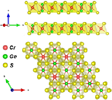
CrGeS3 is a layered material crystallized in space group R (No. 148) and formed by stacks of S-(Ge,Cr)-S sandwich layers with lattice parameters of a=b=6.05 Å. Due to the smaller radius of S atoms than Te atoms, the lattice parameters of plane exhibit a shrinkage compared with a=6.86 Å of CrGeTe3.add2 As shown in fig.1, the monolayer hexagonal honeycomb structure is composed of a Ge2S6 with two Cr ions inserted between two-layers S planes. The monolayer unit cell is composed of two Cr2+ ions and one [Ge2S6]4-. Each Ge atom possesses three neighbouring S atoms forming a tetrahedron and two of Ge-centered tetrahedrons form a dumbbell-like Ge dimer in [Ge2S6]4- bipyramid. The innerlayer atoms are combined by strong covalent bond, while the weak van der Waals interaction exists between layers. Bonds length of Ge-Ge, Cr-S and Ge-S are 2.34 Å, 2.45 Å and 2.23 Å, respectively.
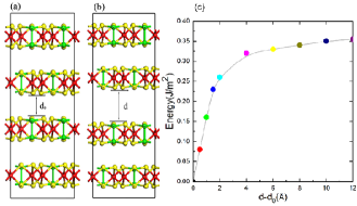
Exfoliation energy is the energy required to cut bulk materials into two halves and is estimated by gradually increasing the distance of two parts (fig.2). The variation of exfoliation energy with the distance [fig.2(c)] reveals that the energy required to break out-of-plane van der Waals binding exhibits an abrupt growing below d=4 Å, while there is a sharp decrease of interaction between two parts. Then the exfoliation energy achieves convergence at an ideal value of 0.35 J/. This value closes to 0.36 J/ in graphene28 and ensures the experimental synthesis of monolayer CrGeS3.
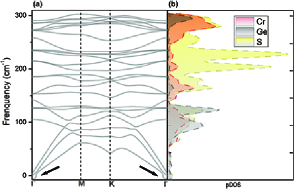
In order to check the dynamic and mechanical stability of the monolayer structure, we calculate phonon spectrum and projected density of states of phonon, as shown in fig.3. Two negligible small pockets of instability occur near point labelled as black arrow [fig.3(a)]. The pockets are extremely sensitive to computational details. Also, there is the altogether absence of these imaginary frequency in some cases with respect to our calculations. Note that it is difficult to achieve numerical convergence for the flexural phonon branch, which is considered as a common issue in first-principles calculations for two-dimensional materials.pho1 ; pho2 ; pho3 ; pho4 Therefore, the phonon spectrum suggests that monolayer CrGeS3 is dynamically stable.
The energetic stability of monolayer CrGeS3 can be evaluated by formation energy Ef as
| (1) |
where is the corresponding normalized energy for different structures. The negative of -0.61 eV indicates monolayer CrGeS3 is energetically stable. For a further detecting mechanical stability, we also calculate the elastic constants and of monolayer CrGeS3. The two independent parameters are given as,
| (2) |
where is total energy of an unit cell and is the equilibrium area of monolayer CrGeS3. The calculated and are 64 N/m and 17 N/m, respectively. It is evident that our results satisfy the Born criterion of stability ()29 .
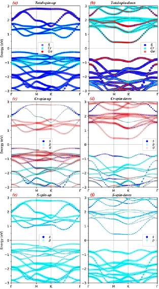
For exploring into the electronic properties of monolayer CrGeS3, we plot the spin polarized band structure diagrams as shown in fig.4. The spin-down components exhibit similar mechanism of electronic interaction of conduction bands and valence bands with spin-up state, so the spin-up components are discussed here mainly [fig.4(a), (c) and (e)]. The spin-up band structure possesses the bandgap of 0.70 eV. The conduction band originates from significant hybridization between empty antibonding bands of Cr -S orbits at 1 eV above the Fermi level when valence band is the fully occupied -hybridized bonding states of Cr -S at about -0.5 eV under the Fermi level. The highly localized antibonding bands of Cr atoms are mainly composed of unoccupied, polarized orbits. In comparison, an effective exchange interaction of the bonding-states Cr atoms is generated by the - hybridization. Additionally, the occupied Ge -S hybridization in spin-down channel [fig.4(b), (d) and (f)] results from the tetrahedral-coordinated Ge atom surrounded by three S atoms in [Ge2S6]4-, so the Ge hybrid orbits lead to bonding states of Ge -S .
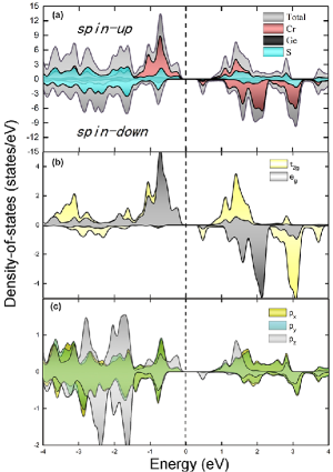
To help a further understanding of the electronic structure of monolayer CrGeS3, we present the project density of states based on PBE functional as shown in fig.5. Figure 5 (a) ensures the global bandgap of 0.34 eV and a more accurate value is investigated as 2.21 eV based on HSE06 functional. The CrGeS3 crystal field splits the orbits of Cr atoms into upper (, ) and lower (, , ) states, as shown in fig.5(b). The prominent feature of the electronic structure is the fully occupied Cr bands at about -0.5 eV under the Fermi level and the empty spin-down orbits of Cr atoms localizing at about 2.1 eV above the Fermi level, indicating a spin split (about 0.42 eV) between the localized Cr states. The bonding hybridized states of Cr -S and the unoccupied Cr -Ge hybridization results in valence band maximum and conduction band minimum. Apart from this, each orbits of Cr atom hybridizes significantly with S states, forming a bonging and antibonding pair bonds of Cr -S . But the weaker bonding gives rise to the localized Cr states, which is agreed with former research on ABX3 type transition metal tri-chalcogenides.add1
Now we estimate the magnetic properties by comparing FM and AFM phase of monolayer CrGeS3. The results show the AFM state possesses a higher energy about 50 meV than FM state. The FM coupling is contributed by the hybridized holes of S atoms. And the holes are originated from strong -hybridization between Cr and orbits of S atoms. Apart from the regular super-exchange interactions mentioned above, the itinerant holes in orbits of S atoms can also be coupled with the neighboring Cr spins antiferromagnetically, leading to a mediation of FM-states moments of Cr atoms. Thus, the local magnetic moment of one Cr atom is 3.27 with an extra 0.27 originating from the bonding states of Cr -S . Actually, this interaction of Cr orbits and S leads to the S holes with an opposite spin polarization of -0.11 each S atom according to our results. Then the magnetic moment of a Cr atom remains 3 .
For magnetic materials, Curie temperature is a crucial parameter determining a temperature at which intrinsic magnetic intensity decrease to 0 and FM phase transforms into nonmagnetic phase.30 ; 32 ; 33 We main focus on predicting in accordance with MFT34 as
| (3) |
where is the number of nearest-neighboring Cr atoms of a Cr atom in monolayer CrGeS3, is the exchange integral, is the spin of each Cr atom, and is the Boltzmann constant. The value of is consistent with the magnetic moment of 3 for each Cr atom. We induce another term as exchange energy between the two Cr atoms in unit cell, defined as
| (4) |
The total energies of monolayer CrGeS3 primitive cell with the FM and AFM configurations and can be calculated as well.35 Accordingly, the difference between and gives . As a result, we can obtain the exchange integral with the PBE functional as 1.85 meV. We further obtain of 161 K in monolayer CrGeS3. For comparison, the of CrGeTe3 with a similar structure via Monte Carlo (MC) simulation is 61 K36 . Note that the MFT generally overestimates the 37 compared with MC simulations and we just provide a prediction of monolayer CrGeS3. The properties suggest that monolayer CrGeS3 have potential applications in spin-polarized carrier injection, detection, ultra-compact spintronics, and also support a platform for studying electronic mechanism in 2D materials.22
IV Conclusion
In summary, we have investigated the stability, electronic and magnetic properties of monolayer CrGeS3 based on first-principles calculations. It is found that monolayer CrGeS3 is dynamically and mechanically stable and could be successfully synthesized due to the similar exfoliation energy to graphene. After that, honeycomb structural monolayer CrGeS3 exhibits FM ground state with magnetic moment of 3 per Cr atoms. The reason of this magnetism is the competition between bonding states of Cr -S intercoupling ferromagnetically and opposite spin polarization from S holes. The indirect bandgaps are 0.34 eV (2.21 eV based on HSE06 functional), 0.70 eV and 0.77 eV in global, spin-up and spin-down states respectively, which result from the interaction between bonding hybridized states of Cr -S and unoccupied bonds of Cr -Ge . In addition, we roughly estimate the of magnetic transition as 161 K by MFT. Our results illustrate that monolayer CrGeS3 crystals will possess enormous applications in nanoscale spintronics. We also expect our theoretical study will inspire further experimental studies.
Acknowledgements.
This work was supported by the NSFC (Grants No.11874273), the Specialized Research Fund for the Doctoral Program of Higher Education of China (Grant No.2018M631760), the Project of Heibei Educational Department, China (No.ZD2018015), the Advanced Postdoctoral Programs of Hebei Province (No.B2017003004).References
- (1) K. S. Novoselov, A. K. Geim, S. V. Morozov, D. Jiang, Y. Zhang, S. V. Dubonos, I. V. Grigorieva and A. Firsov, Science 306, 666-669 (2004).
- (2) Q. H. Wang, K. Kalantar-Zadeh, A. Kis, J. N. Coleman and M. S. Strano, Nat. Nanotechnol. 7, 699 (2012).
- (3) A. K. Geim and I. V. Grigorieva, Nature 499, 419 (2013).
- (4) V. Nicolosi, M. Chhowalla, M. G. Kanatzidis, M. Strano and J. N. Coleman, Science 340, 1226419 (2013).
- (5) T. J. Williams, A. A. Aczel, M. D. Lumsden, S. E. Nagler, M. B. Stone, J. Q. Yan, and D. Mandrus, Phys. Rev. B 92, 144404 (2015).
- (6) G. Cassabois, P. Valvin and B. Gil, Nat. Photonics 10, 262 (2016).
- (7) W. Gannett, W. Regan, K. Watanabe, T. Taniguchi, M. F. Crommie and A. Zettl, Appl. Phys. Lett. 98, 242105 (2011).
- (8) K. K. Kim, A. Hsu, X. Jia, S. M. Kim, Y. Shi, M. Dresselhaus, T. Palacios and J. Kong, ACS Nano 6, 8583-8590 (2012).
- (9) K. Watanabe and T. Taniguchi, Int. J. Appl. Ceram. Technol. 8, 977-989 (2011).
- (10) M. Topsakal, E. Aktürk, and S. Ciraci, Phys. Rev. B 79 115442 (2009).
- (11) D. Pacile, J. C. Meyer, C. ö. Girit, and A. Zettl, Appl. Phys. Lett. 92 133107 (2008).
- (12) K. F. Mak, C. Lee, J. Hone, J. Shan and T. F. Heinz, Phys. Rev. Lett. 105, 136805 (2010).
- (13) D. J. Late, B. Liu, H. S. S. R. Matte, C. N. R. Rao and V. P. Dravid, Adv. Funct. Mater. 22, 1894-1905 (2012).
- (14) G. Eda, H. Yamaguchi, D. Voiry, T. Fujita, M. Chen and M. Chhowalla, Nano Lett. 11, 5111-5116 (2011).
- (15) C. H. Lui, A. J. Frenzel, D. V. Pilon, Y. H. Lee, X. Ling, G. M. Akselrod, J. Kong, and N. Gedik, Phys. Rev. Lett. 113, 166801 (2014).
- (16) A. H. Reshak, I. V. Kityk and S. Auluck, J. Chem. Phys. 129, 074706 (2008).
- (17) S. Lebgue and O. Eriksson, Phys. Rev. B 79, 115409 (2009).
- (18) M. Ashton, J. Paul, S. B. Sinnott, and R. G. Hennig, Phys. Rev. Lett. 118, 106101 (2017).
- (19) L. Zhou, L. Kou, Y.Sun, C. Felser, F. Hu, G. Shan, S. C. Smith, B. Yan and T. Frauenheim, Nano Lett. 15, 7867-7872 (2015).
- (20) L. Debbichi, H. Kim, T. Björkman, O. Eriksson, and S. Lebgue, Phys. Rev. B 93, 245307 (2016).
- (21) H. Liu, A. T. Neal, Z. Zhu, Z. Luo, X. Xu, D. Tomnek and P. D. Ye, ACS Nano 8, 4033-4041 (2014).
- (22) C. Gong and X. Zhang, Science 363, 706 (2019).
- (23) N. D. Mermin and H. Wagner, Phys. Rev. Lett. 17, 1133 (1966).
- (24) M. W. Lin, H. L. Zhuang, J. Yan, T. Z. Ward, A. A. Puretzky, C. M. Rouleau, Z. Gai, L. Liang, V. Meunier, B. G. Sumpter, P. Ganesh, P. R. C. Kent, D. B. Geohegan, D. G. Mandrusbc and K. Xiao, J. Mater. Chem. C 4, 315-322 (2016).
- (25) C. Gong, L. Li, Z. Li, H. Ji, A. Stern, Y. Xia, T. Cao, W. Bao, C. Wang, Y. Wang, Z.Q. Qiu, R.J. Cava, S.G. Louie, J. Xia, and X. Zhang, Nature 546, 265 (2017).
- (26) X. Lia and J. Yang, J. Mater. Chem. C 2, 7071-7076 (2014).
- (27) H. L. Zhuang, Y. Xie, P. R. C. Kent, and P. Ganesh, Phys. Rev. B 92, 035407 (2015).
- (28) Y. Deng, Y. Yu, Y. Song, J. Zhang, N. Z. Wang, Z. Sun, Y. Yi, Y. Z. Wu, S. Wu, J. Zhu, J. Wang, X. H. Chen, and Y. Zhang, Nature 563, 94-99 (2018).
- (29) B. Huang, G. Clark, E. Navarro-Moratalla, D.R. Klein, R. Cheng, K.L. Seyler, D. Zhong, E. Schmidgall, M.A. McGuire, D. H. Cobden, W. Yao, D. Xiao, P. Jarillo-Herrero, and X. Xu, Nature 546, 270 (2017).
- (30) P. E. Blöchl, Phys. Rev. B 50, 17953 (1994).
- (31) G. Kresse and J. Furthmüller, Phys. Rev. B 54, 11169 (1996).
- (32) M. Ernzerhof and G. E. Scuseria. J. Chem. Phys. 110, 5029-5036 (1999).
- (33) J. Heyd, G. E. Scuseria, M. Ernzerhof, J. Chem. Phys. 118, 8207-8215 (2003).
- (34) S. Baroni, S. D. Gironcoli, A. D. Corso, and P. Giannozzi, Rev. Mod. Phys. 73, 515 (2001).
- (35) K. Wang, T. Hu, F. Jia, G. Zhao, Y. Liu, I. Solovyev, A. P. Pyatakov, A. K. Zvezdin, and W. Ren, Appl. Phys. Lett. 114, 092405 (2019).
- (36) R. Zacharia, H. Ulbricht and T. Hertel, Phys. Rev. B 69, 155406 (2004).
- (37) L. F. Huang, and Z. Zeng, J. Appl. Phys. 113, 083524 (2013).
- (38) L. F. Huang, P. L. Gong, and Z. Zeng, Phys. Rev. B 90, 045409 (2014).
- (39) L. Huang, P. Gong, and Z. Zeng, Phys. Rev. B 91, 205433 (2015).
- (40) N. Mounet, and N. Marzari, Phys. Rev. B 71, 205214 (2005).
- (41) H. L. Zhuang, M. D. Johannes, M. N. Blonsky, and R. G. Hennig, Appl. Phys. Lett. 104, 022116 (2014).
- (42) S. Kang, S. Kang, and J. Yu, J. Electron. Mater. 114, 092405 (2018).
- (43) Y. Li and K, Baberschke, Phys. Rev. L 68, 1208 (1992).
- (44) A. Du and G. Z. Wei, Aust. J. Phys. 46, 571-582 (1993).
- (45) L. Capriotti, R. Vaia, A. Cuccoli and V. Tognetti, Phys. Rev. B 58, 273 (1998).
- (46) B. D. Cullity and C. D. Graham, Introduction to magnetic materials, John Wiley and Sons, (2011).
- (47) J. Zhou and Q. Sun, J. Am. Chem. Soc. 133, 15113-15119 (2011).
- (48) B. Siberchicot, S. Jobic, V. Carteaux, P. Gressier, and G. Ouvrard, J. Chem. Phys. 100, 5863-5867 (1996).
- (49) M. Kan, S. Adhikarib and Q. Sun, Chem. Phys. 16, 4990-4994 (2014).