Bias induced circular spin current: Effects of environmental dephasing and disorder
Abstract
Analogous to circular spin current in an isolated quantum loop, bias induced spin circular current can also be generated under certain physical conditions in a nanojunction having single and/or multiple loop geometries which we propose first time, to the best of our concern, considering a magnetic quantum system. The key aspect of our work is the development of a suitable theory for defining and analyzing circular spin current in presence of environmental dephasing and impurities. Unlike transport current in a conducting junction, circular current may enhance significantly in presence of disorder and phase randomizing processes. Our analysis provides a new spin dependent phenomenon, and can give important signatures in designing suitable spintronic devices as well as selective spin regulations.
I Introduction
The phenomenon of bias induced circular charge current in a conducting nano junction having single or multiple loop geometries has been a new paradigm of research over last few years cir1 ; cir2 ; cir3 ; cir4 ; cir5 ; cir6 ; cir7 ; cir8 ; cir9 ; cir10 . We are mostly familiar with transport current, which is usually referred as junction current, through a source-conductor-drain bridge system. But, when the bridging conductor contains a loop structure, a net circular current may be generated due to voltage bias satisfying some conditions cir1 ; cir2 ; cir3 ; cir4 ; cir5 ; cir6 ; cir7 ; cir8 ; cir9 ; cir10 . This is quite analogous to the appearance of circular current (more usually known as persistent current) in an isolated mesoscopic ring-like structure (not connected with external baths) upon the application of magnetic field pc1 ; pc2 ; pc3 ; pc4 ; pc5 . Though the phenomena are quite similar, the origins of these two currents are completely different. In one case it is due to external magnetic field and in the other case voltage bias is responsible. We will focus on the latter one in our present work.
The study of bond currents in different arms cir1 ; cir2 ; cir3 ; cir4 ; cir5 ; bond1 ; bond2 of a connected ring-like geometry essentially triggers that a circular current can be possible if the electrodes are attached properly such that the contributions from different arms do not mutually cancel with each other. Naturally, a possibility of tuning such current can be imagined by changing the junction configuration. Now what makes this phenomenon so special is that, this circular current induces a very large magnetic field cir5 ; cir6 ; cir7 ; cir8 ; cir9 at its center as well as away (not so far) from the center. Because of smaller ring size, strong magnetic field, in some cases it may even reach to few millitesla or even tesla, will be induced, that can be served in many ways. The most probable application may be the proper regulation of electron spin or local magnetic moment, which can be utilized to perform different operations like storage of data, logic functions, spin switching, spin selective electron transmission, spin based quantum computations, to name a few app1 ; app2 ; app3 ; app4 ; app5 ; app6 ; app7 .
Thus, whenever we think about the tuning of a single spin or a magnetic moment, the application of a ‘local magnetic field’ may be a worthy option for it. Few proposals have already been made lm1 ; lm2 for generating and controlling of magnetic field locally, among them circular current induced magnetic field cir5 ; cir6 ; cir7 ; cir8 ; cir9 will be the most suitable one, as on one hand it is very large and on the other hand its tuning is relatively simple rather than other propositions. So far, the phenomenon of ‘charge circular current’ in nanojuctions has been studied cir1 ; cir2 ; cir3 ; cir4 ; cir5 ; cir6 ; cir7 ; cir8 ; cir9 ; cir10 , and no one has explored spin dependent circular current, to the best of our knowledge, which might bring several salient features along this line, and thus probing into it is undoubtedly very essential.
In the present communication we do an in-depth analysis of circular spin current in a nanojuction considering a magnetic quantum ring within a tight-binding (TB) framework. To make the
model more realistic we include the effects of disorder and environmental dephasing. The main attention is given in developing a suitable theory for describing circular spin current density, and thus circular current, in presence of dephasing. We introduce dephasing effect by connecting Büttiker probes dp1 ; dp2 ; dp3 ; dp4 ; dp5 at each lattice sites of the bridging conductor, and it can be assumed as the most convincing and appropriate way to include phase randomization processes in transport phenomena. Instead of Büttiker probes, adding a constant damping factor one can also introduce dephasing into the system, as already reported in few works cir5 ; damp1 ; damp2 , but in this mechanism all the essential features may not be captured. The Büttiker probes alter the conservation conditions of different bond currents that should be incorporated properly to define the current densities.
Thus, the emphasis will be given in two aspects: (i) establishing a proper methodology for calculating circular current in presence of dephasing via Büttiker probes, and (ii) defining bias induced spin circular current. These aspects have not been addressed earlier. We strongly believe that the characteristic features emerged from our analysis may provide some valuable inputs that can be exploited to investigate several spin dependent phenomena.
The arrangement of the remaining part of this paper is as follows. In Sec. II, we describe different spin-dependent conserved quantities and finite relations among them. In Sec. III, we illustrate the complete theoretical prescription for analyzing the phenomenon of bias induced circular spin current in presence of spin dependent scattering mechanism. In Sec. IV, we examine the accuracy of our theoretical prescription based on which the results are computed. This will give us a confidence of our theoretical prescription. All the essential results are throughly discussed in Sec. V, and finally, we summarize our findings in Sec. VI.
II General definition of circular current and different spin-dependent conserved quantities
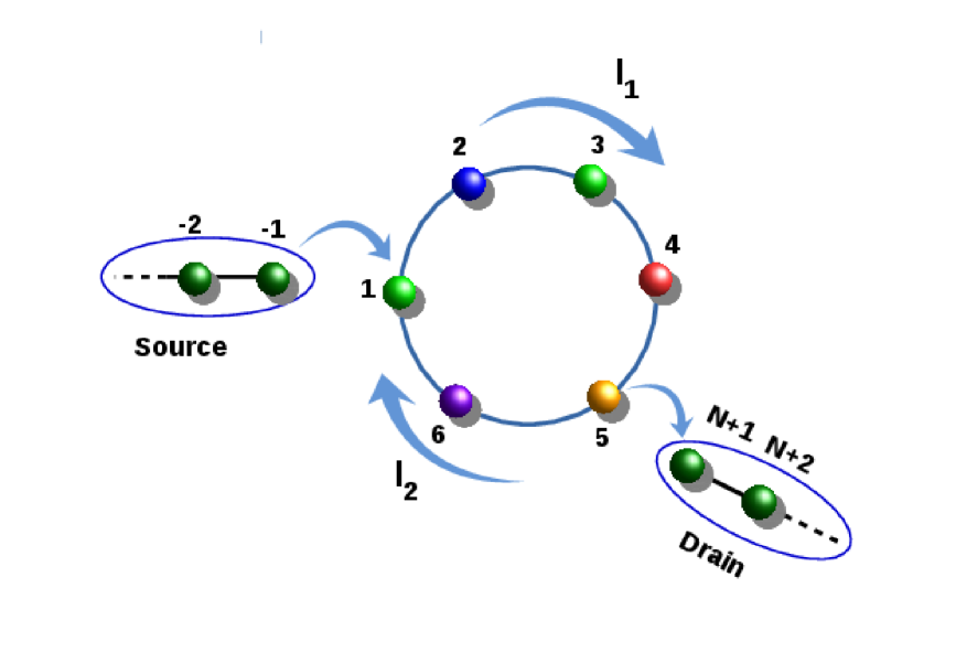
To define circular current, let us start with Fig. 1, where a net current flows from source to drain through the conducting ring. The current, which enters into the ring divided into two parts, (say) and , and they re-unite at the drain end. We assign positive sign
to the current propagating in the clockwise direction. If and be the number of atomic sites in the upper and lower arms of the ring, respectively, then we define circular current in the ring as cir5 ; cir9
| (1) |
where, is the inter-atomic spacing. Now, for a symmetrically connected junction where , the currents in the upper and lower arms are identical in magnitude and opposite in sign, which results a vanishing circular current. Thus, in order to have a net circular current, we need to break the status between the upper and lower arms of the ring cir5 ; cir9 . It can be done in many ways: either by considering unequal lengths of a perfect junction or by introducing impurities in different arms of a lengthwise symmetric junction or by both.
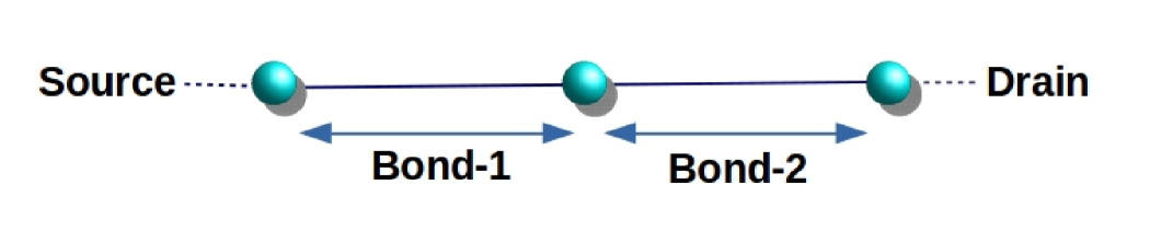
For the calculation of currents in different sectors, first we have to properly define the bond currents, and it is always easy to start with a simple linear geometry (for instance see Fig. 2). In this chain-like geometry, the bond current between any two adjacent sites and () can be expressed as green1 ; green2
| (2) |
where, is the bond current density. This expression is equally valid for any geometry, be it a chain or any other shaped conductor. Now, when we stick to the liner chain model, the bond current should be exactly identical to that of the transport current cir6 ; damp2 , defined as green1
| (3) |
where, is the transmission function. From Eqs. 2 and 3, we get the condition (setting ). The factor appears due to spin degeneracy. This is the fundamental relation to define bond current density in a linear geometry cir6 ; damp2 , and we will extend it accordingly to calculate currents in different segments of any geometrical shaped conductor of our interest.
The scenario becomes more tricky and interesting as well when we consider spin degree of freedom. Under this situation, the above relation becomes where . Depending on pure spin transmission and spin flip transmission, we will have different spin dependent bond currents. Below we summarize the properties of spin dependent bond current densities and their conservation conditions (following the same physics as used for the spin-less case cir6 ; damp2 ) considering a simple set up shown in Fig. 2 and that can be easily generalized for other complicated junctions as well.
Case I - In absence of spin flip transmission:
-
a.
When spin flip transmission is absent, the relations between different spin dependent current densities with transmission components are as follows. ; , and . Thus, as an example, we can write these relations for Fig. 2 as: and . And, the spin flipped terms are: . Here, all the spin dependent current densities in different bonds are conserved.
Case II - In presence of spin flip transmission:
-
a.
In presence of spin flip transmission, different components behave as follows. ; ; ; . Thus, for the two bonds shown in Fig. 2 we get ; ; ; and . Here individual components are no longer conserved for different bonds.
-
b.
Another interesting observation is that for a particular bond becomes identical with in that specific bond, but they vary from bond to bond i.e., is no longer identical with .
-
c.
When we combine spin flip transmissions along with pure spin transmission, we get conserved quantities for each distinct bonds. They are are prescribed as follows. Total up spin current density . Similarly, for down spin electrons, the current density . So, for the bonds and we get the relations for up spin electrons, and, for down spin electrons the conditions are .
Here we would like to note that in the above expressions, the first term in the subscripts of and is used for the incident spin, while the second one for the transmitting electron. All these relations are equally valid even in the presence of disorder and environmental dephasing.
III Theoretical Formulation of circular spin current
Our ultimate goal is to develop a suitable theory for defining spin dependent circular current in a nanojunction having a loop geometry in presence of impurities and environmental dephasing. To do that we proceed in three steps. First, we try to formulate the (effective) bond current density in presence of dephasing for the spin less case considering a linear geometry (described in Sec. IIIA), which is always easy to understand. Second, we extend the idea for the same system considering spin degree of freedom (available in Sec. IIIB). Finally, we apply the idea into a ring-like geometry to have spin current density and thus spin circular current (discussed in Sec. IIIC).
From the conservation relations analyzed above it is clear that the bond current densities are directly linked to the transmission functions. Thus, to get bond currents, we need to find transmission co-efficients. Several methods are there like wave-guide theory wg1 ; wg2 ; wg3 ; wg4 , transfer-matrix method app6 ; tm1 ; tm2 and Green’s function approach green1 ; green2 ; new5 through which transmission probability can be calculated, and in the present work, we opt the wave-guide theory based on nearest-neighbor TB model.
A. Formulation of current density in a 1D chain in presence of dephasing for the spin less case: Let us start with Fig. 3 where a 1D non-magnetic (NM) chain (it can also be called as channel) is coupled to source (S) and drain (D) electrodes along with the Büttiker probes. All these electrodes are assumed to be perfect, NM and semi-infinite. The Hamiltonian for the entire system becomes
| (4) |
where , , , and represent the Hamiltonians for the channel (C), S, D, and the Büttiker probes (B), respectively. The general form of TB Hamiltonian for these sub-systems in nearest-neighbor hopping (NNH) approximation looks like
| (5) |
where, =C, S, D, and B. For all the electrodes, we refer and it is for the channel C. In the absence of any voltage bias, we call for the electrodes, while for the channel C, it becomes ( be the site index). These site energies get modified as long as the bias is included, and the dependence of these energies on bias can be clearly understood from our forthcoming analysis. The last term, , of Eq. 4 describes the tunneling Hamiltonian due to the coupling of the channel with S, D, and dephasing leads, and it is also expressed in the usual TB form.
To calculate transmission probability and circular current density, we solve a set of coupled linear equations originated from the time-independent Schrödinger equation , where represents the wave-function and is the identity matrix. Now, for the multi-terminal set up, shown in Fig. 3, we need to consider three different cases taking separately any one among the source, dephasing lead-1 and lead-2 as the incoming lead, while the other two including the drain as the outgoing leads. First, we consider S as the input lead, and thus, transmitting electrons will be collected by all the other leads. In this case the coupled equations for the perfect conductor look like damp2 ; wg3 :
Here we assume that, a plane wave with unit amplitude is injected from the source end. The parameters , and represent the coupling between S-to-C, C-to-D, and channel-to-dephasing lead, respectively. The symbols and correspond to the reflection and transmission amplitudes, respectively. The meaning of different equations and the appearance of some other factors like , , along with the wave-vectors (viz, , , etc.) can be understood explicitly as follows. To get bias induced circular current we need to apply a finite bias across the conductor, and at the same time we have to impose the condition that the net current through each dephasing electrode (Büttiker probe) is zero. To have this zero current condition for the dephasing electrodes, the voltages (say) (in th electrode) should be adjusted accordingly. These voltages () can easily be derived from the Landauer-Büttiker current expression green1 ; green2 of each virtual
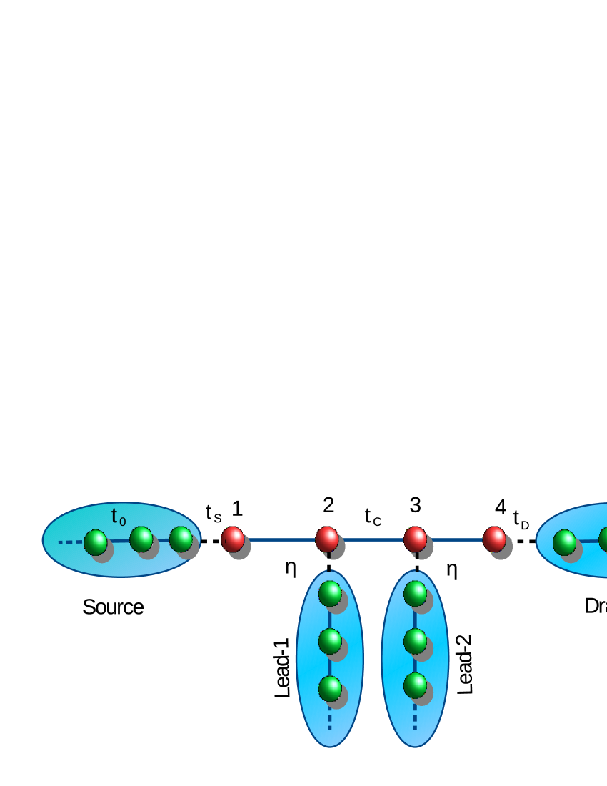
lead, and noting the voltage drop at different lattice sites. Suppose, a bias is applied between the real electrodes i.e., and ( and are the voltages associated with S and D). Then for the four-site chain geometry shown in Fig. 3, the voltage at site 1, where S is connected, will be and it will be zero at site 4, where D is attached. Assuming identical voltage drop, as the voltage difference () is shared into three bonds (for 4-site chain), we can find the voltages at different lattice sites of the chain. Thus at site 1, the voltage becomes , and for the sites 2, 3 and 4 the voltages are , and 0, respectively. Setting the bias voltage in this fashion (viz, , ) across the virtual electrodes, we can impose the zero current condition. This prescription can easily be generalized for any -site chain as clearly demonstrated earlier by several groups dp3 ; dp4 ; dp5 ; green1 ; green2 ; dp6 ; niko . In presence of non-zero bias between S and D as the electrochemical potentials of different electrodes (real and virtual) are different new1 , the site energies of the electrodes get shifted by constant factors associated with the voltages, and accordingly, the wave-vectors , , and are modified. The site energies of the bridging conductor (viz, channel C) get modified following the bias drop along the chain. All these factors are incorporated properly in different site equations of Eq. LABEL:eq3, and they are now voltage dependent (for comprehensive analysis see Refs. new2 ; new3 ; new4 ).
Solving the set of coupled equations given in Eq. LABEL:eq3, we get the voltage dependent transmission probability at different electronic energies at the drain electrode i.e., and the bond current density between the sites and of the channel. These are respectively expressed as
| (7) |
and
| (8) | |||||
The term in the denominator of Eq. 8 corresponds to the incident current density cir5 ; damp2 . The subscript in the above current density expression is used to denote that Eq. 8 is derived when the source (S) acts as the input lead. For the other input leads we replace by appropriate symbols as can be understood from our forthcoming formulation.
Now we move to the other case, where the lead-1 (Büttiker probe) acts as the input lead. For this case the coupled equations are expressed as given in Appendix A, and solving Eq. LABEL:eq6 we compute and , like what we do in Eqs. 7 and 8.
Similarly, considering the other Büttiker probe (viz, lead-2) as an input lead we evaluate and solving the set of coupled equations (Eq. 18) as described in Appendix A.
Following these mathematical steps we calculate the transmission probabilities and current densities at different segments for three different input conditions. We ultimately want to find an effective expression of current density for the full system with the help of current densities of different regions in the presence of dephasing.
Under the condition that the current through each Büttiker probe is zero, we can express the net transmission probability for the set up given in Fig. 3 as dp3 ; dp4 ; dp5 ; dp6
| (9) | |||||
where the ratio is determined from the above analysis. For a -site conductor this expression will be extended accordingly.
Now, in presence of the Büttiker probes we define the current density in any arbitrary bond connecting the sites and () as
| (10) |
From the current conservation conditions, we will have the following relations between the transmission probabilities and current densities of different bonds of the junction configuration given in Fig. 3.
| (11) |
It is well known that for a strictly 1D chain should always be identical with cir5 ; damp2 (where the factor comes due to spin degeneracy). Thus, combining Eqs. 9 and 11, we get the effective expression of in presence of dephasing in the form
| (12) | |||||
which is utilized to find the current density in a 4-site chain as prescribed in Fig. 3.
The above expression of can routinely be extended for any arbitrary 1D chain having lattice sites where the dephasing leads are connected at all the sites except the boundary ones (like what is shown in Fig. 3), and it reads as
| (13) |
B. Formulation of current density in a 1D chain in presence of dephasing considering spin degree of freedom: Now we consider the spin degree of freedom to generalize the above prescription for the same set up as taken in Fig. 3. Similar to the spin less case, here also we will have three different cases based on the choices of the leads among the source and two dephasing leads as the input one. For each input lead, we have two distinct cases depending on which spin (up and down) of electron gets injected wg4 .
First we consider the source S as the input lead. We modify Eq. LABEL:eq3 in the spin basis to have the required sets (both for up and down spin incidences) of coupled equations, as prescribed in Appendix B.
In the same footing, we consider the dephasing leads one by one as the input terminal, and modify Eqs. LABEL:eq6 and 18, accordingly, in the spin basis. Solving these sets of equations we get all the required coefficients to evaluate the spin dependent current densities at different segments. Finally, we define the net up and down spin current densities as and , respectively, where is evaluated following the similar kind of steps given in Eqs. 8, 10, and 12. The expressions can be generalized further for any -site system following the mechanism given in Eq. 13. Using and we define the net charge and spin current densities as: and , respectively.
C. Circular current in a 1D ring: Utilizing the above concept, we can now determine the current density and circular current in a nanojunction having a ring-like geometry. Figure 4 illustrates such a junction set up with dephasing electrodes. Like earlier, here also the dephasing leads are connected at all the sites of the ring except the points where S and D are attached. We call these two points as and , respectively. Let, and are the current densities in the upper and lower arms of the ring, respectively. For the ring system, as two arms are there we need to consider proper weight factors in order to calculate the circular current density. It is defined as
| (14) |
where, and are the wight factors for the upper and lower arms, respectively. For a general -site ring, these factors are: and (here we fix ). Thus, for a symmetrically connected ring junction . The meaning of Eq. 14 can be simplified by looking into the set up presented in Fig. 4. Here a -site ring is taken into account where S and D are connected in such a way that the upper and lower arms contain five sites
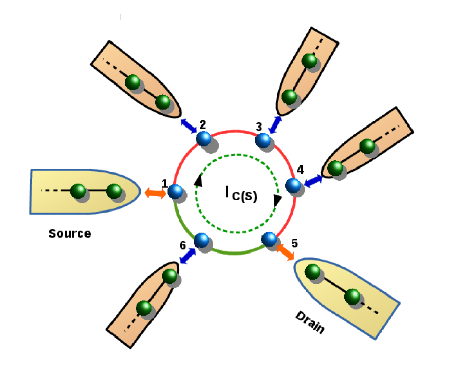
(i.e., four bonds) and three sites (i.e., two bonds). The scheme is that, imagine we have now two sets, where one set is a linear junction of five sites with , , and the dephasing leads are attached at the sites 2, 3 and 4. On the other hand, the other set, which is also linear, contains three sites where S and D are coupled at the two edges of the chain and the dephasing lead is attached at the middle point. Now, both for these two sets we determine the current densities following the steps given in the above two sub-sections (A and B) of this section, to get and . Using these current densities, we eventually calculate following the relation given in Eq. 14. Here it is important to note that the above mentioned two sets associated with the upper and lower arms of the ring are no longer decoupled with each other. When a bias is applied among S and D, an identical voltage drop () takes places at the ends of the two arms (viz, upper and lower) of the ring as they are connected in parallel. For the junction configuration given in Fig. 4, this voltage (i.e., ) is shared into four bonds for the upper arm, while it is shared into two bonds for the lower arm. Therefore, we can easily calculate for the two arms following the arguments as described above (Sec. IIIB).
Once the spin dependent circular density is found using Eq. 14, the net circular current at a bias voltage can be obtained from the relation cir5 ; cir6 ; cir9
| (15) |
where, is the equilibrium Fermi energy.
Finally, to check which spin dependent circular current is dominating in a particular bias window, we can define a quantity called as circular spin polarization as app5
| (16) |
where can be positive, or negative or even zero.
IV Accuracy of the analysis
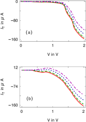
Before analyzing the results, it is important to check the accuracy of our
theoretical prescription, based on which we all the results are evaluated. In our prescription, we assume a linear dependence of the bias drop, and accordingly we determine the Büttiker voltages, though the finding of Büttiker voltages is somewhat non-trivial as it is a non-linear problem. To validate our linear approximation, in Fig. 5 we compute currents in all the Büttiker probes together with the drain current, considering a -site linear conductor like what is given in Fig. 3. Two different cases are shown depending on the strength of , and in both the cases clearly we see that the drain current (red curve) is much higher compared to the currents obtained in the Büttiker probes, even at much higher voltage bias. Thus, we can emphasize that our approximation is quite good and can safely be utilized to analyze the bias induced current phenomena, in presence of dephasing.
V Numerical Results and discussion
We analyze the results in two parts giving the emphasis on (1) circular current in a ring nanojunction in presence of Büttiker probes for the spin less case and then (2) extension of it in presence of spin dependent interaction. To explore the spin dependent phenomena, a clear understanding of spin independent case is definitely required.
Before starting to analyze the results, let us mention the parameter values those are common throughout the discussion. In the absence of any voltage bias, we set , and for the perfect ring , without loss of any generality. These site energies are modified in the presence of finite bias, following the prescription stated earlier. The impurities in the ring are included by choosing in the form of a correlated disorder one like aah1 ; aah2 ; aah3 ; aah4 ; aah5 , where measures the impurity strength and is an irrational number. We set (golden mean), though any other irrational number can equally be taken into account. Instead of ‘correlated’ disorder, one can also consider ‘uncorrelated’ (random) site energies to explore the effect of disorder, but in that case we have take the average over a large number of distinct disordered configurations. To avoid it, here we ignore random distribution, and with this consideration no physical picture will be changed in the context of present study. corresponds to the perfect ring. The hopping integrals are: , and . All the energies are measured in unit of electron volt (eV). The system temperature and the equilibrium Fermi energy are fixed at zero. For the entire calculation we couple the source electrode at site of the ring (viz, ).
V.0.1 In absence of spin dependent interaction
This sub-section focuses on the characteristic properties of circular charge current density (which sometimes may also be referred as charge current density without always recalling the term ‘circular’ for better readability), current densities in different segments along with transmission probability, in a ring nanojunction.
A. Charge current density, transmission probability and related issues:
Let us start with Fig. 6 where the variation of as a function of energy is shown both for the ordered and disordered cases at some typical values of dephasing strength . Several interesting features are observed, especially across the peaks and dips. To reveal these facts, we choose a region, shown by the dashed frame region, from each of the spectra given in Figs. 6(a) and (c), and the enlarged versions of these two regions are placed in the bottom row of Fig. 6, for better clarity of different colored curves. Apparently what we see from Figs. 6(a) and (c) that four picks and dips appear in each of the spectra. All these picks and dips are associated with the allowed energy channels of the system.
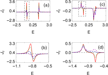
But actually the ring junction will have six resonant energy channels since we set which yields six distinct energy eigenvalues. For the ordered isolated ring the eigenvalues are , , , , and , i.e., the levels having eigenenergies or are two-fold degenerate, while the other two (i.e., and ) are non-degenerate. The energy channels associated with these eigenenergies get shifted with the inclusion of contact leads to the ring and/or adding impurities in the ring. Thus, from the information of discrete energy levels of the isolated rings, the approximate locations of the picks and dips can be estimated. A basic question that appears at this stage is that why no such peak or dip is observed at the other two energies i.e., around . To explain this fact, let us look into the spectra given in Fig. 7 where the current densities in the upper and lower arms of the ring are shown. Here we set , and with this result the non-vanishing behavior of at some typical energies for finite can also be understood. A tiny peak across appears for one arm, while a dip of almost equal strength is observed due to the other arm at these same energies of disorder-free ring (Fig. 7(a)). Naturally, around at , vanishingly small contribution in is obtained which is not visible in open eye from Fig. 6(a). Interestingly we see that, at the other energies the current densities for
both the two arms have identical sign (ve or ve), and hence it results a net circular current density. Identical scenario is also observed for the
disordered ring, apart from an overall suppression of the charge current densities in the arms (Fig. 7(b)). This reduction is associated with the disorder in the ring. From these results we can conclude that the sign reversal of current densities at the two extreme energy levels remains same for both the ordered and disordered rings, which yields almost zero contribution towards .
Now concentrate on the spectra given in Figs. 6(b) and (d). It is well known that transport current always decreases with disorder. Whereas, for the case of circular current the situation may be something different. The net circular current for a bias voltage is obtained by integrating the current density , over the energy window associated with the bias. Naturally, asymmetric nature of generates more current. For the energy window shown in Fig. 6(b) it is seen that a dip is followed by a neighboring peak and thus whenever we integrate over this energy window, the current will definitely decrease as it is the resultant contribution of picks and dips. For exactly equal and opposite contributions from different energy levels, the net current should be zero due to their mutual cancellations. An interesting feature noticed from Fig. 6(d) is that for the disordered case there is a finite possibility to have phase (i.e., sign of ) reversal in presence of , and thus instead of decreasing current with dephasing (as usually observed for the conventional transport current), one can get enhanced current since the successive peaks are of identical sign. Similar kind of enhancement can also be obtained for the perfect case, in presence of dephasing, depending on the junction configuration and other physical parameters, which will be understood from our further analysis.
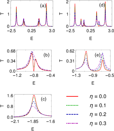
The nature of peaks and dips of circular current density (i.e., magnitude and sign) can be understood from the variation of transmission function. The results are presented in Fig. 8. Both for the ordered and
disordered cases large transmission appears for the two end energy levels, those are non-degenerate always for the isolated ring (be it ordered or disordered), where the peak height almost reaches to 2 (the factor 2 comes due to spin degeneracy). It means that at these energies transfer of electron is almost percent, and hence, very less contribution is obtained towards circular current, which is associated with the confining of electrons within the ring geometry. At these resonant energies, dephasing makes a suppression of peak heights which is clearly reflected by comparing the curves shown in Fig. 8(c) (zoomed region for a specific energy window across ). Across the energies , other many interesting features are observed and they become more fascinating in presence of dephasing. To reveal these facts, now focus on the spectra given in Figs. 8(b) and (e), those are zoomed versions of - spectra over a selective energy window for ordered and disordered cases, respectively. For , antiresonance appears around at in the absence of dephasing, where the transmission probability drops exactly to zero. This is the generic behavior of an asymmetrically connected interferometric geometry, and has also been been discussed in other contemporary works cir5 ; cir6 ; antr . The anti-resonant states disappear as long as dephasing leads are included (), and most interesting thing is that the hight of the transmission peaks gets increased with (see Fig. 8(b)). This enhancement of transmission leads to the reduction of circular current, as expected. The situation is somewhat complicated when is finite. Looking carefully
into Fig. 8(e), it is seen that for the two neighboring peaks the effect of is completely opposite. For one peak the hight decreases with , while it gets increased for the other one. This is solely associated with the interplay between disorder and dephasing. As a result of this there is a finite possibility to have phase reversal of at some typical energies which yields higher circular current, instead of its conventional reduction.
B. Size dependence and effect of ring-electrode interface geometry:
As quantum interference has significant impact on such properties (i.e., nature of circular current), it is therefore important to know how depends on the system size as well as different ring-drain configurations. This sub-section essentially focuses on that.
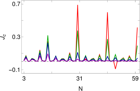
Figure 9 describes the dependence of on ring size . To have maximum contribution on , we couple the source and drain electrodes in the most asymmetric configuration. A pronounced oscillation with is observed both for the dephasing-free ring (red curve) and the ring with dephasing (green, blue and magenta curves). The oscillation is solely associated with the quantum interference among electronic waves passing through different arms of the junction. Interestingly what we see that at lower dephasing strength (), gets much higher peak in most of the cases compared to the dephasing-free ring, which clearly proves that one can get much higher circular current in presence of dephasing and it persists up to a reasonable ring size. For large enough , as the interference effect gets reduced the overall envelop of gradually decreases which is reflected by comparing the curves shown in Fig. 9.
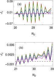
Figure 10 describes the dependence of ring-to-drain configuration on . Two different cases are considered depending on the ring size , odd and even, those are presented in Figs. 10(a) and (b), respectively.
Starting from the half-length of the ring, we gradually move the drain electrode towards the th site of the ring to examine the characteristics of . All these results are computed for a typical energy , though any other energy can also be selected. Both for even and odd , an oscillating nature is obtained, and the amplitude of oscillation strongly depends on the oddness and evenness of .
So eventually what we get from Figs. 9 and 10 that, is significantly influenced by quantum interference effect involving ring-electrode junction configuration and dephasing parameter .
C. Critical roles of and on circular current density:
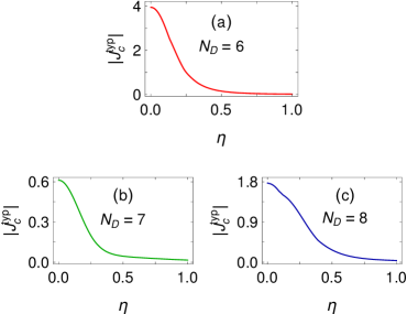
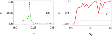
In order to have more clear signature of on we show the dependence of as a function of by varying it in a wide range, considering a ring of size . Three different cases are considered depending on , and the results are presented in Fig. 11. is obtained by taking the ‘maximum’ absolute value of over the full allowed energy window. In all the three cases, the over all signature of - curve looks identical, which suggest that for large enough , circular current is no longer available. This is essentially because of the fact that for large phase randomization becomes so strong which nullifies the effect of quantum interference.
Finally, we concentrate on Fig. 12, where the critical role of impurities on is shown. The interplay between dephasing () and disorder () is very interesting as clearly reflected in the spectra. For , increases suddenly and also rapidly decreases with , and it shows some irregular oscillation. With increasing , the fluctuation gradually decreases and almost ceases to zero for
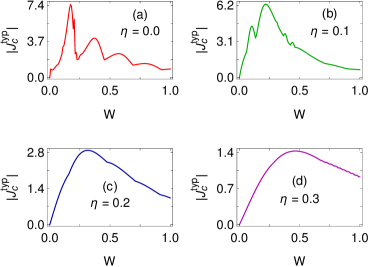
higher . This is expected as quantum fluctuations get diminished with because of the phase randomization. The key feature is that, here an enhancement of current density is observed, that will provide higher circular current, with impurity strength, which is no longer possible in the case of transport current (viz, the junction current) for the conventional disordered systems.
V.0.2 In presence of spin dependent interaction
Following the above analysis now we can explain the spin dependent phenomena and examine the critical role of dephasing, disorder, and ring-to-electrode junction configurations, etc., as the basic mechanisms are already discussed for the interaction-free ring nanojunction.
To discuss spin dependent features, we need to include spin-dependent scattering effect wg4 ; mag1 ; mag2 ; so1 ; so2 ; so3 in the system and that can be done in several ways. For instance, by considering a magnetic quantum ring or by using a Rashba ring, or by some other ways. In our discussion, we concentrate on the magnetic quantum ring where the ring contains finite magnetic moments having strength at each lattice sites, and their orientations can be described by the polar and azimuthal angles and , respectively, as used in conventional polar co-ordinate system. Due to these magnetic sites, a spin-dependent interaction appears in the Hamiltonian which yields an effective site energy term wg4 ; mag1 ; mag2 (). The rest part of the Hamiltonian will be unchanged. Here (=, , ) is the Pauli spin vector, and we assume is diagonal. Instead of magnetic quantum ring, one can also use Rashba ring or a junction with other kind of spin-dependent scattering mechanism, and the Hamiltonian will be changed accordingly. Our mathematical description can be well applied for any such systems.
In what follows we present our results for the spin-dependent case. For this entire section we choose , and for all sites , as a matter of simplification.
A. Spin dependent circular current, circular current densities and spin circular current:
Let us start with the spin dependent circular current ( and , evaluated by using Eq. 15) in a perfect magnetic quantum ring. The results are shown in Fig. 13 for some typical values of dephasing strength considering a 6-site ring where the
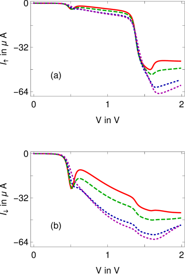
drain electrode is connected at 5th site. Several noteworthy features are observed from the spectra Fig. 13. At a first glance we see that for a wide bias window the current becomes zero, and the other notable thing is that here both the increasing and decreasing natures of current with voltage can be obtained. This reduction of current with bias is not usually observed for the case of conventional transport current, which always gets enhanced, provided NDR effect ndr is not there. We explain these phenomena as follows. The circular current is computed by integrating the current density over a suitable energy window associated with finite bias voltage. For a specific bias when no energy level appears in the energy window no contribution will be there which results vanishing current. With increasing the bias, the energy
window gets wider, and now if any energy level falls within this window a finite current appears. When more energy levels are accommodated, all of them contribute and a net current is the sum of all these contributing energy channels, which thus can be either mutually cancelled with each other or may be finite one, as different energy channels are contributing current in different directions (ve and ve). Here it is important to note that unlike conventional transport current, circular current can have both positive and negative signs depending on the contributing currents.
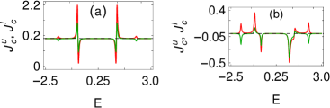
Along with the above facts more interesting patterns are also observed when we include impurities in the system. To reveal these facts look into the spectra given in Fig. 14 where the up and down spin currents are shown for a 6-site disordered ring setting . For a wide voltage bias currents are very small, associated with the appearance of the contributing energy channels, and beyond that regime, current increases rapidly with the bias.
The notable thing is that for a large voltage region the magnitudes of both and in the disordered ring are very large compared to the perfect one, which can be clearly noticed by comparing the spectra shown in Figs. 13 and 14. This is solely associated with the current density profile of the junction. For the ordered case the resonant picks and dips are comparatively symmetric than the disordered one. More symmetric picks and dips naturally produce lesser net current. Thus to have higher circular current we need to have more asymmetric current density profile. So what emerges from Fig. 14 is that, in presence of disorder higher spin dependent current can be obtained in different voltage windows. At the same time it is also possible to have one phase of current (ve or ve) for a wide bias voltage.
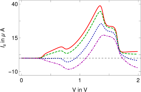
From the variations of and , as given in Fig. 13 and Fig. 14, an obvious question arises that how spin circular current varies as a function of bias voltage.
The answer is given in Fig. 15, where we show the variation of spin current for the same junction set up as taken in Fig. 14. The interplay between the disorder and environmental dephasing is undoubtedly interesting. The complete phase reversal along with enhancement of spin current can be achieved by selectively choosing the bias voltage and other physical parameters describing the system.
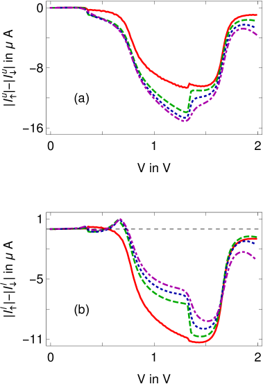
From the above discussion it is now clear that a situation may happen when in one arm the up spin current dominates the down spin current, whereas the phenomenon gets reversed in the other arm. The best performance can be achieved when the less contributing spin currents are fully suppressed, so that different arms will carry pure spin currents without mixing between and . Under this situation informations can be transferred selectively through different segments of a nanojunction having multiple paths. Figure 16 describes such a possibility, where we show the variation of in the two different arms at some typical values of dephasing strength , where the meaning of different colored curves are the same as described earlier. The dephasing factor affects the current in different ways in the two arms. In the upper arm the magnitude of gets increased with , while an opposite scenario is noticed in the other arm. These features are reflected in the net circular spin current.
B. Polarization coefficient:
Finally, we discuss the phenomenon of polarization coefficient that is calculated by using Eq. 16 to understand which one among and dominates for different input conditions. The results are shown in Fig. 17. Let us first concentrate on Fig. 17(a). It is clearly seen that the polarization is significantly influenced by the dephasing strength . For a fixed drain position, can be changed in a wide range, and in some cases it may even reach to cent percent. At the same time, for a fixed , a complete phase reversal of can
also be made by altering the drain position . Thus, the interplay between the environmental dephasing and ring-to-electrode junction configuration is extremely important to have the polarization or more precisely to characterize spin dependent circular currents. The role of is further examined by changing it in a wider range considering a bigger ring (see Fig. 17(b)). The overall conclusion remains same. Under certain input conditions we can have net circular current completely due to one components among and , circumventing the mixing between them.
VI Concluding Remarks
We have proposed a new concept of bias induced circular currents in a ring nanojunction in presence of impurities and environmental dephasing where dephasing is introduced in the form of Büttiker probes, that may opens up the possibilities of designing spintronic devices and proper spin regulation. We have given a detailed theoretical prescription for calculating spin dependent current density satisfying all the conservation rules in presence of phase randomizing leads. Our analysis can be generalized in any system with any kind of spin dependent scattering. The theoretical prescription in presence of phase randomizing leads has not been discussed, even in the context of charge circular current, so far in literature to the best of our knowledge.
We have critically examined the characteristic features of current densities, branch currents, circular currents and polarization both in absence and presence of spin dependent interaction, and discussed thoroughly the interplay between the impurities and dephasing on these quantities. The key findings are summarized as follows.
The energy levels for which electronic transmission is very high, close to the ballistic nature, the contribution towards circular current is too small due to less confining within the loop.
Even for the disordered case, a high degree of enhancement in current along with the phase reversal is possible with . Though for large enough current should vanish due to complete phase randomization.
The circular current is highly sensitive to the ring-electrode junction configuration. A pronounced oscillation has been observed.
Finally, from the analysis of polarization co-efficient it can be inferred that under certain physical conditions circular current is possible purely due to or , avoiding any mixing between them.
VII Acknowledgments
SKM would like to acknowledge the financial support of DST-SERB, Government of India, under the Project Grant No. EMR/2017/000504. SKM is also very much thankful to the fruitful conversation about different topics discussed in this work with Prof. Abraham Nitzan during the visit of SKM at Tel Aviv University, Israel. MP and SKM would like to thank all the reviewers for their constructive criticisms, valuable comments and suggestions to improve the quality of the work.
Appendix A Coupled equations to calculate transmission probability and current density in absence of spin degree of freedom, considering the Büttiker probes as the input leads
For the set up presented in Fig. 3, let us consider the lead-1 (Büttiker probe) as the input lead. Under this situation the coupled equations are expressed as follows.
Similarly, the coupled equations for the other Büttiker probe (viz, lead-2), which can act as the input lead, are as follows.
| (18) | |||||
So, bond current densities between the sites and , when the Büttiker probes and are taken as input leads, are:
| (19) | |||||
and,
| (20) | |||||
respectively.
Appendix B Coupled equations to calculate transmission probability and current density in presence of spin degree of freedom, considering the source as the input lead
For the junction configuration given in Fig. 3, the set of coupled equations, in presence of spin degree of freedom, considering source S as the input lead where electrons with up spin are injected, can be expressed as follows.
| (35) | |||
| (50) | |||
| (65) | |||
| (70) | |||
| (85) | |||
| (90) | |||
| (105) | |||
| (120) | |||
| (135) | |||
| (150) | |||
| (151) |
Similarly, for the down spin incidence the equations are:
| (166) | |||
| (181) | |||
| (196) | |||
| (201) | |||
| (216) | |||
| (221) | |||
| (236) | |||
| (251) | |||
| (266) | |||
| (281) | |||
| (282) |
The factors and used in these expressions correspond to the transmission and reflections amplitudes, respectively, for an electron with spin which is transmitted and/or reflected as spin .
References
- (1) A. Nakanishi and M. Tsukada, Phys. Rev. Lett. 87, 126801 (2001).
- (2) K. Tagami and M. Tsukada, Curr. Appl. Phys. 3, 439 (2003).
- (3) M. Tsukada, K. Tagami, K. Hirose, and N. Kobayashi, J. Phys. Soc. Jpn. 74, 1079 (2005).
- (4) G. Stefanucci, E. Perfetto, S. Bellucci, and M. Cini, Phys. Rev. B 79, 073406 (2009).
- (5) D. Rai, O. Hod, and A. Nitzan, J. Phys. Chem. C 114, 20583 (2010).
- (6) D. Rai, O. Hod, and A. Nitzan, Phys. Rev. B 85, 155440 (2012).
- (7) S. K. Maiti, Eur. Phys. J. B 86, 296 (2013).
- (8) S. K. Maiti, J. Appl. Phys. 117, 024306 (2015).
- (9) M. Patra and S. K. Maiti, Sci. Rep. 7, 43343 (2017).
- (10) U. Dhakal and D. Rai, J. Phys.: Condens. Matter 31, 125302 (2019).
- (11) M. Büttiker, Y. Imry and R. Landauer, Phys. Lett. A 96, 365 (1983).
- (12) H.-F. Cheung, Y. Gefen, E. K. Riedel and W. H. Shih, Phys. Rev. B 37, 6050 (1988).
- (13) L. P. Levy, G. Dolan, J. Dunsmuir and H Bouchiat, Phys. Rev. Lett. 64, 2074 (1990).
- (14) H. Bluhm, N. C. Koshnick, J. A. Bert, M. E. Huber and K. A. Moler, Phys. Rev. Lett. 102, 136802 (2009).
- (15) S. K. Maiti, M. Dey, S. Sil, A. Chakrabarti, and S. N. Karmakar, Europhys. Lett. 95, 57008 (2011).
- (16) S. Nakanishi and M. Tsukada, Surf. Sci. 438, 305 (1999).
- (17) L. Wang, K. Tagami, and M. Tsukada, Jpn. J. Appl. Phys. 43, 2779 (2004).
- (18) D. Loss and D. P. DiVincenzo, Phys. Rev. A 57, 120 (1998).
- (19) E. B. Kane, Nature 393, 133 (1998).
- (20) G. Burkard, D. Loss, and D. P. DiVincenzo, Phys. Rev. B 59, 2070 (1999).
- (21) R. Vrijen, E. Yablonovitch, K. Wang, H. W. Jiang, A. Balandin, V. Roychowdhury, T. Mor, and D. DiVincenzo, Phys. Rev. A 62, 012306 (2000).
- (22) D. Rai and M. Galperin, Phys. Rev. B 86, 045420 (2012).
- (23) M. Patra and S. K. Maiti, Europhys. Lett. 121, 38004 (2018).
- (24) M. Patra and S. K. Maiti, Org. Electron. 62, 454 (2018).
- (25) Yu. V. Pershin and C. Piermarocchi, Phys. Rev. B 72, 245331 (2005).
- (26) D. A. Lidar and J. H. Thywissen, J. Appl. Phys. 96, 754 (2004).
- (27) M. Büttiker, Phys. Rev. Lett. 57, 1761 (1986).
- (28) M. Büttiker, IBM J. Res. Dev. 32, 63 (1988).
- (29) A.-M. Guo and Q.-F. Sun, Phys. Rev. Lett. 108, 218102 (2012).
- (30) M. Patra, S. K. Maiti, and S. Sil, J. Phys.: Condens. Matter 31, 355303 (2019).
- (31) M. Patra and S. K. Maiti, J. Magn. Magn. Mater. 484, 408 (2019).
- (32) V. B.-Moshe, A. Nitzan, S. S. Skourtis, and D. N. Beratan, J. Phys. Chem. C 114, 8005 (2010).
- (33) V. B.-Moshe, D. Rai, S. S. Skourtis, and A. Nitzan, J. Chem. Phys. 133, 054105 (2010).
- (34) S. Datta, Electronic Transport in Mesoscopic Systems, Cambridge University Press, Cambridge (1997).
- (35) S. Datta, Quantum Transport: Atom to Transistor, Cambridge University Press, Cambridge (2005).
- (36) C.-M. Ryu, S. Y. Cho, M. Shin, K. W. Park, S. Lee, and E.-H. Lee, Int. J. Mod. Phys. B 10, 701 (1996).
- (37) Y. Shi and H. Chen, Phys. Rev. B 60, 10949 (1999).
- (38) Y. -J. Xiong and X. -T. Liang, Phys. Lett. A 330, 307 (2004).
- (39) M. Patra and S. K. Maiti, Sci. Rep. 7, 14313 (2017).
- (40) M. Mardaani, A. A. Shokri, and K. Esfarjani, Physica E 28, 150 (2005).
- (41) M. Dey, S. K. Maiti, and S. N. Karmakar, Eur. Phys. J. B 80, 105 (2011).
- (42) S. Sil, S. K. Maiti, and A. Chakrabarti, Phys. Rev. Lett. 101, 076803 (2008).
- (43) T.-R. Pan, A.-M. Guo, and Q.-F. Sun, Phys. Rev. B 92, 115418 (2015).
- (44) S. Souma and B. K. Nikolić, Phys. Rev. Lett. 94, 106602 (2005).
- (45) J. R. Brews and C. J. Hwang, J. Chem. Phys. 54, 3263 (1971).
- (46) P. F. Bagwell and T. P. Orlando, Phys. Rev. B 40, 1456 (1989).
- (47) G. B. Lesovik and I. A. Sadovskyy, Phys. Usp. 54, 1007 (2011).
- (48) D. A. Ryndyk, Theory of Quantum Transport at Nanoscale, Springer (2016).
- (49) S. Aubry and G. André, Ann. Isr. Phys. Soc. 3, 133 (1980).
- (50) Y. Lahini, R. Pugatch, F. Pozzi, M. Sorel, R. Morandotti, N. Davidson, and Y. Silberberg, Phys. Rev. Lett. 103, 013901 (2009).
- (51) Y. E. Kraus, Y. Lahini, Z. Ringel, M. Verbin, and O. Zilberberg, Phys. Rev. Lett. 109, 106402 (2012).
- (52) S. Ganeshan, K. Sun, and S. Das Sharma, Phys. Rev. Lett. 110, 180403 (2013).
- (53) S. K. Maiti, S. Sil, and A. Chakrabarti, Ann. Phys. (N. Y.) 382, 150 (2017).
- (54) M. Patra and S. K. Maiti, Phys. Lett. A 382, 420 (2018).
- (55) A. A. Shokri, M. Mardaani, and K. Esfarjani, Physica E 27, 325 (2005).
- (56) A. A. Shokri and M. Mardaani, Solid State Commun. 137, 53 (2006).
- (57) Yu. A. Bychkov and E. I. Rashba, JETP Lett. 39, 78 (1984).
- (58) G. Dresselhaus, Phys. Rev. 100, 580 (1955).
- (59) M. Patra and S. K. Maiti, Eur. Phys. J. B 89, 88 (2016).
- (60) A. Z. Thong, M. S. P. Shaffer, and A. P. Horsfield, Sci. Rep. 8, 9120 (2018).