Engineering electron-phonon coupling of quantum defects to a semi-confocal acoustic resonator
Abstract
Diamond-based microelectromechanical systems (MEMS) enable direct coupling between the quantum states of nitrogen-vacancy (NV) centers and the phonon modes of a mechanical resonator. One example, diamond high-overtone bulk acoustic resonators (HBARs), feature an integrated piezoelectric transducer and support high-quality factor resonance modes into the GHz frequency range. The acoustic modes allow mechanical manipulation of deeply embedded NV centers with long spin and orbital coherence times. Unfortunately, the spin-phonon coupling rate is limited by the large resonator size, m, and thus strongly-coupled NV electron-phonon interactions remain out of reach in current diamond BAR devices. Here, we report the design and fabrication of a semi-confocal HBAR (SCHBAR) device on diamond (silicon carbide) with (). The semi-confocal geometry confines the phonon mode laterally below 10 m. This drastic reduction in modal volume enhances defect center electron-phonon coupling. For the native NV centers inside the diamond device, we demonstrate mechanically driven spin transitions and show a high strain-driving efficiency with a Rabi frequency of MHz/Vp, which is comparable to a typical microwave antenna at the same microwave power.
keywords:
Nitrogen-vacancy center, diamond, silicon Carbide, acoustic resonator, electron-phonon coupling, MEMSCornell] Cornell University, Ithaca, New York 14853, United States Purdue] Purdue University, West Lafayette, Indiana 47907, United States Purdue] Purdue University, West Lafayette, Indiana 47907, United States Cornell] Cornell University, Ithaca, New York 14853, United States Cornell] Cornell University, Ithaca, New York 14853, United States Purdue] Purdue University, West Lafayette, Indiana 47907, United States Cornell] Cornell University, Ithaca, New York 14853, United States \alsoaffiliation[Kavli] Kavli Institute at Cornell for Nanoscale Science, Cornell University, Ithaca, New York 14853, United States \abbreviationsNV, MEMS, SiC
Defect-based qubits are attractive platforms for solid state quantum technologies1. The leading examples are the nitrogen-vacancy (NV)2 center and the silicon-vacancy (SiV)3 center in diamond, and the divacancy center4 and the silicon vacancy center (V)5 in silicon carbide (SiC). Hybrid quantum systems based on these defect qubits are particularly interesting because they interface the qubit spin to photons or phonons and thus potentially enable the transport of quantum information. For sensing applications, they offer unconventional modalities of quantum control which is a resource for extending the coherence time and thus sensitivity. Coupling spins to mechanical motion could also enable new quantum-enhanced sensors of motion, such as inertial sensing6, 7.
Although solid state spin-photon entanglement has been demonstrated in recent years8 and has been used to build quantum networks9, defect-based spin-mechanical systems have yet to operate at the single phonon quantum level because they are limited by weak electron-phonon coupling, , in existing devices. Considering , where is the modal volume, one approach to strengthening the coupling is to engineer small mode volume mechanical resonators with high quality factors. Ultimately, defect-based spin-mechanical systems may enable new sensing applications and control of phonon states at the quantum level10.
Defect-based spin-mechanical systems can be classified into two categories: 1) micro-beam resonator systems11, 12, 13 and 2) micro-electromechanical systems (MEMS)14, 15, 16, 17 with integrated thin-film piezoelectric transducers. While the first category minimizes the resonator fabrication to a single material, i.e., diamond, SiC, etc., high-frequency micro-beam resonators (1 GHz) are difficult to efficiently excite and detect. The latter category includes surface acoustic wave (SAW) and bulk acoustic wave (BAW) devices. These resonator types can be excited and characterized electrically, and they enable both quantum circuit integration 10, 18 and direct quantum control of embedded defect qubits. At higher frequency (2 GHz), while SAW devices start to show progressively higher losses, BAW resonators maintain a high quality factor19. Additionally, BAW resonator can couple to defect centers that lie deep inside the device, making them less susceptible to deleterious surface effects and thus they can possess long spin and orbital coherence times.
Here we report the design, fabrication and performance of a new type of diamond (and SiC) BAW device, the semi-confocal high-overtone bulk acoustic resonator (SCHBAR). The device features a micro-scale phonon mode volume and integrated atomic-scale quantum defects. Electrical measurements show that the frequency-quality factor product is () for diamond (SiC) SCHBAR devices operating with a 3 GHz phonon mode. In a diamond SCHBAR device, we use the native NV centers to characterize the a.c. strain performance of the acoustic resonator. We mechanically drive NV center ground-state spin Rabi oscillations at a rate MHz/Vp, corresponding to a mechanical strain , indicating high power-to-strain conversion efficiency. Applications of this device include the fast quantum control of defect spins in the double-quantum basis, study of spin dynamics in the strong-mechanical-driving regime, and quantum control of resonator states using dense defect spin ensembles.
BAW devices have been widely used in the microelectronics industry for RF filtering and other wireless applications20. The transducer of most BAW devices consists of a piezoelectric thin film sandwiched between two electrodes in a released structure or solidly mounted on a planar substrate. The two planar boundaries of the device form a cavity for the bulk acoustic wave. To achieve a high quality factor, a high degree of parallelism for the two planar boundaries is stringently required to suppresses the acoustic diffraction loss21. Even with perfectly parallel boundaries, a planar cavity lacks lateral confinement22. A partial solution is to make large area transducer to spatially limit the diffraction loss, however, this also constrains the size scale of a standard BAW device to be larger than m.
In analogy to a confocal or semi-confocal optical cavity, an acoustic cavity with curved boundaries that match the wavefront of the acoustic wave can overcome diffraction loss and provide stable mode confinement. The cavity stability criterion suggests that the best confinement is obtained in a confocal geometry or a semi-confocal geometry for a planar convex boundary condition. The idea has been demonstrated recently in both SAW23, 24, 17 and BAW devices25, 26 at millimeter scale. Here we apply this concept to a micro-scale BAW resonator. We choose to work with diamond and SiC substrates because they possess excellent mechanical properties and their crystal lattices host quantum defects. We design the micro resonator for a 10- and a 20-m-thick device.
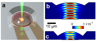
As illustrated in Fig. 1(a), the device has a planar-convex structure. We design one side of the resonator with a curved surface, enabling it to confine three dimensional phonon modes with characteristic dimensions of 10 m. The radius of curvature of the curved surface is twice the thickness of the substrate in a semi-confocal geometry, giving rise to the device name, SCHBAR. Compared to a planar cavity, the curved surface eliminates the requirement of boundary parallelism and, in principle, yields higher mechanical quality factors. Optically, the curved surface also acts as a solid immersion lens (SIL). It reduces substrate refraction and thus enhances light extraction from the defects inside the resonator27. The defects are microns below the surface and thus are well-protected from fabrication damage and surface effects. On the planar side of the device, we fabricate an integrated piezoelectric transducer and a microwave antenna that is aligned with the center of the resonator, allowing for acoustic and magnetic driving, respectively. The radius of the transducer has been designed to mode-match the waist of the confined acoustic wave, and the thickness of piezoelectric ZnO film is controlled to target a 3 GHz resonance mode which allows stable confinement.
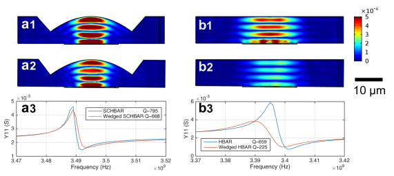
We simulate the mechanical performance of the device using COMSOL. Fig. 1(b) and (c) show the strain profile of a 3 GHz acoustic mode for a 20 and a 10 m device, with a driving voltage amplitude at V. The simulation results show stable confinement of the acoustic wave and a peak strain around .
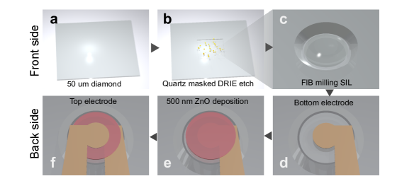
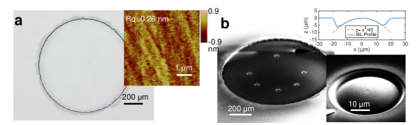
We fabricated SCHBAR devices from both diamond and 4H-SiC substrates28. For simplicity, here we restrict the process flow description to diamond, as presented in Fig. 2. We start from a 50-m-thick, double-side polished single crystal diamond plate (nitrogen concentration ppm). In the first step, we etch m of diamond on each side of the substrate using Ar/29 and plasma30, 31, 32 as a stress-relief etch to eliminate the residual polishing damage (see Supporting Information). A laser-cut quartz shadow mask is then used to mask the diamond for another 20- or 30-m-deep etch on one side of the sample (etch rate m/hr). After lifting the quartz mask, we end up with a 10 m or 20 m diamond membrane suspended in a 40 m frame. Atomic force microscopy (AFM) shows a surface roughness of 0.3 nm. A focused gallium ion beam (FIB, 30 kV, 20 nA) is used to mill the parabolic SIL structure on the diamond membrane. After FIB milling, the diamond surface is substantially graphitized and contains implanted gallium atoms (20 nm in depth)33. We then etch away the top 100 nm of damaged diamond using Ar/ plasma, followed by a 120 nm plasma etch to oxygen terminate the diamond surface. A boiling tri-acid bath containing equal parts of sulfuric, nitric and perchloric acid is used to further clean off any residual contamination on the diamond. Optical profilometry and laser-scanning confocal microscopy have been used to confirm the profile accuracy of the SIL. The diamond membrane is then flipped with the planar side facing up. A piezoelectric zinc oxide (ZnO) transducer, consisting of bottom electrode (10 nm/90 nm Ti/Pt), 500 nm ZnO, top electrode (10 nm/180 nm Ti/Pt), and a microwave antenna are then lithographically defined and sputtered to finish the device fabrication.
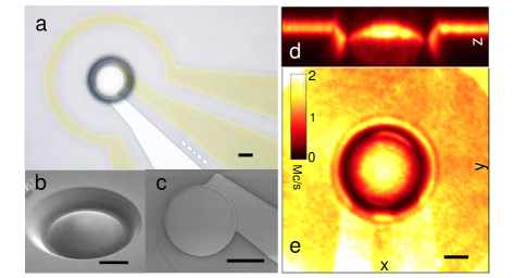
Fig. 3(a-c) show the images of a finished diamond device. We measure the photoluminescence (PL) of the NV center ensemble inside the diamond SCHBAR using a home-built confocal microscope, where a 532 nm laser is used for excitation and a 630 nm long pass filter is used for PL collection in the phonon side band emission of NV centers. Fig. 3(d-e) show the cross section and the front PL scan of a 10 m device at an incident laser power of 150 W. There is a clear enhancement of PL collection inside the resonator. This, in combination with the spin measurement reported later in the letter, confirms that the NV centers are intact after fabrication.
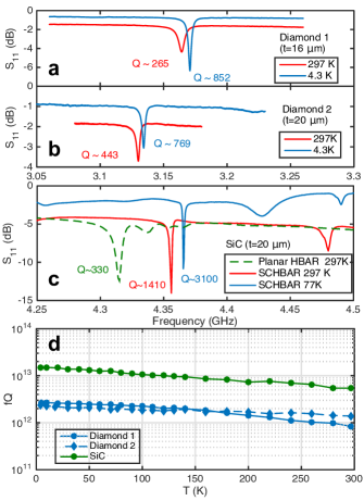
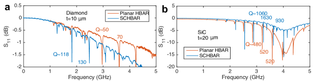
The device is then wire-bonded to a circuit board for electrical measurement. A vector network analyzer (VNA) is used to characterize the scattering parameter (S-parameter) of the device. When the resonator is driven on resonance, microwave power is dissipated in the resonator and converted into mechanical energy, launching acoustic waves and enabling the resonance to be detected as a decrease in the reflected microwave power. The electromechanical response of the device is well described by the modified Butterworth Van-Dyke model34, and the mechanical quality factor, , can be extracted from the VNA measurements. After mounting the devices in vacuum on a cold finger of a helium-flow cryostat, we perform electrical measurements as a function of temperature. The results are shown in Fig. 4. The frequency and quality factor product is for a 20-m-thick diamond device at room temperature and for a 20-m-thick SiC device at low temperature. For the SiC device, we change the order of fabrication to enable a test of the Q-enhancement due to the curved acoustic mirror. In this case, we mill the SIL after the piezoelectric transducer fabrication, enabling a separate measurement of both a planar and a semi-confocal version of the same device. We find a 3x improvement in the quality factor with the addition of the SIL. We have also found similar effects in 10-m-thick diamond devices (see Supporting Information), indicating that the additional acoustic confinement adds in the suppression of acoustic diffraction loss. Theoretically35, 36, 37, 38, 39, 40, the quality factor of the current diamond device is limited by phonon scattering, at room temperature (see Supporting Information), which is an order of magnitude higher than the measured value. Possible sources for the extra damping can be surface dissipation and material losses within the piezoelectric transducer, which are not included in our estimate.
Next we characterize the defect spins in the resonator and their coupling to the phonon mode. Although we detected silicon vacancy (V) center emission in the SiC device (see Supporting Information), indicating the possibility of acoustic control of defect system in SiC, here we focus on NV center spin measurements using a diamond SCHBAR.
At room temperature, both the ground and the excited states of an NV center are spin triplets. The ground-state electron spin state degeneracy can be lifted via their coupling to magnetic and strain fields (Fig. 4(a)), depicted by the Hamiltonian2:
| (1) |
where GHz is the zero-field splitting, = MHz/G is the gyromagnetic ratio, is the electron spin of an NV center (), is the spin coupling strength to the transverse (longitudinal) strain field . Three sets of qubits can therefore be formed: magnetically-driven single quantum spin transitions between and states, and the mechanically-driven double quantum spin transition between states14. We use the latter one to quantitatively characterize the resonator performance and to study the defect electron-phonon coupling in a diamond SCHBAR device.
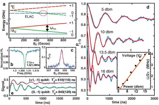
All measurements are made at room temperature using a 20-m-thick diamond SCHBAR. We first apply an external magnetic field of 558.6 G, axially aligned to the N-V axis. This splits the and ground spin states of the NV center ensemble due to the Zeeman effect (Fig. 4(a)). At 558.6 G, the spin and state separation is in resonance with the phonon mode frequency, . We then launch acoustic waves in the resonator by applying microwave power to the transducer at the resonator frequency 3.13 GHz. Coherent spin transitions can thus be induced by the acoustic wave through the transverse spin-strain coupling14, 41.
Note that the operating magnetic field strength is close to the excited-state level anti-crossing (ELAC) at 508 G42. By optical pumping in a well-aligned magnetic field, we can induce a strong polarization of the nuclear spin of 14N into its state (Fig. 4(b)). By working with only a single hyperfine state, we greatly improve the signal-to-noise ratio and reduce the complexity of the system dynamics.
Now we test the mechanical driving efficiency and coherence. To pinpoint the mechanically-driven spin resonance, we perform optically detected mechanical spin resonance (ODMSR) measurements as described in Ref. 14 (see Supporting Information). We observe a single resonance peak in the spectrum, confirming the strong nuclear spin polarization within the NV center ensemble. We then perform mechanically-driven Rabi measurements of the and states as a function of microwave power applied to the transducer. We observe high contrast Rabi oscillations at a rate MHz/Vp, where Vp is the peak voltage applied to the input port of our device. Transverse NV center spin-strain coupling, , has been previously measured at around 20 GHz/strain11, 43, enabling us to estimate that the current device has a high power-to-strain efficiency of (see Supporting Information). This value is close to the COMSOL simulation result, and compared to an HBAR device41, the power-to-strain efficiency has improved by 60-160x. Lastly, we measure the spin coherence within the mechanically-controlled , subspace and within the magnetically-controlled , subspace (Fig. 5(e)). We find is 610(110) ns and 840(120) ns, respectively.
With the demonstrated voltage-to-strain transduction, the diamond SCHBAR device has roughly the same efficiency for spin-strain driving as the microwave antenna has for magnetic driving. This is promising for using mechanical driving as an added resource, for example, strong mechanical driving of NV center spins can be used to extend the coherence time via continuous dynamical decoupling44, 45. Additionally, the ability to perform pulsed spin control protocols within the , subspace, which are enabled by sizable Rabi frequencies and 40 ns ring-up/down times, makes quantum control a strong application of our device. These capabilities will be a useful resource for magnetic sensing in the double-quantum basis46 and for non-magnetic sensing modalities such as inertial sensing6. Apart from fast mechanical control of defect spins, a SCHBAR operates at a high enough frequency to be cooled to its mechanical ground state using a dilution refrigerator ( 100 mK). In combination with spin ensemble enhancement to phonon coupling, the device can potentially be used for studying spin-phonon coupling at a single phonon level47 (see Supporting Information). Improvements to the device quality factors and power handling are possible by replacing ZnO with AlN. Further enhancement in single spin-phonon coupling can be obtained by further reduction of the device volume, however, it must accompany a shift to a higher resonator frequency. An alternative approach is to incorporate color centers with intrinsically stronger spin-phonon coupling, such as the diamond SiV center48.
In conclusion, we report the design, fabrication and testing of a diamond (SiC) SCHBAR device. SCHBAR marks the first step towards a micro-scale BAW resonator device. We obtain for a diamond (SiC) SCHBAR and demonstrate efficient and high-rate phonon-induced NV center Rabi oscillations at MHz/Vp. The device enables direct circuit integration and it is ideal for fast mechanical control of defect spins. Further integration of a dense spin ensemble along with improvements in the device quality factor could enable study of defect spin-phonon interaction at the quantum level.
Research support was provided by the Office of Naval Research (Grant N000141712290) and by the DARPA DRINQS program (Cooperative Agreement D18AC00024). Any opinions, findings, and conclusions or recommendations expressed in this publication are those of the author(s) and do not necessarily reflect the views of DARPA. R.S.D. acknowledges support of the Air Force Office of Scientific Research Hybrid Materials MURI under award number FA9550-18-1-0480. Device fabrication was performed in part at the Cornell NanoScale Science and Technology Facility, a member of the National Nanotechnology Coordinated Infrastructure, which is supported by the National Science Foundation (Grant ECCS-15420819), and at the Cornell Center for Materials Research Shared Facilities which are supported through the NSF MRSEC program (Grant DMR-1719875).
1 Supporting Information
Engineering electron-phonon coupling of quantum defects to a semi-confocal acoustic resonator
2 SCHBAR VS HBAR
We compare the performance of an SCHBAR to an HBAR using COMSOL modeling. Fig. 6 shows the simulation results of a 10--thick planar HBAR and a 10--thick SCHBAR device with a 1 Vp drive, where Vp is peak voltage. In comparison to the planar HBAR, the SCHBAR has stronger phonon mode confinement and a larger strain amplitude. An important factor that determines the performance of an HBAR device is the surface parallelism. A slight thickness variation across the substrate can lead to significant phonon leakage and a reduced quality factor. In Fig. 6(a-b2), we introduce a 0.46 degree tilt angle (0.4 m thickness variation across 50 m) to one surface of the substrate. In contrast to the drastic decrease of quality factor in an HBAR device, there is little impact on the SCHBAR -factor from the substrate thickness variation. This is beneficial for diamond devices because it alleviates the stringent requirement for alignment in substrate polishing which helps to achieve a high quality factor.
3 Optical collection efficiency enhancement
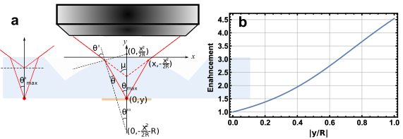
Using a ray optics calculation, we numerically solve the collection solid angle as a function of depth in the device. At the critical angle, the exit ray angle matches the numerical aperture of the lens, . The schematics is shown in Fig. 7(a), with the following constraints applied:
| (2) |
where is the radius of curvature of the SIL at , is the substrate refractive index, is the depth inside the SIL.
The solution of can be numerically solved, and the maximum collection angle is . Compared to a planar structure, , the enhancement in fluorescence collection is shown in Fig. 7(b), evaluated as .
4 Diamond etching and characterization
We use Ar/Cl229 combined with O2 plasma to etch diamond. Mechanically polished diamond surfaces have micro-scale defects (particles and pits) and polishing streaks from the lapping process. Without proper treatment, O2 plasma tends to etch anisotropically around the defects, leaving either a grass-like rough surface or pitted surface with craters30. Ar/Cl2 etches diamond isotropically and can effectively remove the surface contaminants, smoothening the diamond surface32. To compensate for the slow etch rate of Ar/Cl2 plasma, we switch to O2 plasma after Ar/Cl2 plasma etch and alternate to Ar/Cl2 plasma intermittently for a short time to remove possible surface contamination31 from, for instance, sputtered particles in the etcher chamber. Detailed operating parameters for diamond etch are listed in Table. 1-2.
| Gas | Flow rate | Pressure | ICP/RIE | DC bias | etch rate | Selectivity to SiO2 |
|---|---|---|---|---|---|---|
| (sccm) | (mTorr) | (W) | (V) | (nm/min) | ||
| Ar/Cl2 | 25/40 | 8 | 600/100 | 217 | 34(1) | 0.72 |
| O2 | 60 | 10 | 950/50 | 132 | 118(2) |
| Etch Type | Process | Etch rate/depth (include plasma off time) |
|---|---|---|
| Stress relief | 35 min Ar/Cl2+20 min O2 | 4.9 m |
| +5 min Ar/Cl2+10 min O2 | ||
| DRIE | 5 min Ar/Cl2+20 min O2 | 5 m/hr |
| Post FIB clean | 3 min Ar/Cl2+1 min O2 | 220 nm |
After quartz masked diamond etch, we perform optical profilometry (Zygo NewView 7300) to measure the etch depth and use a laser scanning confocal microscope (Keyence VK-X260) for membrane thickness characterization. After etching, AFM measurement shows that the surface roughness is less than 0.3 nm (Fig. 8).
5 Quality factor limit analysis
In general, the quality factor of a mechanical resonator can be determined from various sources: 1) air damping, 2) clamping loss, 3) thermoelastic dissipation (TED), 4) phonon scattering, 5) lattice friction from crystalline defect, etc. While air damping is negligible in a sufficiently high-frequency resonator and can be eliminated by operating in vacuum, the rest require careful design and engineering to minimize. Clamping loss arises when the resonator anchor is stressed and can thus be avoided by designing the resonator to have a stress-free boundary, such as a tuning fork. In our SCHBAR, the boundary is close to a stress free condition from the SIL confinement. TED occurs due to the strain-gradient-induced heat flow inside resonator. A few approaches have been demonstrated to address TED: 1) design a resonator with isotropic strain or a pure shear mode resonator that has no volume change, 2) operate in an environment where the thermal expansion coefficient of the resonator material is zero, 3) block heat flow by cutting slots in a beam resonator, 4) operate resonator at a frequency away from the thermalization rate, 40. For low-frequency beam resonators, TED can be a major limiting factor to the quality factor at 100 K and above. Lifshitz40 derived the exact solution of TED based on Zener’s work35,
| (3) |
where is the heat capacity per unit volume, is the specific heat, is the Young’s modulus of the material, is the thermal expansion coefficient at temperature . , is the thermal relaxation time, is the width of the beam, is the thermal conductivity.
For a high-frequency (here 3 GHz) bulk acoustic wave resonator (equivalently an infinitely thick beam resonator), acoustic attenuation caused by TED is significantly less because of a longer thermalization time, , exceeded by resonator frequency (applies for K), . The theoretical limit of Q is derived for a longitudinal wave in an isotropic media by Landau39,
| (4) |
where and are shear and longitudinal speed of sound.
While the TED limit for a bulk acoustic wave device is high, for diamond at 300 K (Fig.9(a)), phonon scattering process enforces another fundamental limit to the quality factor, theorized by Akhiezer37, Landau and Rumer36, 49:
| (5) |
where is the Grneisen’s parameter, is the phonon relaxation time. is Plank constant, is Boltzmann constant. Note that Woodruff’s result is 1.5 times higher than Maris’s at low frequency, and transits to the same frequency scaling as Landau-Rumer’s result for high frequency regime (Fig. 9(b)).
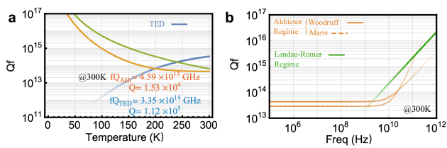
For a 3 GHz diamond SCHBAR, at room temperature, close to the transition from Akhiezer regime to Landau-Rumer regime, as shown in Fig. 9(b). The quality factor limit is set by phonon-phonon interactions, at room temperature, an order of magnitude higher than our measurement in the fabricated diamond SCHBAR. We attribute possible quality factor limiting sources to transducer loss and surface dissipation. Compared to an HBAR, SCHBAR devices have increased surface-to-volume ratio and less fraction of energy stored inside the substrate. While diamond etching has been optimized to achieve a smooth surface (roughness 0.3 nm), the ZnO film in the transducer is comparably rough (roughness7 nm). Metal electrodes on the transducer and grains in ZnO can also cause significant phonon damping.
6 10 m device and further device scale-down
We fabricated diamond SCHBAR devices on a =10 m thick diamond membrane. Similar to the process that we used for the SiC SCHBAR, we mill the SILs after backside transducer fabrication. The S-parameter measurement results are shown in Fig. 10. Compared to a planar HBAR of the same thickness, the SIL does enhance certain modes (2 GHz) in the 10 m diamond SCHBAR. However, the quality factors, , are overall lower than we found in the 20-m-thick SCHBAR device. We observe that the SIL enhancement is more obvious in a 20 m SiC SCHBAR process (), suggesting the semi-confocal geometry works better for a thicker substrate at the same frequency range. This also suggests that to obtain a high-performance SCHBAR at a smaller scale (m), a SCHBAR needs to operate at higher frequency ().
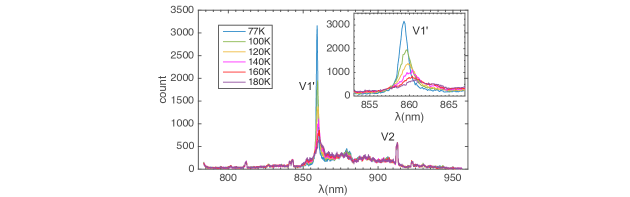
7 V emission spectra from SiC SCHBAR
Similar to diamond, 4H-SiC substrate has high quality mechanical property and is a host to divacancy (V-V) centers and silicon vacancy (V) centers, both of which contain electron spin with long coherence time4, 5. We experimentally probe the defect emission spectra of the SiC SCHBAR at the near infrared range (800-950 nm) where zero-phonon lines of V centers are located. In a home-built confocal microscope setup, we off-resonantly excite the defects with a 780 nm pump laser at 0.6 mW. The emission of the V centers is filtered by a long pass filter (cutoff wavelength at 800 nm) and then analysed with a spectrometer. We identify both V1 and V2 type of V centers in the recorded spectra (Fig. 11).
8 Pulse sequence for mechanical spin driving
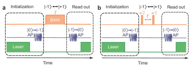
The implemented mechanical spin driving scheme is illustrated in Fig. 12(a). We first initialize the NV centers into state via optical polarization. Next, we use an adiabatic passage (AP) pulse to shelve the spins into state. We pulse on the acoustic wave for a period of time, , to induce spin population transfer between , states. After that, another AP pulse shuttles the residual spin population back to state, which is then read out optically. The sequence is repeated 80,000x for a single measurement. In ODMSR experiment, we fix 3 s, microwave power applied to transducer at 0 dbm, and take measurements as a function of external magnetic field. In mechanically-driven Rabi oscillation experiments, we repeat the sequence and measure time evolution of the spin population as we vary the pulse duration of the acoustic wave. The mechanical Ramsey coherence measurement is implemented in a similar way (Fig. 12(b)), where two mechanical pulses with varying time delay, , are used. For the measurement in the main text, =197 ns. We further introduce a phase shift to the second -pulse by , where is the equatorial rotating frequency of the spin in the Bloch sphere. This extra phase shift introduces a known periodicity to the measurement that aids visualization of the decay envelope. Similar protocols have been described in ref.41.
The contrast of the recorded , qubit Rabi oscillation is around 40% of that for a magnetically driven , qubit. We attribute this to the fact that the acoustic standing wave inside the resonator is spatially inhomogeneous, with a periodical anti-node every half wavelength, m. The depth resolution of our objective is m inside diamond. The resolution is improved deep inside the SIL to be m. In the acoustic spin driving measurement, the probed volume includes both high strain (anti-node) and un-strained (node) area. Considering that the acoustically-driven Rabi oscillation rate and the contrast scales proportionally with the strain amplitude, the acquired signal is an ensemble average over the Rabi oscillations across both a node and an anti-node of the acoustic mode, leading to a reduced contrast in measurement.
9 Strain evaluation
In the fabricated diamond SCHBAR device, stress and strain () generated from the transducer are primarily perpendicular to the (001) cut face of the diamond crystal. We define the crystal basis as X: [-110] Y:[001] Z:[110]. After taking into account the Poisson ratio, , the strain tensor can be written as,
| (6) |
Transforming into N-V axis, for example, , we have
| (7) |
The effective coupling to an NV center spin is then GHz, GHz11. The observed (2)2.19(14) MHz/Vp mechanically driven spin Rabi oscillation therefore corresponds to 1.59(14) V in strain.
The impedance of the micro-sized transducer is around 500 at 3 GHz. To suppress power reflections from the impedance mismatch, we engineer the length of the RF transmission line on the circuit board to act as a transformer. The actual voltage applied at the transducer is close to twice the voltage of that in a 50 matched network. We note that the electrical power and voltage reported in the main text are quoted for a 50 impedance matched load. The actual power applied to the transducer is less. Therefore, the power-to-strain efficiency of the device can be improved further using an impedance matching network.
10 Potential quantum applications
Even though the single spin-phonon cooperativity of the current device is low even at low temperature ( mK), , where Hz is the single spin-phonon coupling rate from zero-point motion of resonator (note that this is higher than HBAR devices made in the past14), is the coherence time of an NV center spin, is the resonator damping rate, is the phonon occupation number at temperature . The ensemble spin-phonon coupling is enhanced relative to the single spin-phonon coupling by , where is the number of coupled NV centers. For a dense ensemble of NV centers with density cm-350, there are close to addressable NV centers in a volume resonator. The effective spin-phonon coupling is kHz. The coupling can be further increased by considering alternative defect centers with stronger intrinsic spin-phonon coupling, i.e., SiV centers in diamond have been shown to have single spin-phonon coupling 100 THz/strain48, around 5000 times larger than that for an NV center. A diamond SCHBAR with SiV centers at a moderate density of cm-3 has ensemble spin-phonon coupling up to 1 MHz. Such high coupling can introduce a splitting in the resonator spectrum, which is detectable for a high quality resonator (, kHz). When the resonator and the SiV center spin transition frequencies are detuned, the frequency pull of the resonator due to coupling to SiV ensemble can be used for dispersive read-out47 of spin state and for spin manipulation of the resonator state.
References
- Awschalom et al. 2018 Awschalom, D. D.; Hanson, R.; Wrachtrup, J.; Zhou, B. B. Nature Photonics 2018, 12, 516
- Doherty et al. 2013 Doherty, M. W.; Manson, N. B.; Delaney, P.; Jelezko, F.; Wrachtrup, J.; Hollenberg, L. C. Physics Reports 2013, 528, 1–45
- Sukachev et al. 2017 Sukachev, D. D.; Sipahigil, A.; Nguyen, C. T.; Bhaskar, M. K.; Evans, R. E.; Jelezko, F.; Lukin, M. D. Physical review letters 2017, 119, 223602
- Christle et al. 2015 Christle, D. J.; Falk, A. L.; Andrich, P.; Klimov, P. V.; Hassan, J. U.; Son, N. T.; Janzén, E.; Ohshima, T.; Awschalom, D. D. Nature materials 2015, 14, 160
- Widmann et al. 2015 Widmann, M. et al. Nature materials 2015, 14, 164
- Ajoy and Cappellaro 2012 Ajoy, A.; Cappellaro, P. Physical Review A 2012, 86, 062104
- Ledbetter et al. 2012 Ledbetter, M.; Jensen, K.; Fischer, R.; Jarmola, A.; Budker, D. Physical Review A 2012, 86, 052116
- Bernien et al. 2013 Bernien, H.; Hensen, B.; Pfaff, W.; Koolstra, G.; Blok, M.; Robledo, L.; Taminiau, T.; Markham, M.; Twitchen, D.; Childress, L.; Hanson, R. Nature 2013, 497, 86
- Kalb et al. 2017 Kalb, N.; Reiserer, A. A.; Humphreys, P. C.; Bakermans, J. J.; Kamerling, S. J.; Nickerson, N. H.; Benjamin, S. C.; Twitchen, D. J.; Markham, M.; Hanson, R. Science 2017, 356, 928–932
- O’Connell et al. 2010 O’Connell, A. D.; Hofheinz, M.; Ansmann, M.; Bialczak, R. C.; Lenander, M.; Lucero, E.; Neeley, M.; Sank, D.; Wang, H.; Weides, M.; Wenner, J.; Martinis, J. M.; Cleland, A. N. Nature 2010, 464, 697
- Ovartchaiyapong et al. 2014 Ovartchaiyapong, P.; Lee, K. W.; Myers, B. A.; Jayich, A. C. B. Nature communications 2014, 5, 4429
- Burek et al. 2016 Burek, M. J.; Cohen, J. D.; Meenehan, S. M.; El-Sawah, N.; Chia, C.; Ruelle, T.; Meesala, S.; Rochman, J.; Atikian, H. A.; Markham, M.; Twitchen, D. J.; Lukin, M. D.; Painter, O.; Lonar, M. Optica 2016, 3, 1404–1411
- Cady et al. 2019 Cady, J.; Michel, O.; Lee, K.; Patel, R.; Sarabalis, C. J.; Safavi-Naeini, A. H.; Jayich, A. B. Quantum Science and Technology 2019,
- MacQuarrie et al. 2013 MacQuarrie, E.; Gosavi, T.; Jungwirth, N.; Bhave, S.; Fuchs, G. Physical review letters 2013, 111, 227602
- Golter et al. 2016 Golter, D. A.; Oo, T.; Amezcua, M.; Stewart, K. A.; Wang, H. Physical review letters 2016, 116, 143602
- Chen et al. 2018 Chen, H. Y.; MacQuarrie, E.; Fuchs, G. D. Physical review letters 2018, 120, 167401
- Whiteley et al. 2019 Whiteley, S. J.; Wolfowicz, G.; Anderson, C. P.; Bourassa, A.; Ma, H.; Ye, M.; Koolstra, G.; Satzinger, K. J.; Holt, M. V.; Heremans, F. J.; Cleland, A. N.; Schuster, D. I.; Galli, G.; D.Awschalom, D. Nat. Phys. 2019, 15, 490–495
- Chu et al. 2017 Chu, Y.; Kharel, P.; Renninger, W. H.; Burkhart, L. D.; Frunzio, L.; Rakich, P. T.; Schoelkopf, R. J. Science 2017, 358, 199–202
- Aigner 2008 Aigner, R. SAW and BAW technologies for RF filter applications: A review of the relative strengths and weaknesses. 2008 IEEE Ultrasonics Symposium. 2008; pp 582–589
- Bhugra and Piazza 2017 Bhugra, H.; Piazza, G. Piezoelectric MEMS resonators; Springer, 2017
- Baron et al. 2013 Baron, T.; Lebrasseur, E.; Bassignot, F.; Martin, G.; Pétrini, V.; Ballandras, S. Modeling and Measurement Methods for Acoustic Waves and for Acoustic Microdevices; InTechOpen, 2013
- Siegman 1986 Siegman, A. Lasers Oxford University Press; 1986
- Fang et al. 1989 Fang, S. R.; Zhang, S.; Lu, Z. F. IEEE transactions on ultrasonics, ferroelectrics, and frequency control 1989, 36, 178–184
- Shilton et al. 2008 Shilton, R.; Tan, M. K.; Yeo, L. Y.; Friend, J. R. J. Appl. Phys. 2008, 104, 014910
- Galliou et al. 2013 Galliou, S.; Goryachev, M.; Bourquin, R.; Abbé, P.; Aubry, J. P.; Tobar, M. E. Scientific reports 2013, 3, 2132
- Kharel et al. 2018 Kharel, P.; Chu, Y.; Power, M.; Renninger, W. H.; Schoelkopf, R. J.; Rakich, P. T. APL Photonics 2018, 3, 066101
- Hadden et al. 2010 Hadden, J.; Harrison, J.; Stanley-Clarke, A.; Marseglia, L.; Ho, Y.-L.; Patton, B.; O’Brien, J.; Rarity, J. Applied Physics Letters 2010, 97, 241901
- Yu et al. 2018 Yu, P.-L.; Opondo, N.; Dai, S.; Jiang, B.; Morisette, D. T.; Bhave, S. A. Single Crystalline 4H-SiC Membrane Resonators. 2018 IEEE International Frequency Control Symposium (IFCS). 2018; pp 1–5
- Lee et al. 2008 Lee, C.; Gu, E.; Dawson, M.; Friel, I.; Scarsbrook, G. Diamond and Related Materials 2008, 17, 1292–1296
- Friel et al. 2009 Friel, I.; Clewes, S.; Dhillon, H.; Perkins, N.; Twitchen, D.; Scarsbrook, G. Diamond and Related Materials 2009, 18, 808–815
- Appel et al. 2016 Appel, P.; Neu, E.; Ganzhorn, M.; Barfuss, A.; Batzer, M.; Gratz, M.; Tschöpe, A.; Maletinsky, P. Review of Scientific Instruments 2016, 87, 063703
- Ruf et al. 2019 Ruf, M.; IJspeert, M.; van Dam, S.; de Jong, N.; van den Berg, H.; Evers, G.; Hanson, R. Nano letters 2019,
- Bayn et al. 2011 Bayn, I.; Bolker, A.; Cytermann, C.; Meyler, B.; Richter, V.; Salzman, J.; Kalish, R. Applied Physics Letters 2011, 99, 183109
- Larson et al. 2000 Larson, J. D.; Bradley, P. D.; Wartenberg, S.; Ruby, R. C. Modified Butterworth-Van Dyke circuit for FBAR resonators and automated measurement system. 2000 IEEE Ultrasonics Symposium. Proceedings. An International Symposium (Cat. No. 00CH37121). 2000; pp 863–868
- Zener 1937 Zener, C. Physical review 1937, 52, 230
- Landau and Rumer 1937 Landau, L.; Rumer, G. Phys. Z. Sowjetunion 1937, 11
- Akhieser 1939 Akhieser, A. J. Phys.(Ussr) 1939, 1, 277
- Woodruff and Ehrenreich 1961 Woodruff, T.; Ehrenreich, H. Physical Review 1961, 123, 1553
- Landau 1986 Landau, L. D. Theory of elasticity; 1986
- Lifshitz and Roukes 2000 Lifshitz, R.; Roukes, M. L. Physical review B 2000, 61, 5600
- MacQuarrie et al. 2015 MacQuarrie, E.; Gosavi, T.; Moehle, A.; Jungwirth, N.; Bhave, S.; Fuchs, G. Optica 2015, 2, 233–238
- Jacques et al. 2009 Jacques, V.; Neumann, P.; Beck, J.; Markham, M.; Twitchen, D.; Meijer, J.; Kaiser, F.; Balasubramanian, G.; Jelezko, F.; Wrachtrup, J. Physical review letters 2009, 102, 057403
- Teissier et al. 2014 Teissier, J.; Barfuss, A.; Appel, P.; Neu, E.; Maletinsky, P. Physical review letters 2014, 113, 020503
- MacQuarrie et al. 2015 MacQuarrie, E.; Gosavi, T.; Bhave, S.; Fuchs, G. Physical Review B 2015, 92, 224419
- Barfuss et al. 2015 Barfuss, A.; Teissier, J.; Neu, E.; Nunnenkamp, A.; Maletinsky, P. Nature Physics 2015, 11, 820
- Taylor et al. 2008 Taylor, J.; Cappellaro, P.; Childress, L.; Jiang, L.; Budker, D.; Hemmer, P.; Yacoby, A.; Walsworth, R.; Lukin, M. Nature Physics 2008, 4, 810
- Blais et al. 2004 Blais, A.; Huang, R.-S.; Wallraff, A.; Girvin, S. M.; Schoelkopf, R. J. Physical Review A 2004, 69, 062320
- Meesala et al. 2018 Meesala, S. et al. Physical Review B 2018, 97, 205444
- Maris 1971 Maris, H. J. Physical Acoustics; Elsevier, 1971; Vol. 8; pp 279–345
- Choi et al. 2017 Choi, J.; Choi, S.; Kucsko, G.; Maurer, P. C.; Shields, B. J.; Sumiya, H.; Onoda, S.; Isoya, J.; Demler, E.; Jelezko, F.; Yao, N. Y.; Lukin, M. D. Physical review letters 2017, 118, 093601