Extending the Near-infrared Band-edge Absorption Spectrum of Silicon by Proximity to a 2D Semiconductor
Abstract
Because of its low-cost, silicon is the standard material for photovoltaic conversion. Yet, its band-edge absorption spectrum is narrower than the spectrum of the solar radiation, which reduces its conversion efficiency. In this paper, it is shown that the spectrum of absorbance of silicon can be extended to longer wavelengths by proximity to a two-dimensional (2D) semiconductor. Photo-induced Hall effect, together with standard absorption spectroscopy, was employed to estimate the increase of efficiency of absorbance of a 2D-platinum-diselenide/intrinsic-silicon bilayer. The bilayer shows a significantly higher absorption in the infrared as compared to the single films. Moreover, an overall increase of absorption efficiency by a factor twenty was measured in the entire spectrum of light of a halogen lamp. X-ray Photoelectron Spectroscopy (XPS) confirms that a reduction of the band-gap occurs in the silicon substrate at the interface between the two semiconductors. The results are interpreted in the framework of band-gap narrowing due to hole-plasma confinement in the Si, induced by electron-confinement in the 2D film. Possible application of the effect in photo-voltaic cells is discussed.
Keywords: 2D semiconductors, photo-conversion, band-gap engineering
1 Introduction
The need for inexpensive renewable energy sources and the potentialities of harvesting the huge energy amount coming from the sun in a more efficient way, has been pushing both industry and research of last decades towards finding new solutions to increase the solar cells efficiency.
Among the large variety of materials exploited in photovoltaics, silicon remains the most used one because of its abundance and its consequently very low-cost. Nevertheless, its band-gap of 1.12 eV represents one of the major issues limiting its performances in photovoltaic conversion [1, 2]. It sets the edge of the absorption spectrum at about 1107 nm [3]. As a consequence, the largest amount of the near-infrared solar spectrum content is lost and does not take part to the energy conversion process. Different solutions have been proposed in literature to enhance the absorption of the infrared light. The possibility of coupling more semiconductors in multi-gap [4], or multi-junction [5], tandem solar cells is an example. In particular, two or more solar cells with different absorption characteristics are series-connected together thorough tunnel junctions with the aim of covering a wider part of the solar spectrum. Recent examples of tandem solar cells make use of polymers [6] and organic cells [7].
In the same direction goes the exploitation of thin films to improve the infrared absorption [8]. First examples are given in refs. [9, 10] where a CuInGaSe2 and a low band-gap polymer were proposed, respectively. More recently, the usage of quantum dots [11, 12] and nanowires [13, 14] was proposed for infrared photovoltaics.
After graphene was discovered in 2004 [15], new possibilities arose in developing photovoltaic devices [16, 17], leading also to the usage of other two-dimensional (2D) materials [18]. Among the latter class of semiconductors, most promising for infrared absorption and detection seem to be the transition metal dichalcogenides (TMDs) [19, 20, 21, 22, 23].
In this paper, a simple method to extend the near-infrared band-edge absorption spectrum of silicon (Si) is presented. In particular, 2D platinim diselenide (PtSe2), a narrow band-gap TMD semiconductor, is exploited. As explained in the following, the large difference in band-gap between the two semiconductors results in an electron confinement in the 2D layer, which induces a hole-plasma in the Si. The concentration of holes decays as the inverse of the distance from the interface, resulting in a gradual narrowing of the band-gap and, therefore an increase in both the absorbance efficiency and absorbance spectrum. The high resistivity of the intrinsic silicon favours the confinement of the hole-plasma near the interface. Photo-induced Hall effect [24], together with standard spectroscopy, allowed us to estimate the increase of photo-conversion efficiency without having to resort to electrical measurements, which would require the use of doped semiconductors. The bilayer behaves as a single, engineered semiconductor with an overall increase of 20 times in absorbance, partially due to an increase of absorbance in the infrared range, which takes place near the interface in the Si, not in the 2D semiconductor. Our interpretation is supported by angle-resolved X-ray Photoelectron Spectroscopy (XPS) measurements, which confirm that a reduction of the band-gap exists in the Si near the interface.
2 Results
The two-dimensional semiconductor used in the present work is a two/three atomic layer platinum diselenide (PtSe2) with 1.8 nm thickness. It is a transition metal dichalcogenide which has been demonstrated to undergo a transition from metal to semiconductor by reducing its thickness from bulk to two-dimensional layers [25]. The system of interest here is an cm2 PtSe2/Si bilayer, where the Si substrate was chosen to be intrinsic Si (i-Si) for reasons that will be explained in the following. An cm2 PtSe-Al2O3 bilayer was used as reference in optical measurements, while two more reference samples, namely Pt/PtSe2/-Al2O3 and Pt/Si, were used as reference for photo-induced Hall measurements.
2.1 Raman Spectroscopy
The measured Raman spectrum of the 2D film is shown in Figure 1. The measurement was carried out on the PtSe-Al2O3 sample, in order to avoid the high intensity signal from the Si. The spectrum is consistent with the one expected for the 2D semiconductor [26].
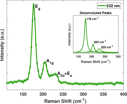
In particular, two main peaks at 176 cm-1 and 205 cm-1 and one with lower intensity at 229 cm-1 can be observed. The first two are assigned to Eg and A1g modes, respectively. The third one corresponds to the overlapping of A2u and Eu modes. As discussed in ref. [26] the latter peak disappears for thickness of about 5 nm. Furthermore, the higher its relative intensity, with respect to the more prominent ones, the thinner the PtSe2 layer. As a consequence, the Raman spectrum in Figure 1 confirms the two-dimensional nature of the PtSe2 layer under test.
2.2 Fourier Transform Infrared Spectroscopy
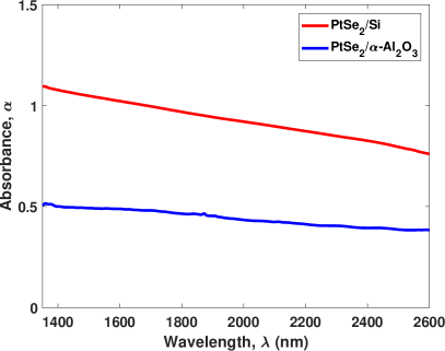
In order to investigate how the proximity to the 2D semiconductor affects the optical behavior of the silicon substrate, Fourier Transform Infrared (FTIR) spectroscopy measurements were performed on the two samples. Since the bandgap of Si is eV, corresponding to a cut-off absorption wavelength of nm, Si is expected to be completely transparent in the infrared. On the contrary, in Figure 2 one can see that a significant absorbance exists in the near-infrared, beyond 1107 nm in the PtSe2/Si sample. The absorbance is not negligible up to 6000 nm, as shown in the full absorbance spectrum in Figure S1 (see Supporting Information). The same measurement carried out on the PtSe-Al2O3 reference sample shows that the absorbance in the 2D film in the near-infrared is lower with respect to the first sample. The increase of absorbance in the reference sample for wavelengths longer than 5000 nm (see Figure S1, Supporting Information) can be ascribed to the absorbance of the sapphire substrate [27, 28], and is of no interest in the present framework.
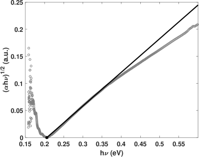
The band-gap of the 2D semiconductor was estimated through the Tauc analysis [29] of the absorbance spectrum of the PtSe-Al2O3 reference sample. The Tauc plot of the absorbance spectrum is shown in Figure 3. The noise at low photon energies is due to the aforementioned absorbance of the sapphire for wavelengths longer than 5000 nm. Then, a clear change of slope is observed for photon energies near the expected band-gap value. The absorbance depends on the difference between photon energy and band-gap, as , where for indirect band-gap semiconductors [30], such as in the case of 2D PtSe2 [31]. As a consequence, a bandgap eV was estimated by using the intercept to the axis (see Figure 3). This value is in agreement with ref. [32], in which a band-gap of 0.21 eV was reported for monolayer PtSe2.
2.3 Photo-induced Hall effect measurements
Photo-induced Hall effect [24] offers the possibility to characterize the optical behavior of a semiconductor without flowing of a net-charge current. As will be discussed in the next section, this is important to exclude band-gap narrowing due to excitation and injection of high-density carriers through the 2D/Si interface [33]. The working principle is briefly explained in the following with the help of Figure 4. A metal with high work-function, such as platinum (Pt) is deposited on the semiconductor or, in this case, on the semiconductor hetero-structure. The thickness of the metal is chosen in such a way that light can penetrate without significant attenuation for wavelengths as long as infrared radiations. In this experiment the thickness of the Pt was 3 nm. The metal forms a Schottky barrier to the semiconductor. As photons are converted into electron-hole pairs, while holes can easily be neutralized by electrons in the metal, electrons are confined near the interface, if the semiconductor is highly resistive. This results in a rounding-off of the barrier due to image force effect [34]. The reduction of the barrier potential allows electron to be injected into the metal, as schematically shown in Figure 4a. If a magnetic field is applied in the sample plane, an open-circuit voltage appears that is transverse to the metal (Figure 4b). At equilibrium, the current of the holes and the current of the electrons are equal and no net-current flows, while the current densities are not uniform because of the Lorentz’s forces exerted on the carriers.
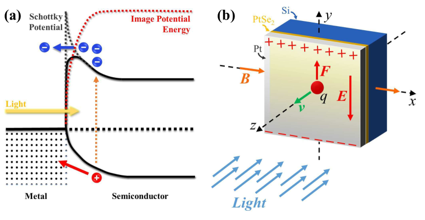
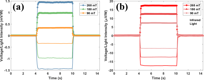
Figure 5a shows the open-circuit voltage detected on the Pt/PtSe2/Si when illuminated by a halogen lamp and for different values of the applied magnetic field. Figure 5b shows the same measurement when a long-pass, infrared filter with cut-off wavelength of 1250 nm (which is safely longer than 1107, the absorption spectrum of silicon), is placed in front of the sample. In both cases, the Hall voltage was normalized to the measured light intensity. One can clearly see that photo-conversion occurs in the near-infrared, in agreement with the FTIR measurements.
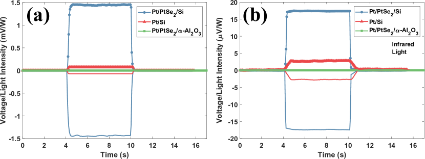
In order to understand where absorption of infrared occurs we prepared two additional reference samples, Pt/PtSe2/-Al2O3 and Pt/Si for photo-induced Hall effect. In Figure 6a and Figure 6b we compare the photo-induced Hall effect measured on the three samples at a fixed value of the magnetic field. In agreement with the FTIR measurements, absorption of infrared light is highly enhanced in the Pt/PtSe2/Si bilayer as compared to the case of single semiconductors.
Finally, photo-induced Hall measurements with daylight blue and red filters were carried out and shown in Figure S2 (see Supporting Information). By comparing the relative intensities of the signals obtained over the two samples, it is straightforward to note that a shift in the absorbance peak to longer wavelengths is obtained in the Pt/PtSe2/Si sample with respect to the Pt/Si one. This demonstrates that the 20 times increase of the overall absorbance mainly occurs in the red and infrared wavelength range.
2.4 X-ray Photoelectron Spectroscopy
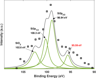
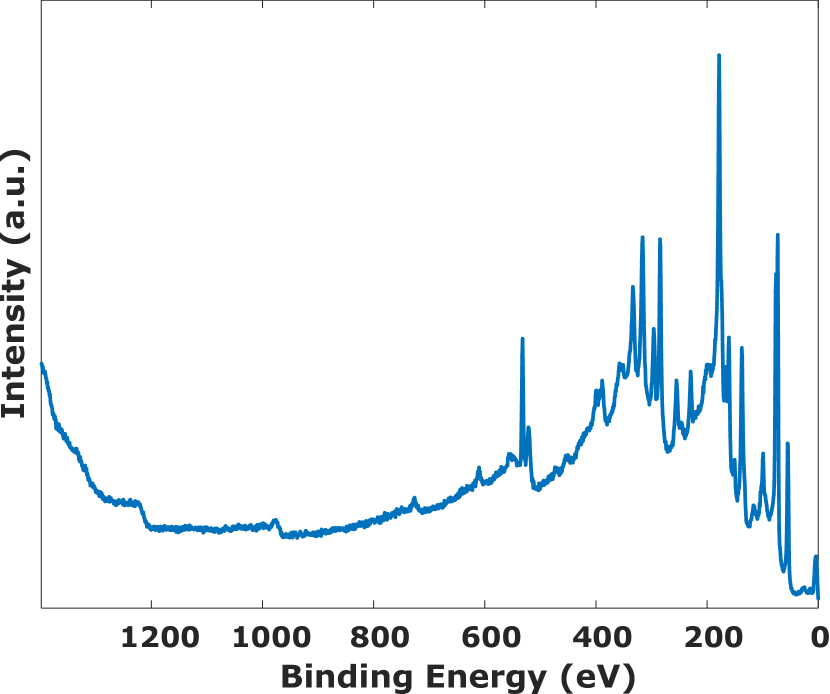
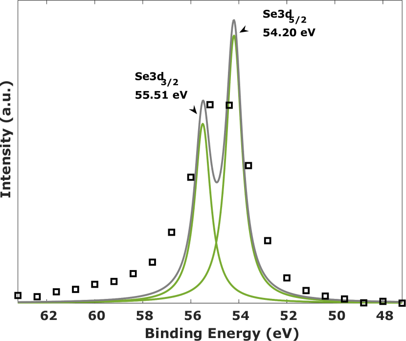
X-ray Photoelectron Spectroscopy (XPS) measurements were carried out on the PtSe2/Si sample. The angle of the beam with respect to the sample was changed until the peaks of the Si under the 2D film could be resolved. The full spectrum is shown in Figure S3 (see Supporting Information). The Si peaks are shown in Figure 7. One can clearly observe the presence of four peaks that are better resolved by Lorentzian deconvolution. The two peaks at 98.94 eV and 100.3 eV are the expected 2p3/2 and 2p1/2 peaks of Si [35]. The peak at higher binding energy 102.6 eV can be attributed to residues of SiO2 [36] due to the transfer process of the 2D material on the silicon substrate (see Materials and Methods). Surprisingly, a forth peak can be resolved at lower binding energies, at around 95.59 eV. As discussed in the following section, this peak suggests a narrowing of the Si band-gap near the interface.
3 Discussion
The results presented in the previous section suggest a profound change of the band-structure of the Si near the interface on a mesoscopic scale. In particular, they suggest a band-gap narrowing (BGN), which results in both an increase of the absorption efficiency in the visible range and an extension of the absorption spectrum into the near infrared. A BGN of the order of hundreds of mV in Si can only be ascribed to the presence of an electron-hole plasma [37]. In brief, the band-gap is by definition the minimum energy required to generate an unbound electron-hole pair. The distance between the electron and the hole in the crystal is such that electrostatic attraction between the two particles can be neglected. On the contrary, excitons in a crystal can be excited by providing smaller energy. An exciton is a quasiparticle in which an electron and a hole are attracted to each other by the electrostatic Coulomb force. The existence of a plasma favours conversion of photons into excitons. This requires less energy than that required to generate an unbound electron-hole pair. A reduction of the energy that a photon must possess to excite an electron-hole pair is equivalent to a reduction of the band-gap.
The plasma can have three possible origins: i) heavy doping; ii) optical excitation of a large concentration of electron-hole pairs, usually through laser sources and iii) injection of high-density carriers through the interface of a biased junction, in which case the plasma, and therefore the BGN, is confined near the interface. Heavy doping in silicon has indeed been proven effective to extend its spectrum of absorption to the infrared [38, 39]. Of course, this possibility can here be excluded because the silicon used in this work is intrinsic. Excitation of a large concentration of electron-hole pairs can also be excluded, because in our experiment, unlike the Pt/PtSe2/Si sample, the Pt/Si sample does not absorb infrared light, under the same experimental conditions.
Last, injection of high-density carriers through the interface can be ruled out because the FTIR in Figure 2 shows that a BGN of the bilayer exists under no electrical bias. Besides, in photo-induced Hall effect, no net-current flows through the hetero-junction. One must conclude that in our system the existence of a plasma confined near the interface in the Si must be due to the proximity to the 2D film.
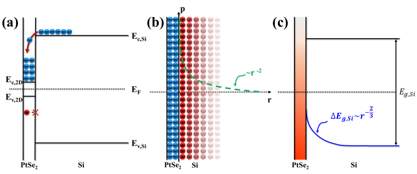
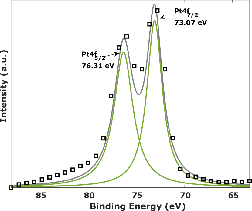
As the Si substrate is placed in intimate contact with the 2D semiconductor, electrons in the conduction band (CB) of the Si see a large density of energy states available across the interface and migrate (see Figure 8a). On the contrary, holes from the 2D film see a large potential barrier and cannot migrate into the Si. The 2D behaves as a potential well for the electrons. As electrons are confined in a two/three atomic layers thick film, Coulomb interaction is not negligible. On one side, confinement of electrons in a 2D semiconductor is well known to induce a change in the band-structure of the 2D [40], which we shall not discuss further here because the effect we observe is in the bulk semiconductor. From simple electrostatic considerations, an electron plasma confined in the 2D must induce a hole plasma in the Si, in which the charge density decays as , where is the distance from the interface (see Figure 8b). The BGN is known to increases as [41]. Therefore, (see Figure 8c), where the singularity in is due to the fact that the discrete nature of matter has not been taken into account. As a hole-plasma exists in the Si, near the interface, an upward bending of the valence band (VB) is at the origin of the BGN. This scenario is supported by the XPS spectrum shown in Figure 7. In this measurement, the low energy peak at 95.59 eV can not be assigned to SiO2 nor to Pt and Se in the 2D semiconductor. Peaks related to the latter two elements are located at much lower binding energies and are shown in Figure S4 and Figure S5 (see Supporting Information), respectively. As a consequence, the peak at 95.59 eV indicates that a reduction of the band-gap occurs in the Si substrate near the interface with the 2D layer. This BGN can be regarded as a 2D/semiconductor version of the rounding-off of the CB edge in metal/semiconductor Schottky junctions due to confinement of electrons in the semiconductor near the interface (see Figure 4a and Figure 8c). Except, in 2D/semiconductor bilayers, electrons are confined in the 2D, which results into a bending of the VB, rather than the CB.
It is interesting to notice that a similar bending of the valence band of a bulk semiconductor in proximity to a 2D layer was recently reported in ref. [42] and ascribed to electron confinement, although in the cited work only an electrical characterization of the bilayer was carried out and therefore no evidence of BGN was reported.
Let us also point out that the effect we here observe should not be confused with the proximity effect due the penetration of
electronic wavefunctions of one semiconductor into the other, which is purely quantum-mechanical and completely negligible in semiconductors.
Finally, let us speculate on how this effect could be employed in a photo-voltaic cell. If the intrinsic silicon substrate were to be replaced by doped Si to work as the active layer of a photo-voltaic cell, we predict the BGN to decrease as the doping level increases. This is because the hole-plasma would not be confined near the interface, as charge could easily diffuse trough the bulk semiconductor. A structure of the kind , where and represent a p-type and a highly doped n-type semiconductor, respectively, could yield a higher efficiency than a standard structure, if an appropriate choice of the thickness of the i-Si is made. The thickness should be large enough to allow confinement and small enough not to increase significantly the overall resistance of the multilayer.
4 Conclusion
A simple method to enhance the near-infrared absorption of intrinsic silicon was proposed and discussed in this paper. In particular, a 2D PtSe2/i-Si bilayer was studied. It was shown that electron confinement in the 2D layer induces an hole-plasma in the silicon substrate. As a consequence, an upward bending of the valence band in the bulk semiconductor is induced, leading to an overall narrowing of the band-gap near the interface, as confirmed by XPS measurements. Furthermore, photo-induced Hall effect showed that an increase of absorbance by up to 20 times can be induced in Si, partially due to an extension of the absorbance spectrum to the infrared. The possibility of using such a strategy in solar cells technology was preliminarily discussed, too, and will be the subject of future works.
5 Materials and Methods
PtSe2 samples films were purchased from SixCarbon Technology (Shenzhen). The average thickens of the layer, as measured by atomic force microscopy (AFM), was 1.8 nm. The 2D layers were grown on SiO2 substrates and then transferred on the specific substrate (Si or -Al2O3) and annealed in vacuum at C. The Raman spectrum in Figure 1 was measured with a WITec ALPHA300 (laser at 532 nm). A PerkinElmer spectrometer was used to acquire the Fourier-transform infrared spectra shown in Figure 2. Pt thin films for photo-induced Hall effect measurements were deposited thorough Pulsed Laser Deposition (PLD) method (laser energy: 300 mJ, frequency: 3 Hz , pulse width: 25 ns, deposition time: 180 s, pressure: Torr). Magnetic fields were applied through an GMW 5403 electromagnet supplied by two RS-PRO RSPD 3303C. A halogen lamp Halopar 30 by Osram was used as the light source and an FELH1250 edge-pass filter (long-pass wavelength at 1250 nm) by ThorLabs was exploited to cut the visible part. The open-circuit Hall voltage was measured by using a Keithley 2182A nanovoltmeter. Electric contacts to the samples were made by aluminum wire bondings.
Supporting Information
Supporting Information is available after the references.
Acknowledgements
This study was funded by the Science, Technology and Innovation Commission of Shenzhen Municipality (Project no. JCYJ20170307091130687).
References
References
- [1] Tiedje T, Yablonovitch E, Cody G D and Brooks B G 1984 IEEE Trans. Electron Devices 31 711–716
- [2] Richter A, Hermle M and Glunz S W 2013 IEEE J. Photovolt. 3 1184–1191
- [3] Shalav A, Richards B, Trupke T, Krämer K and Güdel H U 2005 Appl. Phys. Lett. 86 013505
- [4] Marti A and Araújo G L 1996 Sol. Energy Mater. Sol. Cells 43 203–222
- [5] Tobias I and Luque A 2002 Progress in Photovoltaics: Research and Applications 10 323–329
- [6] You J, Dou L, Yoshimura K, Kato T, Ohya K, Moriarty T, Emery K, Chen C C, Gao J, Li G et al. 2013 Nat. Commun. 4 1446
- [7] Meng L, Zhang Y, Wan X, Li C, Zhang X, Wang Y, Ke X, Xiao Z, Ding L, Xia R et al. 2018 Science 361 1094–1098
- [8] Lee T D and Ebong A U 2017 Renewable Sustainable Energy Rev. 70 1286–1297
- [9] Devaney W, Chen W, Stewart J and Mickelsen R 1990 IEEE Trans. Electron Devices 37 428–433
- [10] Brabec C J, Winder C, Sariciftci N S, Hummelen J C, Dhanabalan A, van Hal P A and Janssen R A 2002 Adv. Funct. Mater. 12 709–712
- [11] Yan X, Cui X, Li B and Li L s 2010 Nano Lett. 10 1869–1873
- [12] Tang J and Sargent E H 2011 Adv. Mater. 23 12–29
- [13] Lin C and Povinelli M L 2009 Opt. Express 17 19371–19381
- [14] Kelzenberg M D, Boettcher S W, Petykiewicz J A, Turner-Evans D B, Putnam M C, Warren E L, Spurgeon J M, Briggs R M, Lewis N S and Atwater H A 2010 Nat. Mater. 9 239
- [15] Novoselov K S, Geim A K, Morozov S V, Jiang D, Zhang Y, Dubonos S V, Grigorieva I V and Firsov A A 2004 Science 306 666–669
- [16] Liu Z, Liu Q, Huang Y, Ma Y, Yin S, Zhang X, Sun W and Chen Y 2008 Adv. Mater. 20 3924–3930
- [17] Chien C T, Hiralal P, Wang D Y, Huang I S, Chen C C, Chen C W and Amaratunga G A 2015 Small 11 2929–2937
- [18] Liu Z, Lau S P and Yan F 2015 Chem. Soc. Rev. 44 5638–5679
- [19] Wang Q H, Kalantar-Zadeh K, Kis A, Coleman J N and Strano M S 2012 Nat. Nanotechnol. 7 699
- [20] Bernardi M, Palummo M and Grossman J C 2013 Nano Lett. 13 3664–3670
- [21] Jariwala D, Sangwan V K, Lauhon L J, Marks T J and Hersam M C 2014 ACS Nano 8 1102–1120
- [22] Mak K F and Shan J 2016 Nat. Photonics 10 216
- [23] Tan C L and Mohseni H 2018 Nanophotonics 7 169–197
- [24] Li D and Ruotolo A 2018 Sci. Rep. 8 4372
- [25] Ciarrocchi A, Avsar A, Ovchinnikov D and Kis A 2018 Nat. Commun. 9 919
- [26] O’Brien M, McEvoy N, Motta C, Zheng J Y, Berner N C, Kotakoski J, Elibol K, Pennycook T J, Meyer J C, Yim C et al. 2016 2D Mater. 3 021004
- [27] Thomas M E, Joseph R I and Tropf W J 1988 Appl. Opt. 27 239–245
- [28] Druy M A, Elandjian L, Stevenson W A, Driver R D, Leskowitz G M and Curtiss L E 1990 Fourier transform infrared (ftir) fiber optic monitoring of composites during cure in an autoclave Fiber Optic Smart Structures and Skins II vol 1170 (International Society for Optics and Photonics) pp 150–160
- [29] Tauc J, Grigorovici R and Vancu A 1966 Phys. Status Solidi B 15 627–637
- [30] Viezbicke B D, Patel S, Davis B E and Birnie III D P 2015 Phys. Status Solidi B 252 1700–1710
- [31] Kandemir A, Akbali B, Kahraman Z, Badalov S, Ozcan M, İyikanat F and Sahin H 2018 Semicond. Sci. Technol. 33 085002
- [32] Wang Y, Li L, Yao W, Song S, Sun J, Pan J, Ren X, Li C, Okunishi E, Wang Y Q et al. 2015 Nano Lett. 15 4013–4018
- [33] del Alamo J A and Swanson R M 1987 Solid-State Electron. 30 1127–1136
- [34] Chang C and Sze S 1970 Solid-State Electron. 13 727–740
- [35] Cerofolini G, Galati C and Renna L 2003 Surf. Interface Anal. 35 968–973
- [36] Wagner C D, Riggs W M, Davis L E, Moulder J F and Muilenberg G E 1979 Handbook of X-ray photoelectron spectroscopy (Perkin-Elmer Corporation)
- [37] Persson C, Lindefelt U and Sernelius B 2000 Solid-State Electron. 44 471–476
- [38] Balkanski M, Aziza A and Amzallag E 1969 Phys. Status Solidi B 31 323–330
- [39] Schmid P 1981 Phys. Rev. B 23 5531
- [40] Alidoust N, Bian G, Xu S Y, Sankar R, Neupane M, Liu C, Belopolski I, Qu D X, Denlinger J D, Chou F C et al. 2014 Nat. Commun. 5 4673
- [41] Jain S and Roulston D 1991 Solid-State Electron. 34 453–465
- [42] Molle A, Lamperti A, Rotta D, Fanciulli M, Cinquanta E and Grazianetti C 2016 Adv. Mater. Interfaces 3 1500619
Supporting Information
Extending the Near-infrared Band-edge Absorption Spectrum of Silicon by Proximity to a 2D Semiconductor
Valerio Apicella, Teslim Ayinde Fasasi, Antonio Ruotolo*
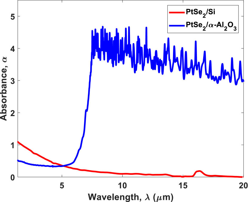
The jump in the PtSe2/-Al2O3 absorbance at 5000 nm is due to the sapphire substrate [1,2] and the signal becomes very noisy beyond such a wavelength. It is highlighted that the absorbance of infrared light in the PtSe2/Si is higher than that in the 2D film for wavelengths as long as 5000 nm, despite the fact that Si is completely transparent to infrared for 1107 nm.
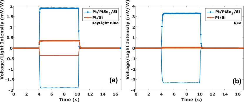
The light emitted by the halogen lamp was filtered in two different wavelength spectra. Two filters by Edmund Optics were used. The first one, namely a daylight blue filter, has cut-on and cut-off wavelengths at 340 and 465 nm, respectively. The second one, a red filter, has the cut-on wavelength at 600 nm. It is possible to observe that the peak of photo-induced Hall voltage shifts toward longer wavelengths when the 2D semiconductor exerts its proximity on the Si substrate.
-
-
The position of peaks for Pt and Se is in agreement with XPS measurements on PtSe2 reported in refs. [3,4].
References
M. E. Thomas, R. I. Joseph, W. J. Tropf, Applied Optics 1988, 27, 2 239.
M. A. Druy, L. Elandjian, W. A. Stevenson, R. D. Driver, G. M. Leskowitz, L. E. Curtiss, In Fiber Optic Smart Structures and Skins II, volume 1170. International Society for Optics and Photonics 1990 150-160.
C. Xie, L. Zeng, Z. Zhang, Y.-H. Tsang, L. Luo, J.-H. Lee, Nanoscale 2018, 10, 32 15285.
L.-H. Zeng, S.-H. Lin, Z.-J. Li, Z.-X. Zhang, T.-F. Zhang, C. Xie, C.-H. Mak, Y. Chai, S. P. Lau, L.-B. Luo, et al., Advanced Functional Materials 2018, 28, 16 1705970.