Defect-Moderated Oxidative Etching of MoS2
Abstract
We report a simple technique for the selective etching of bilayer and monolayer MoS2. In this work, chosen regions of MoS2 were activated for oxygen adsorption and reaction by the application of low doses of He+ at 30 keV in a gas ion microscope. Raman spectroscopy, optical microscopy and scanning electron microscopy were used to characterize both the etched features and the remaining material. It has been found that by using a pre-treatment to introduce defects, MoS2 can be etched very efficiently and with high region specificity by heating in air.
I Introduction
| Ref. | Synthesis | Layer No. | Etchant | Characterisation | Oxide | ||
|---|---|---|---|---|---|---|---|
| Wu et al. (2013) | Mech. Exf. | 1, 2, 4L | °C | - | Air | AFM MFM | MoO3 |
| Zhou et al. (2013) | Mech. Exf. | 1-4L | °C | - | Air | AFM Raman | None |
| Zhou et al. (2013) | Mech. Exf. | 10L+ | °C | - | Air | AFM Raman | None |
| Yamamoto et al. (2013a) | Mech. Exf. | 1-4L | °C | °C | Ar/O2 | AFM Raman | None |
| Yamamoto et al. (2013a) | Mech. Exf. | 40nm | °C | - | Ar/O2 | AFM Raman | MoO3 |
| Neupane et al. (2016) | CVD | 2-3L | °C | - | O2 | N/A | N/A |
| Rao et al. (2017) | CVD | Few, 3L | °C | - | Ar/O2 | Raman | None |
For 2D transition metal dichalcogenides (TMDs) to become prolific in devices, their stability in diverse chemical and physical environments must be understood and highly scalable processing must be available. MoS2 is one such material which exhibits diverse properties in its various forms Kam and Parkinson (1982); Mak et al. (2010); Lee et al. (2010); Splendiani et al. (2010); Liu et al. (2013), allowing potential applications in flexible electronics Pu et al. (2012), photodetectors Lopez-Sanchez et al. (2013) and solar cells Zhang et al. (2014). MoS2 synthesized by chemical vapor deposition (CVD) can be produced in relatively large crystals (several micrometers) with control over the density of defects and layer number Zhan et al. (2012); Lee et al. (2012); Song et al. (2015). However, sulfur vacancies are inevitable, even in high quality samples and a native n-type doping is typically noted Qiu et al. (2013); Fivaz and Mooser (1967). The oxidation of bulk or powdered MoS2 in air to MoOx has been well scrutinized because of profound impact on its performance as an industrial lubricant—transforming electronic, chemical, optical, and tribological properties Ballou and Ross (1953); Ross and Sussman (1955); Lansdown (1999). When heated in the presence of oxygen, the reaction forms MoO3 and SO2 molecules:
| (1) |
The temperature at which the reaction occurs is greatly determined by the condition of the material, reportedly ranging from 100°C for a powder Ross and Sussman (1955), to 400°C Khare and Burris (2013) for sputtered MoS2 coatings. The oxidative thinning and/or etching of 2D MoS2 can be achieved by heating in the presence of O2 to 240°C or higher Yamamoto et al. (2013a); Zhou et al. (2013); Wu et al. (2013); Gan et al. (2016); Neupane et al. (2016). Other oxidants have also been used such as the more reactive O3 Yamamoto et al. (2013b); Azcatl et al. (2014), XeF2 Huang et al. (2013) and oxygen containing plasmas Zhu et al. (2016); Jadwiszczak et al. (2017, 2019). Many reports demonstrate a mesh of quasi-equilateral triangular pits in the MoS2 surface after exposure to oxidizing conditions Wu et al. (2013); Zhou et al. (2013); Yamamoto et al. (2013a); Gan et al. (2016). These pits are likely bounded by the p-doped zig-zag-Mo edge, with each Mo atom bonded to two O atoms in a wide range of O chemical potentials Schweiger et al. (2002); Jaramillo et al. (2007); Zhou et al. (2013); Gan et al. (2016). At temperatures above 250°C, the density of etched pits depends on the availability of defect sites about which to nucleate. Pit density does not correlate strongly with the environmental conditions Yamamoto et al. (2013a, b). Furthermore, kinetic Raman spectroscopy and DFT studies suggest that the reaction energy for defective MoS2 is much lower than the value calculated for pristine material Rao et al. (2017); K. C. et al. (2015). The sublimation temperature for bulk MoO3 is normally about 700°C but that value can be substantially less for nanoscale MoO3 or MoOx as a reaction product Ross and Sussman (1955); Lince and Frantz (2000); Hu et al. (2015). In reports of bulk, thicker films (40 nm) and some powdered MoS2 the oxidized molybdenum remains and its relative content can be measured Ross and Sussman (1955); Lince and Frantz (2000); Yamamoto et al. (2013a). Wu et al. used magnetic force microscopy and atomic force microscopy to find evidence of MoO3 after heating few-layer MoS2 Wu et al. (2013). However, evidence for the presence of oxide material is mixed for thin samples (1-4L) and the precise conditions for oxidative experiments in which the MoOx reaction product sublimes or endures remain understudied Yamamoto et al. (2013a); Zhu et al. (2016). It seems that MoO3 sublimation dominates for some kinetic and material conditions (especially thin samples). Heating experiments and results from papers discussed here are summarized in table 1.
Raman spectroscopy has been employed extensively in the characterization of MoS2 in various forms such as bulk Wieting and Verble (1971); Chen and Wang (1974); Windom et al. (2011); Livneh and Spanier (2015), powder Stacy and Hodul (1985), nanoparticles Frey et al. (1999); Rice et al. (2013) and few-layer/monolayer Lee et al. (2010); Chakraborty et al. (2012); Li et al. (2012a, b); Zhao et al. (2013). The high-energy optical modes that are Raman active in monolayer/bilayer MoS2 are the following: the / peak at 385 cm-1 which arises from the intralayer, in-plane motion of Mo and S atoms with respect to each other and the / peak at 405 cm-1 which arises from the intralayer, out-of-plane motion of S atoms Lee et al. (2010); Li et al. (2012a). The frequency and width of the / peak has been reported to be sensitive to electrostatic doping while the position, splitting and width of / peak is more sensitive to strain Chakraborty et al. (2012); Rice et al. (2013); McCreary et al. (2016). It has been shown using symmetry arguments, DFT calculations and experiments that an upshift in the frequency and decrease in the linewidth of the Raman / modes represent a strong electron interaction for that optical phonon. Electron density is significantly diminished by oxygen treatment above °C causing these effects on the / mode Chakraborty et al. (2012); Shi et al. (2013); Wu et al. (2013); Yamamoto et al. (2013a). Since etching/thinning of 2D MoS2 has not been found at temperatures of 200°C, narrowing and upshifting of the / modes at temperatures below °C are caused by increased adsorption rather than oxidation. Neupane et al. performed experiments with dry O2 gas on CVD MoS2 and demonstrated in Raman and photoluminescence spectroscopies that annealing in H2 caused a reversal of the effects of adsorbed oxygen on the doping state of the remaining material Neupane et al. (2016). The adsorption energy of molecular oxygen on the monolayer MoS2 surface is reduced by approximately half in the presence of a surface sulfur vacancy defect. Therefore, controlling defect density is critical in controlling the adsorption of oxygen and hence oxidation K. C. et al. (2015).
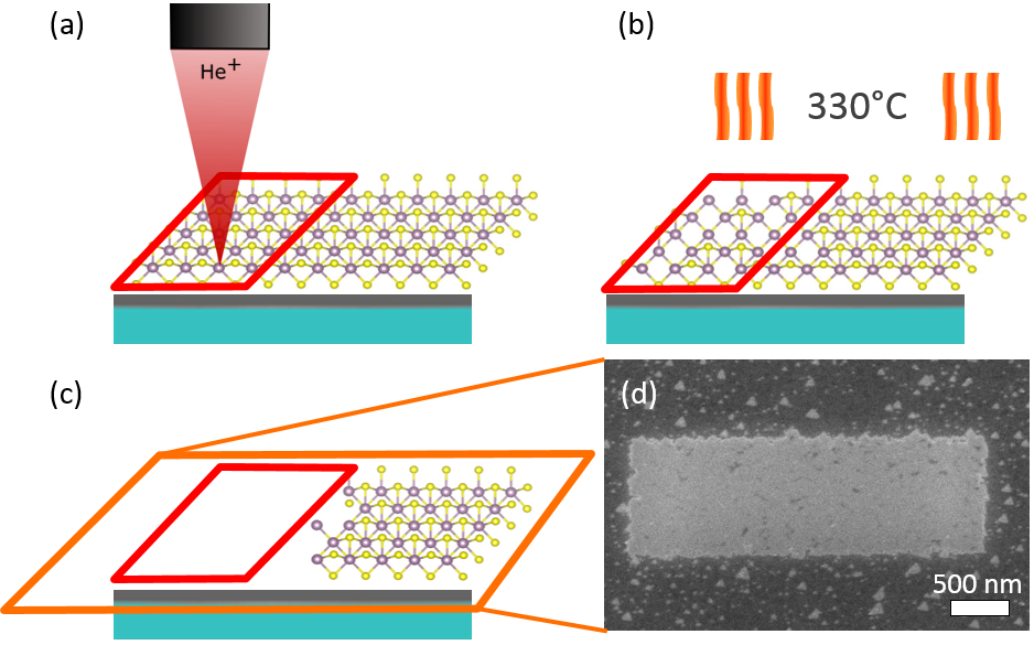
The precise defect-engineering of 2D materials has been demonstrated using highly spatially resolved ion irradiation in a helium ion microscope (HIM) Fox et al. (2015); Klein et al. (2018); Maguire et al. (2018a, b); Iberi et al. (2016); Stanford et al. (2016); Nanda et al. (2017); Zhou et al. (2016). In this paper, we use such methods to moderate adsorption and the oxidative reaction of MoS2 in air, demonstrating a high degree of spatial control over the oxidation reaction, as illustrated schematically in figure 1. This work facilitates high throughput patterning for preferential oxygen adsorption and oxidation. Our Raman spectroscopy results indicate that the selective adsorption of oxygen at defect sites could also be used to create a localized p-type doping environment. In this paper, unprecedented spatial control of the oxidation reaction by pre-treating with an ion beam is demonstrated, and several aspects of the reaction are clarified e.g. the presence of MoOx, the effects of temperature, and the influence of ion dose.
II Methods
MoS2 was prepared using a previously described CVD technique O’Brien et al. (2014). The MoS2 thickness was checked using the peak separation of the / and / peaks in Raman spectroscopy Lee et al. (2010). The Zeiss ORION NanoFab microscope was used to irradiate MoS2 with He+ at an energy of 30 keV and an angle of incidence of 0∘. Various arrays were irradiated as detailed in the results and discussion. The dwell time, number of scans and beam current were varied to ensure that the desired dose was delivered. Beam currents used were between 1 and 4.2 pA.
The heating experiments were performed by loading samples on a glass slide into the middle of an MTI Multi-Position GSL-1100X-NT-UL-LD quartz tube furnace. The furnace was sealed, containing only air at atmospheric pressure without any flow. The temperature was raised to the desired etching temperature at a rate in the range of 10 2°C min-1. The sample was heated to its maximum temperature (e.g. 330°C) at which it was held for the desired time. After being allowed to cool to room temperature naturally, the sample was imaged using optical microscopy. A schematic of a representative ion-moderated etching experiment is shown in figure 1.
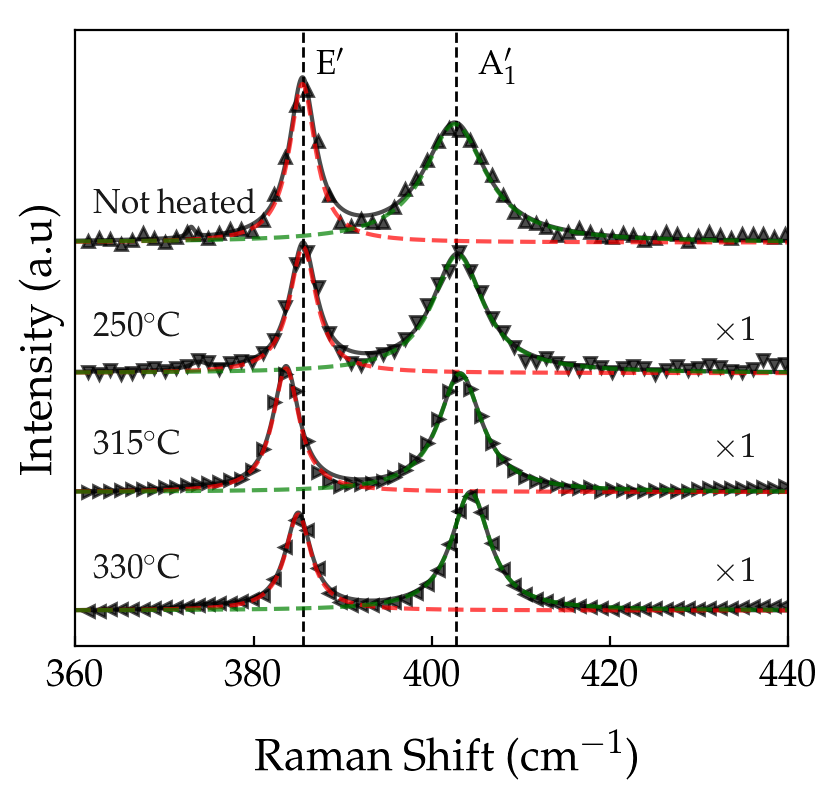
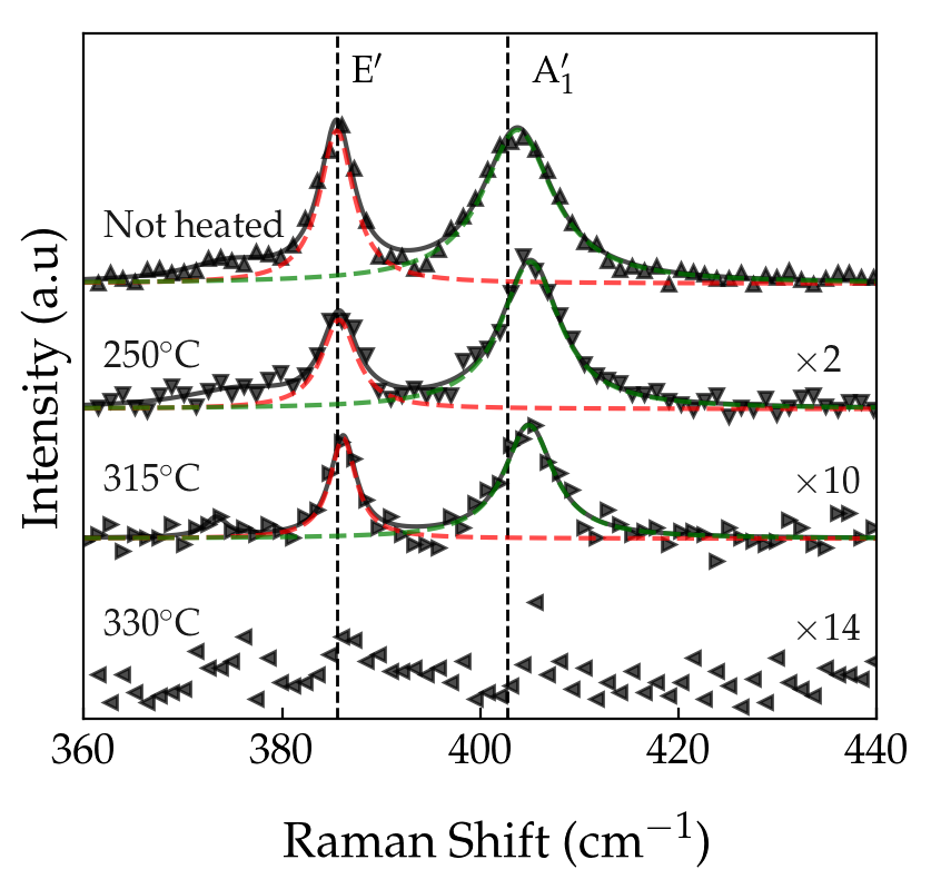
Ex-situ Raman spectroscopy was carried out using a WITec Alpha 300R system (532 nm laser) with a 100 objective (NA=0.95) (spot size 0.3 ) and a 1800 lines/mm grating. Raman maps were generated by taking four spectra per in both the x and y directions over large areas Delhaye and Dhamelincourt (1975). Each acquisition was for 0.05 s. The laser power was 1 mW or less to minimize damage to the samples. The spectra from a desired region were acquired by averaging. Lorentzian distributions were fitted to the Raman peaks as indicated in Figure 3.
Ex-situ scanning electron microscopy (SEM) was performed with a field emission SEM (Zeiss Supra fitted with a Gemini column, Zeiss Microscopy GmbH, Jena, Germany). The microscope was operated at a beam energy of 10 keV.
III Results
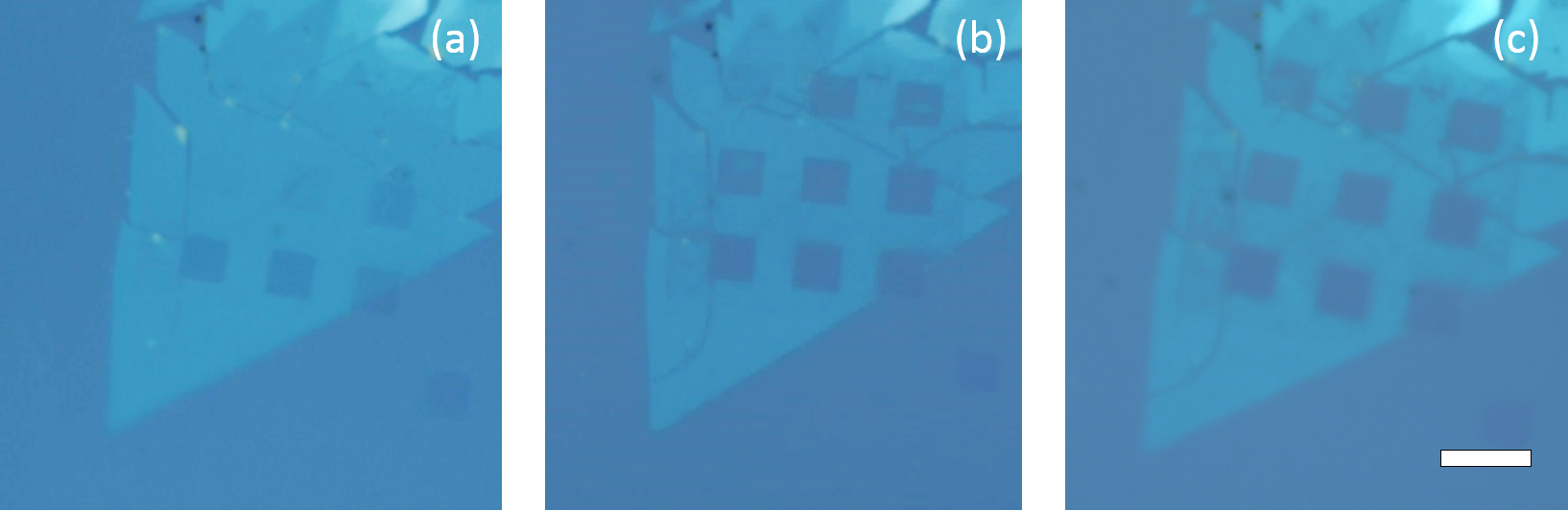
Figure 2(a) shows optical microscope images of an array of squares in a bilayer region of CVD MoS2 which were irradiated with 30 keV He+. The irradiation doses range from He+ cm-2 (which is not visible, in the top left) to He+ cm-2 (notably discolored, in the bottom right row). There is another square of irradiated substrate which is barely visible to the bottom right. Figure 2(b) shows the same region after heating for 50 mins at 330°C. All of the squares on MoS2 are now much more clearly visible and most (exluding the lowest doses) appear much more like the irradiated substrate, suggesting they have been etched. The minimum dose which resulted in etching of the MoS2 appears to be He+ cm-2 although some regions with doses up to He+ cm-2 were not fully etched. Doses above this were always sufficient to remove all material in a region after heat treatment. In addition, when the heating step was repeated for a further 50 minutes under the same conditions, even the lowest dose ( He+ cm region was almost completely etched, as shown in figure 2(c).
A new array of rectangles was irradiated in monolayer regions of CVD MoS2 for investigation with Raman spectroscopy. The irradiated patterns are overlaid on a low dose HIM image which is presented in Figure S1 along with Raman maps. Figure 3 shows two selected sets of MoS2 Raman spectra, both non-irradiated and irradiated (5 1014 He+ cm-2), before and after heating to different maximum temperatures. For the non-irradiated spectra in figure 3(a), a slight increase in peak separation and a narrowing of the peak are observed as the maximum temperature increases. For the irradiated spectra in figure 3(b), the results are more dramatic. As expected, the peak separation is increased even without heating, and it is further increased by heating in air. The Raman intensity is observed to decline sharply with heating and there are no clearly identifiable peaks after heating to 330°C. It should be noted that no residual oxides of molybdenum could be detected in the etched regions, suggesting the complete sublimation of MoOx (see Figure S2) Wachs and Roberts (2010); Diskus et al. (2012); Yang et al. (2012); Lafuente et al. (2015).
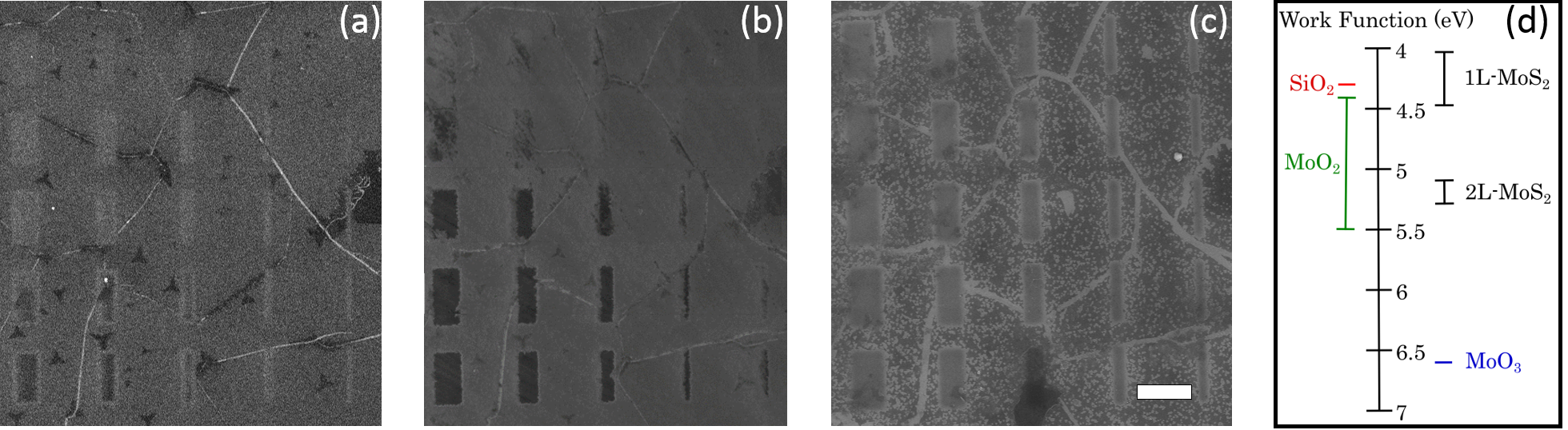
In order to further clarify the effects at different temperatures, another sample of monolayer CVD MoS2 was prepared and an array of rectangles of various widths and doses was irradiated in it. The sample was put through a series of heating steps lasting 10 mins at a maximum temperature which was iteratively increased from 300°C to 335°C in 5°C increments. Between each heating step the sample was imaged in a field emission SEM using a through-the-lens (TTL) or "inLens" detector, chosen for its particular sensitivity to the work function of the specimen. A selection of the SEM micrographs are shown in figure 4. They demonstrate the progression from irradiated MoS2 through to the complete etching of irradiated material after heating. Figure 4(a) shows low dose irradiated regions which are lighter than surrounding areas and higher dose regions which are slightly darker. After the 305°C step, figure 4(b) shows the same regions where those that received lower doses are still relatively unchanged and those that received higher doses are now very dark. Figure 4(c) shows the same regions once again after the 330°C step where all irradiated regions now appear to have been etched. Using an inLens detector, low work function materials typically appear bright and high work function materials appear dark. Changes in the signal intensity of a material in SEM images acquired in these conditions can be used to qualitatively infer changes in the material work function. The work function of monolayer MoS2 (4.0 eV) has been reported to increase as O2 becomes adsorbed to its surface Lee et al. (2016). The work functions of MoO2 and MoO3 are 4.4-5.5 eV and 6.6 eV respectively Bernhard (1999); Moosburger-Will et al. (2009); Guo and Robertson (2014).The range of work functions of possible materials in this system is represented in figure 4(d). The work function is expected to increase after exposure to oxygen, first because of adsorption (to 4.5 eV) Lee et al. (2016), and possibly again when the material is oxidized to MoOx if it remains in place (4.4-6.6 eV). The increased work function causes a darkening of the sample evident in figure 4(b), although the distinction between adsorption and oxidation is not initially clear here, as will be discussed further below. Should a region be observed to lighten after a heating step, it must be due to the oxidation reaction coupled with evaporation of the MoOx species, revealing the SiO2 substrate underneath which has a work function more similar to the starting material (4.3 eV) Yan et al. (2012).
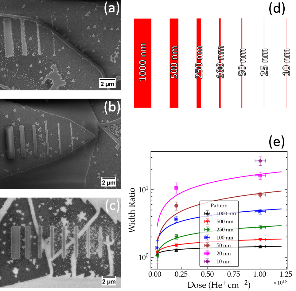
To investigate the effect of ion dose on the size of etched features, arrays of rectangles with descending widths were irradiated in monolayer MoS2 for different doses and etched at 330°C for 50 mins. These arrays are shown in figure 5(a),(b) and (c) for 2 He+ cm-2, 2 He+ cm-2 and 1 He+ cm-2 respectively. The rectangle widths are indicated schematically in figure 5(d), varying from left to right as follows: 1000, 500, 250, 100, 50, 20, 10, 5, 1 nm. Even the smallest width can be seen for the highest dose but only rectangles with irradiated widths of 250 nm or above are fully etched for the lowest dose. Narrower rectangles for the lowest dose are observed to be partially etched, being not contiguous. Other etching is observed to occur along previously hidden grain boundaries in figure 5(a) and (c). Figure 5(e) shows a graph of the width ratio (), defined as the SEM-measured width normalised to its designed width, against the delivered dose () for rectangles of different widths. Larger doses are required to ensure that the smallest patterned features are fully etched. Once above the threshold for etching, the effect of increasing the dose is to broaden the etched feature. The relationship between and is of the form:
| (2) |
where and are fitting parameters. From the 20 nm to the 1000 nm designed width rectangles, increases exponentially from to 136. At the same time, decreases exponentially from 0.45 to 0.064.
IV Discussion
The ion dose demonstrated to induce etching (cm-2) corresponds to an ion-induced defect density of about one in a thousand atoms. It is below the dose normally required to remove material by direct ion milling by 4 orders of magnitude. It was also less than the dose required for amorphisation or detectable change in stoichiometry by 2 to 4 orders of magnitude Fox et al. (2015).
Figure 6 shows several heat maps, representing a summary of salient data from the Raman and SEM experiments. We can use them to label several discrete stages separated by their temperature range. Stage 0 is the initial state of the irradiated MoS2, before the application of any heating step. When characterized, a dose-dependent increase in the frequency and width of the A peak along with an apparent increased work function are observed Mignuzzi et al. (2015); Maguire et al. (2018a); Klein et al. (2018); Maguire et al. (2018b). From the literature, these observations are consistent with the material being increasingly defective.
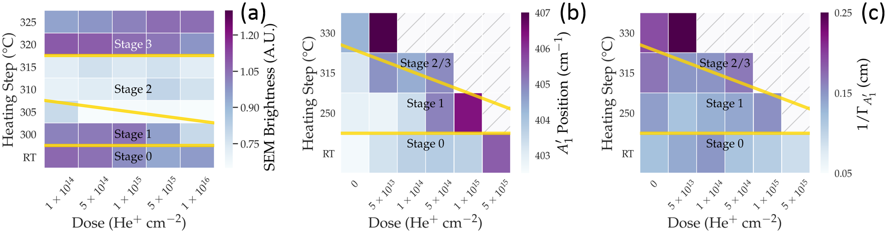
| # | Temp (°C) | Description | |||
|---|---|---|---|---|---|
| 0 | RT | All | H.D. | H.D. | Increased Defects |
| 1 | All | H.D. | H.D. | O2 Adsorption at Defect Sites | |
| 2 | All | All | All | O2 Adsorption to Saturation | |
| 3 | All – | All – | All | Oxidation |
Stage 1 is applicable after heating to temperatures 305°C. Unlike in stage 0, the position and width of the peak no longer increase together. While the frequency continues to increase, the peak is now observed to narrow and SEM brightness is slightly decreased. Oxygen adsorption has an electron withdrawing effect on adjacent MoS2. Therefore, these are clear indications of increased oxygen content and resulting p-type doping Chakraborty et al. (2012); Wu et al. (2013); Yamamoto et al. (2013a). In this range, oxidative etching is rarely noted in the literature and only for times much longer than those used in this work. The increased defect density caused by the ion irradiation has lowered the barrier for oxygen adsorption Fox et al. (2015); K. C. et al. (2015). Since these effects show such a strong dose relationship in stage 1, it seems that this stage is dominated by activity at the induced defect sites.
The regime between the temperatures of °C and °C is labelled as stage 2. Here, even the peak of non-irradiated and low dose MoS2 is now strongly affected. In addition, the apparent change in work function is now much more intense. This is attributed to a highly increased oxygen adsorption rate which is no longer dependent on defects as was the case in stage 1. The first etched pits in our non-irradiated material are observed at the top of this range suggesting that oxidation is beginning to occur significantly.
Stage III occurs at 320-325°C. By this stage, it is observed in the SEM images that brightness is now similar across all irradiated areas regardless of dose. This stage is therefore attributed to the complete oxidation and sublimation of Mo species leaving behind only the SiO2 substrate. The key characteristics of these stages are presented in table 2.
At the lower temperatures, the effect of ion dose is strong. However, at temperatures above 320°C, the distinction between irradiated and non-irradiated material begins to matter less and even non-irradiated MoS2 begins to etch. This can be seen in the SEM image in figure 4(c) and is also clear from Raman spectra results which show even the lowest doses having been fully etched after high temperature treatment. Here, curved lines of material near grain boundaries and many randomly positioned pits at native defect sites are observed to have been etched.
V Conclusion
In this work, ion irradiation has been successfully established as a high throughput tool for moderating the oxygen adsorption and oxidation of 2D MoS2. Previous studies have used oxidative etching for the doping and etching of MoS2 but this is the first report of doing so while asserting spatial control, leaving other non-irradiated regions relatively untouched. Region-specific, low dose and high throughput irradiation with He+ at 30 keV allowed thermal etching to be preferentially stimulated in discretionary regions. At heating temperatures comparable to the literature, doses as low as 1 He+ cm-2 showed a profound effect on oxidative etching. This method also avoids the use of resists which are a leading source of contamination in 2D material based devices. A breakdown of effects at different temperatures using Raman spectroscopy and SEM was also provided, developing understanding of the stability of defective MoS2 in potentially oxidative environments.
Additional information
Supplementary Information accompanies this paper at **. It includes Raman maps and Raman spectra in relation to the absence of oxides.
Acknowledgements
The authors thank the staff at the Advanced Microscopy Laboratory (AML), CRANN, Trinity College Dublin. We acknowledge support from the following grants: Science Foundation Ireland [grant numbers: 12/RC/2278, 15/SIRG/3329, 11/PI/1105, 07/SK/I1220a, 15/IA/3131 and 08/CE/I1432] and Irish Research Council [grant number: GOIPG/2014/972]. Figure 1 was prepared with use of the Vesta software package Momma and Izumi (2011).
Bibliography
References
- Wu et al. (2013) J. Wu, H. Li, Z. Yin, H. Li, J. Liu, X. Cao, Q. Zhang, and H. Zhang, Small 9, 3314 (2013).
- Zhou et al. (2013) H. Zhou, F. Yu, Y. Liu, X. Zou, C. Cong, C. Qiu, T. Yu, Z. Yan, X. Shen, L. Sun, B. I. Yakobson, and J. M. Tour, Nano Research 6, 703 (2013).
- Yamamoto et al. (2013a) M. Yamamoto, T. L. Einstein, M. S. Fuhrer, and W. G. Cullen, The Journal of Physical Chemistry C 117, 25643 (2013a).
- Neupane et al. (2016) G. P. Neupane, K. P. Dhakal, H. Kim, J. Lee, M. S. Kim, G. Han, Y. H. Lee, and J. Kim, Journal of Applied Physics 120, 1 (2016).
- Rao et al. (2017) R. Rao, A. E. Islam, P. M. Campbell, E. M. Vogel, and B. Maruyama, 2D Materials 4 (2017).
- Kam and Parkinson (1982) K. K. Kam and B. A. Parkinson, The Journal of Physical Chemistry 86, 463 (1982).
- Mak et al. (2010) K. F. Mak, C. Lee, J. Hone, J. Shan, and T. F. Heinz, Physical Review Letters 105, 136805 (2010).
- Lee et al. (2010) C. Lee, H. Yan, L. E. Brus, T. F. Heinz, J. Hone, and S. Ryu, ACS Nano 4, 2695 (2010).
- Splendiani et al. (2010) A. Splendiani, L. Sun, Y. Zhang, T. Li, J. Kim, C. Y. Chim, G. Galli, and F. Wang, Nano Letters 10, 1271 (2010).
- Liu et al. (2013) Y. Liu, H. Nan, X. Wu, W. Pan, W. Wang, J. Bai, W. Zhao, and L. Sun, ACS Nano 7, 4202 (2013).
- Pu et al. (2012) J. Pu, Y. Yomogida, K. K. Liu, L. J. Li, Y. Iwasa, and T. Takenobu, Nano Letters 12, 4013 (2012).
- Lopez-Sanchez et al. (2013) O. Lopez-Sanchez, D. Lembke, M. Kayci, A. Radenovic, and A. Kis, Nature Nanotechnology 8, 497 (2013).
- Zhang et al. (2014) J. Zhang, S. Najmaei, H. Lin, and J. Lou, Nanoscale 6, 5279 (2014).
- Zhan et al. (2012) Y. Zhan, Z. Liu, S. Najmaei, P. M. Ajayan, and J. Lou, Small 8, 966 (2012).
- Lee et al. (2012) Y. H. Lee, X. Q. Zhang, W. Zhang, M. T. Chang, C. T. Lin, K. D. Chang, Y. C. Yu, J. T. W. Wang, C. S. Chang, L. J. Li, and T. W. Lin, Advanced materials 24, 2320 (2012).
- Song et al. (2015) I. Song, C. Park, and H. C. Choi, RSC Adv. 5, 7495 (2015).
- Qiu et al. (2013) H. Qiu, T. Xu, Z. Wang, W. Ren, H. Nan, Z. Ni, Q. Chen, S. Yuan, F. Miao, F. Song, G. Long, Y. Shi, L. Sun, J. Wang, and X. Wang, Nature Communications 4, 2642 (2013).
- Fivaz and Mooser (1967) R. Fivaz and E. Mooser, Physical Review 163, 743 (1967).
- Ballou and Ross (1953) E. V. Ballou and S. Ross, The Journal of Physical Chemistry 57, 653 (1953).
- Ross and Sussman (1955) S. Ross and A. Sussman, The Journal of Physical Chemistry 59, 889 (1955).
- Lansdown (1999) A. R. Lansdown, Molybdenum Disulphide Lubrication (Elsevier B.V., 1999) pp. 41–44.
- Khare and Burris (2013) H. S. Khare and D. L. Burris, Tribology Letters 52, 485 (2013).
- Gan et al. (2016) L. Gan, Y. Cheng, U. Schwingenschlögl, Y. Yao, Y. Zhao, X. X. Zhang, and W. Huang, Applied Physics Letters 109 (2016).
- Yamamoto et al. (2013b) M. Yamamoto, W. Cullen, T. Einstein, and M. S. Fuhrer, in APS March Meeting Abstracts, Vol. 1 (2013) p. 6004.
- Azcatl et al. (2014) A. Azcatl, S. McDonnell, K. C. Santosh, X. Peng, H. Dong, X. Qin, R. Addou, G. I. Mordi, N. Lu, J. Kim, M. J. Kim, K. Cho, and R. M. Wallace, Applied Physics Letters 104 (2014).
- Huang et al. (2013) Y. Huang, J. Wu, X. Xu, Y. Ho, G. Ni, and Q. Zou, Nano Research 6, 200 (2013).
- Zhu et al. (2016) H. Zhu, X. Qin, L. Cheng, A. Azcatl, J. Kim, and R. M. Wallace, ACS Applied Materials and Interfaces 8, 19119 (2016).
- Jadwiszczak et al. (2017) J. Jadwiszczak, C. O’Callaghan, Y. Zhou, D. S. Fox, E. Weitz, D. Keane, I. O’Reilly, C. Downing, A. Shmeliov, P. Maguire, J. J. Gough, C. McGuinness, M. S. Ferreira, A. L. Bradley, J. J. Boland, V. Nicolosi, and H. Zhang, Science Advances 4, eaao5031 (2017).
- Jadwiszczak et al. (2019) J. Jadwiszczak, G. Li, C. P. Cullen, J. J. Wang, P. Maguire, G. S. Duesberg, J. G. Lunney, and H. Zhang, Applied Physics Letters 114 (2019).
- Schweiger et al. (2002) H. Schweiger, P. Raybaud, G. Kresse, and H. Toulhoat, Journal of Catalysis 207, 76 (2002).
- Jaramillo et al. (2007) T. F. Jaramillo, K. P. Jørgensen, J. Bonde, J. H. Nielsen, S. Horch, and I. Chorkendorff, Science 317, 100 (2007).
- K. C. et al. (2015) S. K. C., R. C. Longo, R. M. Wallace, and K. Cho, Journal of Applied Physics 117 (2015).
- Lince and Frantz (2000) J. Lince and P. Frantz, Tribology Letters 9 (2000).
- Hu et al. (2015) J. Hu, S. Wu, Y. Ma, X. Yang, Z. Li, H. Liu, Q. Huo, J. Guan, and Q. Kan, New J. Chem. 39, 5459 (2015).
- Wieting and Verble (1971) T. J. Wieting and J. L. Verble, Physical Review B 3, 4286 (1971).
- Chen and Wang (1974) J. M. Chen and C. S. Wang, Solid State Communications 14, 857 (1974).
- Windom et al. (2011) B. C. Windom, W. G. Sawyer, and D. W. Hahn, Tribology Letters 42, 301 (2011).
- Livneh and Spanier (2015) T. Livneh and J. E. Spanier, 2D Materials 2, 035003 (2015).
- Stacy and Hodul (1985) A. M. Stacy and D. T. Hodul, Journal of Physics and Chemistry of Solids 46, 405 (1985).
- Frey et al. (1999) G. L. Frey, R. Tenne, M. J. Matthews, M. S. Dresselhaus, and G. Dresselhaus, Physical Review B 60, 2883 (1999).
- Rice et al. (2013) C. Rice, R. J. Young, R. Zan, U. Bangert, D. Wolverson, T. Georgiou, R. Jalil, and K. S. Novoselov, Physical Review B 87, 081307 (2013).
- Chakraborty et al. (2012) B. Chakraborty, A. Bera, D. V. S. Muthu, S. Bhowmick, U. V. Waghmare, and A. K. Sood, Physical Review B 85 (2012).
- Li et al. (2012a) H. Li, Q. Zhang, C. C. R. Yap, B. K. Tay, T. H. T. Edwin, A. Olivier, and D. Baillargeat, Advanced Functional Materials 22, 1385 (2012a).
- Li et al. (2012b) H. Li, Z. Yin, Q. He, H. Li, X. Huang, G. Lu, D. W. H. Fam, A. I. Y. Tok, Q. Zhang, and H. Zhang, Small 8, 63 (2012b).
- Zhao et al. (2013) Y. Zhao, X. Luo, H. Li, J. Zhang, P. T. Araujo, C. K. Gan, J. Wu, H. Zhang, S. Y. Quek, M. S. Dresselhaus, and Q. Xiong, Nano Letters 13, 1007 (2013).
- McCreary et al. (2016) A. McCreary, R. Ghosh, M. Amani, J. Wang, K. A. N. Duerloo, A. Sharma, K. Jarvis, E. J. Reed, A. M. Dongare, S. K. Banerjee, M. Terrones, R. R. Namburu, and M. Dubey, ACS Nano 10, 3186 (2016).
- Shi et al. (2013) Y. Shi, J. K. Huang, L. Jin, Y. T. Hsu, S. F. Yu, L. J. Li, and H. Y. Yang, Scientific Reports 3, 1839 (2013).
- Fox et al. (2015) D. S. Fox, Y. Zhou, P. Maguire, A. O’Neill, C. O’Coileáin, R. Gatensby, A. M. Glushenkov, T. Tao, G. S. Duesberg, I. V. Shvets, M. Abid, M. Abid, H. C. Wu, Y. Chen, J. N. Coleman, J. F. Donegan, and H. Zhang, Nano Letters 15, 5307 (2015).
- Klein et al. (2018) J. Klein, A. Kuc, A. Nolinder, M. Altzschner, J. Wierzbowski, F. Sigger, F. Kreupl, J. J. Finley, U. Wurstbauer, A. W. Holleitner, and M. Kaniber, 2D Materials 5, 011007 (2018).
- Maguire et al. (2018a) P. Maguire, D. S. Fox, Y. Zhou, Q. Wang, M. O’Brien, J. Jadwiszczak, C. P. Cullen, J. B. McManus, S. Bateman, N. McEvoy, G. S. Duesberg, and H. Zhang, Physical Review B 98, 134109 (2018a).
- Maguire et al. (2018b) P. Maguire, C. Downing, J. Jadwiszczak, M. O’Brien, D. Keane, J. B. McManus, G. S. Duesberg, V. Nicolosi, N. McEvoy, and H. Zhang, arXiv , 1 (2018b), arXiv:arXiv:1812.05543v2 .
- Iberi et al. (2016) V. Iberi, L. Liangbo, A. V. Ievlev, M. G. Stanford, M. W. Lin, X. Li, M. Mahjouri-Samani, S. Jesse, B. G. Sumpter, S. V. Kalinin, D. C. Joy, K. Xiao, A. Belianinov, and O. S. Ovchinnikova, Scientific Reports 6 (2016).
- Stanford et al. (2016) M. G. Stanford, P. R. Pudasaini, A. Belianinov, N. Cross, J. H. Noh, M. R. Koehler, D. G. Mandrus, G. Duscher, A. J. Rondinone, I. N. Ivanov, T. Z. Ward, and P. D. Rack, Scientific Reports , 27276 (2016).
- Nanda et al. (2017) G. Nanda, G. Hlawacek, S. Goswami, K. Watanabe, T. Taniguchi, and P. F. A. Alkemade, Carbon 119, 419 (2017).
- Zhou et al. (2016) Y. Zhou, P. Maguire, J. Jadwiszczak, M. Muruganathan, H. Mizuta, and H. Zhang, Nanotechnology 27, 325302 (2016).
- O’Brien et al. (2014) M. O’Brien, N. McEvoy, T. Hallam, H. Y. Kim, N. C. Berner, D. Hanlon, K. Lee, J. N. Coleman, and G. S. Duesberg, Scientific Reports 4, 7374 (2014).
- Delhaye and Dhamelincourt (1975) M. Delhaye and P. Dhamelincourt, Journal of Raman Spectroscopy 3, 33 (1975).
- Wachs and Roberts (2010) I. E. Wachs and C. A. Roberts, Chemical Society Reviews 39, 5002 (2010).
- Diskus et al. (2012) M. Diskus, O. Nilsen, H. Fjellvag, S. Diplas, P. Beato, C. Harvey, E. van Schrojenstein Lantman, and B. M. Weckhuysen, Journal of Vacuum Science & Technology A Vacuum Surfaces and Films 30 (2012).
- Yang et al. (2012) L. Yang, L. Liu, Y. Zhu, X. Wang, and Y. Wu, Journal of Materials Chemistry 22, 13148 (2012).
- Lafuente et al. (2015) B. Lafuente, R. T. Downs, H. Yang, and N. Stone, Highlights in Mineralogical Crystallography, edited by T. Armbruster and M. D. Danisi (De Gruyter, 2015) pp. 1–29.
- Lee et al. (2016) S. Y. Lee, U. J. Kim, J. Chung, H. Nam, H. Y. Jeong, G. H. Han, H. H. Kim, H. M. Oh, H. Lee, H. H. Kim, Y. G. Roh, J. Kim, S. W. Hwang, Y. Park, and Y. H. Lee, ACS Nano 10, 6100 (2016).
- Bernhard (1999) J. M. Bernhard, Work Function Study of Iridium Oxide and Molybdenum Using UPS and Simultaneous Fowler-Norheim I-V Plots with Field Emission Energy Distributions, Ph.D. thesis, University of North Texas (1999).
- Moosburger-Will et al. (2009) J. Moosburger-Will, J. Kündel, M. Klemm, S. Horn, P. Hofmann, U. Schwingenschlögl, and V. Eyert, Physical Review B 79, 115113 (2009).
- Guo and Robertson (2014) Y. Guo and J. Robertson, Applied Physics Letters 105, 222110 (2014).
- Yan et al. (2012) R. Yan, Q. Zhang, W. Li, I. Calizo, T. Shen, C. A. Richter, A. R. Hight-Walker, X. Liang, A. Seabaugh, D. Jena, H. G. Xing, D. J. Gundlach, and N. V. Nguyen, Applied Physics Letters 101, 022105 (2012).
- Mignuzzi et al. (2015) S. Mignuzzi, A. J. Pollard, N. Bonini, B. Brennan, I. S. Gilmore, M. A. Pimenta, D. Richards, and D. Roy, Physical Review B 91, 195411 (2015).
- Momma and Izumi (2011) K. Momma and F. Izumi, Journal of Applied Crystallography 44, 1272 (2011).