Intrinsic persistent spin helix in two-dimensional group-IV monochalcogenide (: Sn, Ge; : S, Se, Te) monolayer
Abstract
Energy-saving spintronics are believed to be implementable on the systems hosting persistent spin helix (PSH) since they support an extraordinarily long spin lifetime of carriers. However, achieving the PSH requires a unidirectional spin configuration in the momentum space, which is practically non-trivial due to the stringent conditions for fine-tuning the Rashba and Dresselhaus spin-orbit couplings. Here, we predict that the PSH can be intrinsically achieved on a two-dimensional (2D) group-IV monochalcogenide monolayer, a new class of the noncentrosymmetric 2D materials having in-plane ferroelctricity. Due to the point group symmetry in the monolayer, a unidirectional spin configuration is preserved in the out-of-plane direction and thus maintains the PSH that is similar to the [110] Dresselhaus model in the [110]-oriented quantum well. Our first-principle calculations on various (: Sn, Ge; : S, Se, Te) monolayers confirmed that such typical spin configuration is observed, in particular, at near the valence band maximum where a sizable spin splitting and a substantially small wavelength of the spin polarization are achieved. Importantly, we observe reversible out-of-plane spin orientation under opposite in-plane ferroelectric polarization, indicating that an electrically controllable PSH for spintronic applications is plausible.
pacs:
Valid PACS appear hereI INTRODUCTION
Recent development of spintronics relies on the new pathway for exploiting electron’s spin in semiconductors by utilizing the effect of spin-orbit coupling (SOC)Nitta et al. (1997); Manchon et al. (2015). In a system with lack of inversion symmetry, the SOC induces an effective magnetic field or known as a spin-orbit field (SOF) acting on spin, so that the effective SOC Hamiltonian can be expressed as
| (1) |
where is the SOF vector, is the wave vector representing momentum of electrons, is the Pauli matrices vector, and is the strength of the SOC that is proportional to magnitude of local electric field induced by the crystal inversion asymmetry. Since the SOF is odd in the electron’s wave vector , as was firstly demonstrated by Dresselhauss Dresselhaus (1955) and Rashba Rashba (1960), the SOC lifts Kramers’ spin degeneracy and leads to a complex -dependent spin configuration of the electronic bands. In particular interest is driven due to a possibility to manipulate this spin configuration by using an external electric field to create non-equilibrium spin polarization Kuhlen et al. (2012), leading to various important phenomena such as spin Hall effect Qi et al. (2006), spin galvanic effect Ganichev et al. (2002), and spin ballistic transport Lu et al. (1998), thus offering for realization of spintronics device such as spin-field effect transistor (SFET)Datta and Das (1990).
From practical perspective, materials having strong Rashba SOC have generated significant interest since they allow for electrostatic manipulation of the spin states Nitta et al. (1997); Chuang et al. (2009), paving the way towards non-charge-based computing and information processing Manchon et al. (2015). However, the strong SOC is also known to induce the undesired effect of causing spin decoherence Dyakonov and Perel (1972), which plays an adverse role in the spin lifetime. In a diffusive transport regime, impurities and defects act as scatters which change the momentum of electron and simultaneously randomize the spin due to momentum-dependent SOF, leading to the fast spin decoherence through the Dyakonov-Perel (DP) mechanism of spin-relaxationDyakonov and Perel (1972).This process induces spin dephasing and a loss of the spin signal, such that the spin lifetime significantly reduces, thus limiting the performance of potential spintronic devices.
A possible way to overcome this obstacle is to eliminate the problem of the spin dephasing by suppressing the DP spin relaxation. This can be achieved, in particular, by designing a structure where the SOF orientation is enforced to be unidirectional, preserving a unidirectional spin configuration in the momentum space. In such situation, electron motion together with the spin precession around the unidirectional SOF leads to a spatially periodic mode of the spin polarization known as persistent spin helix (PSH)Bernevig et al. (2006); Schliemann (2017). The corresponding spin wave mode protects the spins of electron from the dephasing due to spin rotation symmetry, which is robust against spin-independent scattering and renders an extremely long spin lifetime Bernevig et al. (2006); Altmann et al. (2014). Previously, the PSH has been demonstrated on various [001]-oriented semiconductors quantum well (QW) Koralek et al. (2009); Walser et al. (2012); Schönhuber et al. (2014); Ishihara et al. (2014); Kohda et al. (2012); Sasaki et al. (2014) having equal strength of the Rashba and Dresselhauss SOC, or on [110]-oriented semiconductor QW Chen et al. (2014) in which the SOC is described by the [110] Dreseelhauss model. Here, for the former, the spin configurations are enforced to be unidirectional in the in-plane [110] direction, whereas for the latter, they are oriented in the out-of-plane [001] direction. Similar to the [110]-oriented QW, the PSH state has recently been reported for LaAlO3/SrTiO3 interface Yamaguchi and Ishii (2017), ZnO [10-10] surface Absor et al. (2015), halogen-doped SnSe monolayer Absor and Ishii (2019), and WO2Cl2 monolayerAi et al. (2019). Although the PSH has been widely studied on various QW systems Koralek et al. (2009); Walser et al. (2012); Schönhuber et al. (2014); Ishihara et al. (2014); Kohda et al. (2012); Sasaki et al. (2014), it is practically non-trivial due to the stringent conditions for fine-tuning the Rashba and Dresselhaus SOCs. Therefore, it would be desirable to find a new class of material which intrinsically supports the PSH.
In this paper, we show that the PSH can be intrinsically achieved on a two-dimensional (2D) group-IV monochalcogenide monolayer, a new class of noncentrosymmetric 2D materials having in-plane ferroelctricityFei et al. (2016); Barraza-Lopez et al. (2018); Kaloni et al. (2019); Wan et al. (2017); Hanakata et al. (2016). On the basis of density-functional theory (DFT) calculations on various (: Sn, Ge; : S, Se, Te) monolayers, supplemented with symmetry analysis, we find that a unidirectional spin orientation is preserved in the out-of-plane direction, yielding a PSH that is similar to the [110] Dresselhaus model in the [110]-oriented QW. Such typical spin configuration is observed, in particular, at near the valence band maximum, having a sizable spin splitting and small wavelength of the spin polarization. More interestingly, we observe reversible out-of-plane spin orientation under opposite in-plane ferroelectric polarization, suggesting that an electrically controllable PSH is achievable, which is useful for spintronic applications.
II Computational details
We performed first-principles calculations by using DFT within the generalized gradient approximation (GGA) Perdew et al. (1996) implemented in the OpenMX code Ozaki et al. (2009). Here, we adopted norm-conserving pseudopotentials Troullier and Martins (1991) with an energy cutoff of 350 Ry for charge density. The k-point mesh was used. The wave functions were expanded by linear combination of multiple pseudoatomic orbitals generated using a confinement scheme Ozaki (2003); Ozaki and Kino (2004), where two -, two -, two -character numerical pseudo-atomic orbitals were used. The SOC was included in the DFT calculations by using -dependent pseudopotentials (Theurich and Hill, 2001). The spin textures in the momentum space were calculated using the spin density matrix of the spinor wave functions obtained from the DFT calculations as we applied recently on various 2D materials (Absor et al., 2015; Absor and Ishii, 2019; Absor et al., 2018a, 2016, 2017, b).
| monolayer | (Å) | (Å) | (Å) | (Å) | (eV) |
|---|---|---|---|---|---|
| SnS | 4.01 | 4.39 | 2.71 | 2.63 | 1.38 |
| SnSe | 4.34 | 4.49 | 2.89 | 2.7 | 0.98* |
| SnTe | 4.54 | 4.58 | 3.31 | 3.04 | 0.85 |
| GeS | 3.68 | 4.40 | 2.53 | 2.46 | 1.45 |
| GeSe | 3.99 | 4.26 | 2.72 | 2.57 | 1.10* |
| GeTe | 4.27 | 4.47 | 2.95 | 2.81 | 0.92 |
In our DFT calculations, we considered ferroelectric phase of the monolayer having black phosporene-type structure Gomes and Carvalho (2015); Appelbaum and Li (2016). The minimum energy pathways of ferroelectric transitions were calculated using nudged elestic band (NEB) methodHenkelman and Jónsson (2000) based on the interatomic forces and total energy obtained from DFT caclulations. The Ferroelectric polarization was calculated using Berry phase approach King-Smith and Vanderbilt (1993), where both electronic and ionic contributions were considered. We used a periodic slab to model the monolayer, where a sufficiently large vacuum layer (20 Å) is applied in order to avoid interaction between adjacent layers. We used the axes system where layers are chosen to sit on the plane, while the axis is taken to be parallel to the puckering direction [Fig. 1(a)]. The geometries were fully relaxed until the force acting on each atom was less than 1 meV/Å. The optimized structural-related parameters are summarized in Table 1, where overall are in good agreement with previously reported data Xu et al. (2017); Gomes and Carvalho (2015); Wan et al. (2017).
III Results and Discussion
III.1 Symmetry-protected PSH state in monolayer
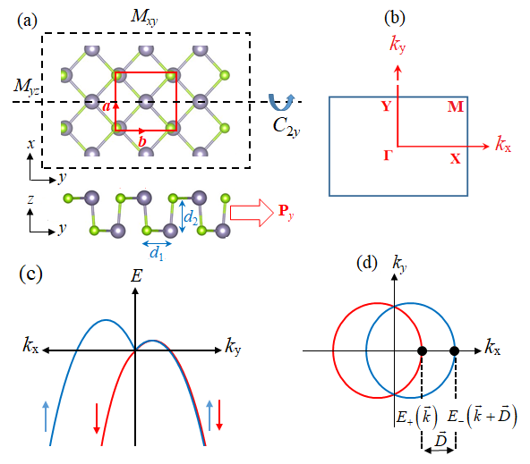
To predict the PSH state in the monolayer, we firstly derive an effective low energy Hamiltonian by using symmetry analysis. As shown in Fig. 1(a), the crystal structures of the ML has black phosporene-type structures where the symmetry group is isomorphic to or space group Appelbaum and Li (2016); Gomes and Carvalho (2015). There are four symmetry operations in the crystal lattice of the monolayer [Fig. 1(a)]: (i) identity operation ; (ii) twofold screw rotation (twofold rotation around the axis, , followed by translation of ), where and is the lattice parameters along and directions, respectively; (iii) glide reflection (reflection with respect to the plane followed by translation ); and (iv) reflection with respect to the plane. The effective Hamiltonian can be constructed by taking into account all symmetry operations in the little group of the wave vector in the reciprocal space.
| Symmetry operation | ||
|---|---|---|
Let be a high symmetry point in the first Brillouin zone (FBZ) where a pair of spin-degenerate eigen states exsist in the valence band maximum (VBM) or conduction band minimum (CBM). This degeneracy appers due to time reversal symmetry for which the condition that is satisfied, where is the 2D reciprocal-lattice vector. Such points are located at the center of the FBZ ( point), or some points that are located at the boundary of the FBZ such as , , and points for a primitive rectangular lattice [Fig. 1(b)]. The band dispersion around the point can be deduced by identifying all symmetry-allowed terms so that is obtained, where denotes all symmetry operations belonging to the little group of the point, supplemented by time-reversal symmetry .
For simplicity, let we assume that the little group of the wave vector at the point belongs to the point group similar to that of the crystal in the real space. Therefore, the wave vector and spin vector can be transformed according to the symmetry operation in the point group and time reversal symmetry . The corresponding transformation for the and are listed in Table II. Collecting all terms which are invariant with respect to the symmetry operation, we obtain the following effective Hamiltonian up to third order correction of Schliemann (2017):
| (2) |
where is the nearly free electron/hole energy, defined as is originated from the contribution of the -linear parameter and the correction provided by the third order parameters ( and ), corresponds to the third order parameters by the relation , and is the angle of the momentum with respect to the -axis defined as . Solving the eigenvalue problem involving the Hamiltonian of Eq. (2) yields split-split energy dispersions:
| (3) |
These dispersions are schematically illustrated in Fig. 1(c) showing a highly anisotropic spin splitting.
Since the Hamiltonian of Eq. (2) is only coupled with , neglecting all the cubic terms leads to the symmetry of the Hamiltonian Schliemann (2017); Bernevig et al. (2006),
| (4) |
with the energy dispersions,
| (5) |
Importantly, these dispersions have the shifting property: , where is the shifting wave vector. As a result, constant-energy cut shows two Fermi loops whose centers are displaced from their original point by as schematically shown in Fig. 1(d).
Since the component of the spin operator commutes with this Hamiltonian of Eq. (4), , the spin operator is a conserved quantity. Here, expectation value of the spin only has the out-of-plane component: at any wave vector except for , resulting in the unidirectional out-of-plane spin configuration in the momentum space [Fig. 1(d)]. In such situation, the unidirectional out-of-plane SOF is achieved, implying that the electron motion accompanied by the spin precession around the SOF form a spatially periodic mode of the spin polarization, yielding the PSH that is similar to the [110] Dresselhaus model Bernevig et al. (2006) as recently demonstrated on the [110]-oriented semiconductor QW(Chen et al., 2014).
In the next section, we discuss our results from the first-principles DFT calculations on various (: Sn, Ge; : S, Se, Te) monolayers to confirm the above predicted PSH.
III.2 DFT analysis of monolayer
Figure 2 shows the electronic band structures of various (: Sn, Ge; : S, Se, Te) monolayers calculated along the selected paths in the FBZ corresponding to the density of states (DOS) projected to the atomic orbitals. Without including the SOC, it is evident that there are two equivalent extrema valleys characterizing the VBM and CBM located at the points that are not time reversal invariant. Consistent with previous calculationsWan et al. (2017); Gomes and Carvalho (2015); Xu et al. (2017), the monolayers show indirect band gap (except for Se monolayer), where the VBM and CBM are located along the - and - lines, respectively. Overall, the calculated band gap [see Table I] is in a good agreement with previous results under GGA-PBE level Gomes and Carvalho (2015); Xu et al. (2017). Our calculated results of the DOS projected to the atomic orbitals confirmed that the - and - orbitals contributes dominantly to the VBM, while the CBM is mainly originated from the contribution of the - and - orbitals.
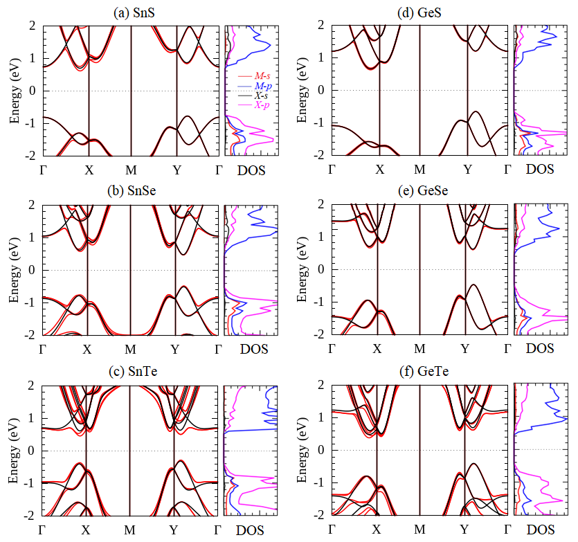
Turning the SOC strongly modifies the electronic band structures of the monolayers [Fig. 2]. Importantly, a sizable splitting of the bands produced by the SOC is observed at some high symmetry points and along certain paths in the FBZ. This splitting is especially pronounced around the X and Y points near both the VBM and CBM. However, there are special high-symmetry lines and points in the FBZ where the splitting is zero. This is in particular, the case for - line, where the wave vector is parallel to the ferroelectric polarization along the direction.
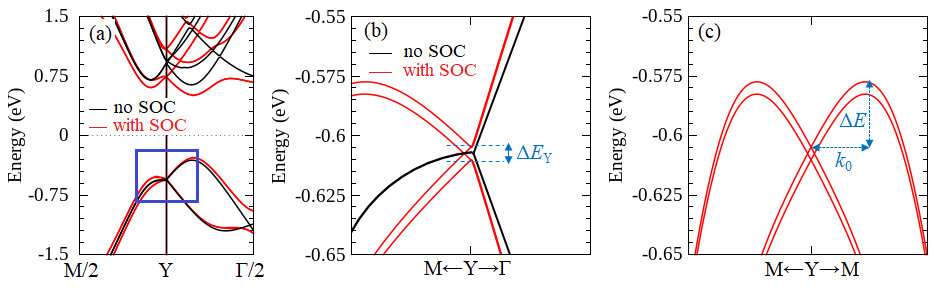
To analyze the properties of the spin splitting, we consider SnTe monolayer as a representative example of the monolayer. Here, we focus our attention on the bands near the VBM (including spin) around the Y point due to the large spin splitting as highligted by the blue lines in Fig. 3(a). Without the SOC, it is clearly seen from the band dispersion that fourfold degenerate state is visible at the point [Fig. 3(b)]. Taking into account the SOC, this degeneracy splits into two pair doublets with the splitting energy of meV [Fig. 3(c)]. Although these doublets remain at the along the - line, they split into a singlet when moving away along the - line, yielding a highly anisotropic spin splitting.
To clarify the origin of the anisotropic splitting around the point near the VBM, we discuss our system based on the symmetry argument. At the point, the little group of the wave vector belongs to the point groupAppelbaum and Li (2016). As previously mentioned that the point group contains the rotation symmetry around the -axis. Applying the rotation twice to the Bloch wave function, we have , thus we obtain that . We further define an antiunitary symmetry operator, , so that for spin half system. Therefore, at the point (), we find that , thus the Bloch states are double degenerate.
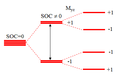
In addition, there is also mirror symmetry in the point group, which commutes with Hamiltonian of the crystal, . By operating symmetry to the Bloch states, we find that . Accordingly, the Bloch states can be labelled using the eigenvalues, i.e., . Here, for the point (), we find that , thus we obtain and . Therefore, there are two conjugated doublets at the point, or , which is distinguished by the eigenvalues as schematically shown in Fig. 4. These conjugated doublets are preserved along the - line but they split into singlet when moving to the - line, which are protected by the and symmtery operations. As a result, the strong anisotropic splitting is achieved, which is in fact consistent well with our DFT results shown in Fig. 3(c).
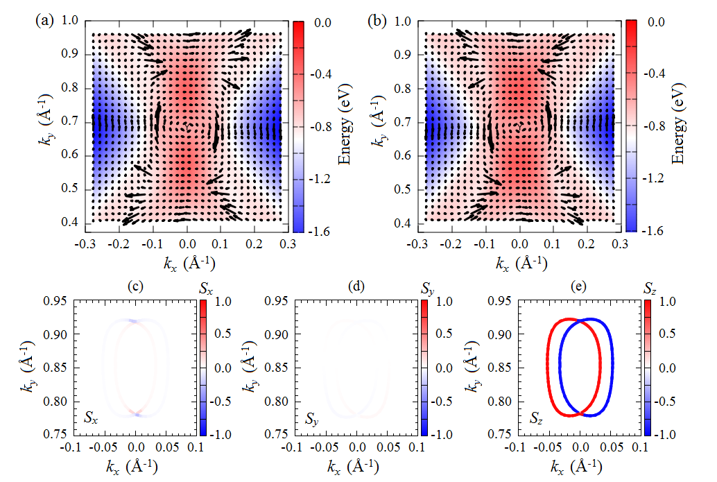
To further demonstrate the nature of the observed anisotropic splitting around the point near the VBM, we show in Figs. 5(a) and 5(b) the energy profiles of the spin textures for the upper and lower bands, respectively. It is found that a complex pattern of the spin polarization is observed around the point, which is remarkably different either from Rashba- and Dresselhaus-like spin textures. This is in contrast to the widely studied 2D materials such as PtSe2 Absor et al. (2018a); Yao et al. (2017), BiSb Liu et al. (2013), LaOBiS2 Singh and Romero (2017), and polar transition metal dichalcogenide Absor et al. (2017, 2018b), where the Rashba-like spin textures are identified. In particular, we observe a unifrom spin polarization close to the VBM, which persists in a region located at about 0.1 Å-1 from point along the - and - lines [see the region with red colour in Fig. 5(a)-(b)]. By carefully analyzing the spin textures measured at the constant energy cut of 1 meV below the VBM, we confirmed that this peculiar spin polarization is mostly dominated by the out-of-plane component [Fig. 5(e)] rather than the in-plane ones (, ) [Fig. 5(c)-(d)], leading to the unidirectional out-of-plane spin textures. On the other hand, the constant-energy cut also induces the Fermi lines characterized by the shifted two circular loops along the - () direction and the degenerated nodal point along the - () direction. Both the spin textures and Fermi lines are agree well with our Hamiltonian model derived from the symmetry analysis. Since the spin textures are uniformly oriented in the out-of-plane direction, the unidirectional out-of-plane SOF is achieved, maintaining the PSH that is similar to the [110] Dresselhauss model(Bernevig et al., 2006). Therefore, it is expected that the DP mechanism of the spin relaxation is suppressed, potentially ensurring to induce an extremely long spin lifetime.
| Systems | (eVÅ) | (nm) | Reference |
|---|---|---|---|
| monolayer | |||
| SnS | 0.09 | 1.5 | This work |
| SnSe | 0.74 | 44.85 | This work |
| SnTe | 1.20 | 7.13 | This work |
| GeS | 0.071 | 8.9 | This work |
| GeSe | 0.57 | 91.84 | This work |
| GeTe | 1.67 | 1.82 | This work |
| Interface | |||
| GaAs/AlGaAs | (3.5-4.9) | (7.3-10) | Ref.Walser et al. (2012) |
| 2.77 | 5.5 | Ref.Schönhuber et al. (2014) | |
| InAlAs/InGaAs | 1.0 | Ref.Ishihara et al. (2014) | |
| 2.0 | Ref.Sasaki et al. (2014) | ||
| LaAlO3/SrTiO3 | 7.49 | 0.098 | Ref.Yamaguchi and Ishii (2017) |
| Surface | |||
| ZnO(10-10) surface | 34.78 | 1.9 | Ref.Absor et al. (2015) |
| Bulk | |||
| BiInO3 | 1.91 | 2.0 | Ref.Tao and Tsymbal (2018) |
| 2D monolayer | |||
| Halogen-doped SnSe | 1.6-1.76 | 1.2-1.41 | Ref.Absor and Ishii (2019) |
| WO2Cl2 | 0.9 | Ref.Ai et al. (2019) |
For a quantitative analysis of the above mentioned spin splitting, we here calculate the strength of the spin splitting by evaluating the band dispersions along the - and the - directions near the VBM in term of the effective Hamiltonian model given in Eq. (2). Here, according to Eq. (3), the spin-splitting energy () can be formulated as
| (6) |
The parametrs , , and can be calculated by numerically fitting of Eq. (6) to the spin splitting energy along the - () and the - () directions obtained from our DFT results, and find that eVÅ, eVÅ3, and eVÅ3. It is clearly seen that the obtained value of the cubic term parameters (, ) is too small compared with that of the linear term parameter , indicating that the contribution of the higher order correction is not essential. On the other hand, by using the energy dispersion of Eq. (5), we also obtain the linear term parameter through the relation , where and are the shifting energy and the wave vector as illustrated in Fig. 3(c). This revealed that the calculated value of is 1.20 eVÅ, which is fairly agree with that obtained from the higher order correction model. Since the spin-splitting is dominated by the linear term, ignoring the higher order correction preserves the symmetry of the Hamiltonian, thus maintaining the PSH as we expected.
It is important to noted here that the PSH predicted in the present system should ensure that a spatially periodic mode of spin polarization is achieved. The corresponding spin wave mode is characterized by the wavelength of the spin polarization defined as Bernevig et al. (2006) , where is the hole effective mass. Here, the effective mass can be evaluated by fitting the sum of the band dispersions along the - direction in the VBM. Here, we find that , where is the free electron mass, which is in a good agreement with previous result reported by Xu et. al.Xu et al. (2017) The resulting wavelength is 7.13 nm, which is typically on the scale of the lithographic dimension used in the recent semiconductor industry Fiori et al. (2014).
We summarize the calculated results of the and in Table III and compare the results with a few selected PSH materials from previously reported data. It is found that the calculated value of in various monolayer is much larger than that observed on various QWs such as GaAs/AlGaAs Walser et al. (2012); Schönhuber et al. (2014) and InAlAs/InGaAs Sasaki et al. (2014); Ishihara et al. (2014), ZnO (10-10) surfaceAbsor et al. (2015), and strained LaAlO3/SrTiO3 (001) interface Yamaguchi and Ishii (2017). However, this value is comparable with those observed on the bulk BiInO3 Tao and Tsymbal (2018), halogen-doped SnSe monolayerAbsor and Ishii (2019), and WO2Cl2 monolayerAi et al. (2019). The associated spin-splitting parameters are sufficient to support room temperature spintronics functionality. On the other hand, we observed small wavelength (in nm scale) of the spin polarization, which is in fact two order less than that observed on the GaAs/AlGaAs QW Walser et al. (2012); Schönhuber et al. (2014), rendering that the present system is promising for nanoscale spintronics devices.
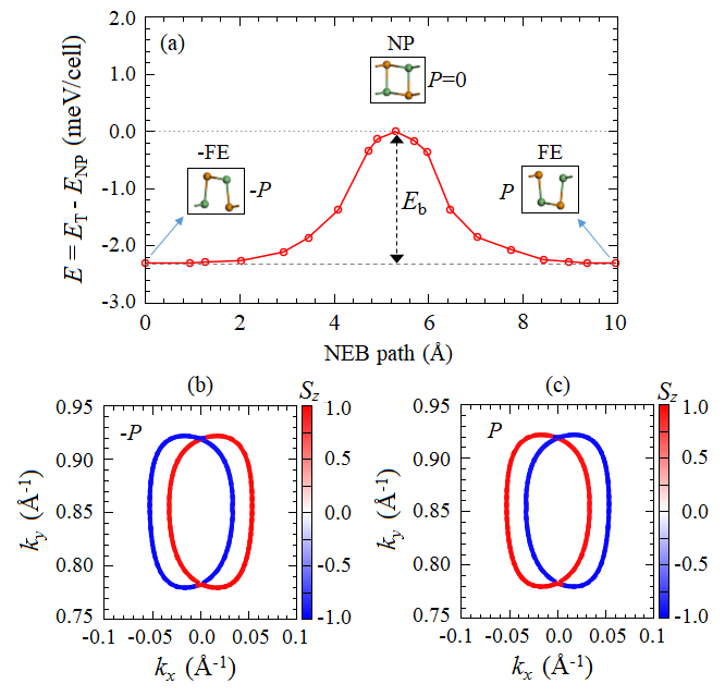
Now, we discuss our prediction of the PSH in correlated to the ferroelectricity in the monolayer. As previously mentioned that the monolayer posses in-plane ferroelectricity Fei et al. (2016); Barraza-Lopez et al. (2018); Kaloni et al. (2019); Wan et al. (2017); Hanakata et al. (2016), which is induced by the in-plane atomic distortion in the real space of the crystal [see Fig. 1(a)]. Therefore, a substantial electric polarization in the in-plane direction is established. For instant, our Berry phase calculation King-Smith and Vanderbilt (1993) on SnTe monolayer revealed that the magnitude of the in-plane electric polarization is 13.8 when an effective thickness of 1 nm for monolayer is used, which is in a good agreement with previous resultWan et al. (2017). Importantly, we predict the feasibility of polarization switching in SnTe monolayer by analyzing the minimum energy pathway of ferroelectric transition calculated using NEB method Henkelman and Jónsson (2000). As shown in Fig. 6(a), we find that the calculated barrier energy for polarization switching process is 2.26 meV/cell in SnTe monolayer. This value is comparable to those of the 2D ferroelectric reported in previous workFei et al. (2016); Ai et al. (2019), but is much smaller than that in conventional ferroelectric BaTiO3Haeni et al. (2004), suggesting that a switchable in-plane ferroelectric polarization is plausible. In deed, polarization switching in various monolayers by using an external electric field or strain effects has recently been reported Hanakata et al. (2016).
By switching the in-plane ferroelectric polarization in monolayer, e.g., by applying an external electric field, a fully reversal of the out-of-plane spin orientation can be expected. This is due to the fact that switching the in-plane ferroelectric polarization from to is equivalent to the space inversion operation which changes the wave vector from to , but preserves the spin vector Di Sante et al. (2013); Kim et al. (2014). Suppose that is the Bloch state of the crystal with ferroelectric polarization . Under the space inversion operation , both the polarization and the wave vector are reversed so that . However, application of the time reversal symmetry reverses only the , while the remains unchanged, leading to the fact that . The expectation values of spin operator can now be calculated by
| (7) |
which indicates that the spin orientation can be reversed by switching the ferroelectric polarization. This analysis is in fact confirmed by our calculated results of the spin textures shown in Fig. 6(b)-(c), where the fully reversal of the out-of-plane spin orientation is achieved under opposite in-plane ferroelectric polarization. Such an interesting property indicates that an electrically controllable PSH in monolayer can be realized, which is very useful for operation in the spintronic devices.
Thus far, we have predicted that the PSH with large spin splitting is achieved in the monolayer. In particular, GeTe monolayer is promising for spintronics since it has the largest strength of the spin splitting ( eVÅ) among the monolayer. Because the PSH is achieved on the spin-split bands near the VBM [Fig. 3(a)], -type doping for spintronics is expected to be realized. Moreover, by injection the hole doping into the valence band of the monolayer, it is possible to map the formation and evolution of the PSH state using near-filled scanning Kerr microscopyRudge et al. (2015), which allow us to resolve the features down to tens-nm scale with sub-ns time revolution. Finally, the hole-doped monolayer can also be applied to explore current-induced spin polarization known as a Edelstein effectEdelstein (1990) and associated spin-orbit torqueGambardella and Miron (2011), indicating that the present system is promising for spintronic devices.
IV CONCLUSION
In summary, by using first-principles DFT calculations, supplemented with symmetry analyses, we investigated the effect of the SOC on the electronic structures of the monolayer. We found that due to point group symmetry in the monolayer, the unidirectional out-of-plane spin configurations are preserved, inducing the PSH state that is similar to the [110] Dresselhauss model Bernevig et al. (2006) observed on the [110]-oriented semiconductor QW. Our first-principle calculations on various (: Sn, Ge; : S, Se, Te) monolayers confirmed that this PSH is observed at near the VBM, supporting large spin splitting and small wavelength of the spin polarization. More importantly, we observed a reversible out-of-plane spin orientations under opposite in-plane ferroelectric polarization, indicating that an electrically controllable PSH in monolayer can be realized, which is promising for spintronic devices.
Recently, there are a number of other 2D materials that are predicted to maintain the in-plane ferroelectricity and the symmetry of the crystals. Therefore, it opens a possibility to further explore the achievable PSH states in these materials. Among them are coming from the 2D elemental group‐V (As, Sb, and Bi) monolayer with the puckered lattice structure Xiao et al. (2018); Liu et al. (2019). Therefore, it is expected that our predictions will stimulate further theoretical and experimental efforts in the exploration of the PSH state in the 2D-based ferroelectric materials, broadening the range of the 2D materials for future spintronic applications.
Acknowledgements.
The first author (M.A.U. Absor) would like to thanks Nanomaterial Reserach Institute, Kanazawa University, Japan, for providing financial support during his research visit. This work was partly supported by Grants-in-Aid on Scientific Research (Grant No. 16K04875) from the Japan Society for the Promotion of Science (JSPS) and a JSPS Grant-in-Aid for Scientific Research on Innovative Areas ”Discrete Geometric Analysis for Materials Design” (Grant No. 18H04481). Part of this research was supported by PDUPT Research Grant (2019) and BOPTN Research Grant (2019), Universitas Gadjah Mada, Indonesia.References
- Nitta et al. (1997) J. Nitta, T. Akazaki, H. Takayanagi, and T. Enoki, Phys. Rev. Lett. 78, 1335 (1997).
- Manchon et al. (2015) A. Manchon, H. C. Koo, J. Nitta, S. M. Frolov, and R. A. Duine, Nat. Matter 14, 871 (2015).
- Dresselhaus (1955) G. Dresselhaus, Phys. Rev. 100, 580 (1955).
- Rashba (1960) E. I. Rashba, Sov. Phys. Solid State 2, 1224 (1960).
- Kuhlen et al. (2012) S. Kuhlen, K. Schmalbuch, M. Hagedorn, P. Schlammes, M. Patt, M. Lepsa, G. Güntherodt, and B. Beschoten, Phys. Rev. Lett. 109, 146603 (2012).
- Qi et al. (2006) X.-L. Qi, Y.-S. Wu, and S.-C. Zhang, Phys. Rev. B 74, 085308 (2006).
- Ganichev et al. (2002) S. D. Ganichev, E. L. Ivchenko, V. V. Bel’kov, S. A. Tarasenko, M. Sollinger, D. Weiss, W. Wegscheider, and W. Prettl, Nature 417, 153 (2002).
- Lu et al. (1998) J. P. Lu, J. B. Yau, S. P. Shukla, M. Shayegan, L. Wissinger, U. Rössler, and R. Winkler, Phys. Rev. Lett. 81, 1282 (1998).
- Datta and Das (1990) S. Datta and B. Das, Appl. Phys. Lett. 56, 665 (1990).
- Chuang et al. (2009) P. Chuang, S.-H. Ho, L. W. Smith, F. Sfigakis, M. Pepper, C.-H. Chen, J.-C. Fan, J. P. Griffiths, I. Farrer, H. E. Beere, G. A. C. Jones, D. A. Ritchie, and T.-M. Chen, Nature Nanotechnology 10, 35 (2009).
- Dyakonov and Perel (1972) M. I. Dyakonov and V. I. Perel, Sov. Phys. Solid State 13, 3023 (1972).
- Bernevig et al. (2006) B. A. Bernevig, J. Orenstein, and S.-C. Zhang, Phys. Rev. Lett. 97, 236601 (2006).
- Schliemann (2017) J. Schliemann, Rev. Mod. Phys. 89, 011001 (2017).
- Altmann et al. (2014) P. Altmann, M. P. Walser, C. Reichl, W. Wegscheider, and G. Salis, Phys. Rev. B 90, 201306 (2014).
- Koralek et al. (2009) J. D. Koralek, C. P. Weber, J. Orenstein, B. A. Bernevig, S.-C. Zhang, S. Mack, and D. D. Awschalom, Nature 458, 610 (2009).
- Walser et al. (2012) M. P. Walser, C. Reichl, W. egscheider, and G. Salis, Nature Physics 8, 757 (2012).
- Schönhuber et al. (2014) C. Schönhuber, M. P. Walser, G. Salis, C. Reichl, W. Wegscheider, T. Korn, and C. Schüller, Phys. Rev. B 89, 085406 (2014).
- Ishihara et al. (2014) J. Ishihara, Y. Ohno, and H. Ohno, Applied Physics Express 7, 013001 (2014).
- Kohda et al. (2012) M. Kohda, V. Lechner, Y. Kunihashi, T. Dollinger, P. Olbrich, C. Schönhuber, I. Caspers, V. V. Bel’kov, L. E. Golub, D. Weiss, K. Richter, J. Nitta, and S. D. Ganichev, Phys. Rev. B 86, 081306 (2012).
- Sasaki et al. (2014) A. Sasaki, S. Nonaka, Y. Kunihashi, M. Kohda, T. Bauernfeind, T. Dollinger, K. ARichter, and J. Nitta, Nature Nanotechnology 9, 703 (2014).
- Chen et al. (2014) Y. S. Chen, S. Fält, W. Wegscheider, and G. Salis, Phys. Rev. B 90, 121304 (2014).
- Yamaguchi and Ishii (2017) N. Yamaguchi and F. Ishii, Applied Physics Express 10, 123003 (2017).
- Absor et al. (2015) M. A. U. Absor, F. Ishii, H. Kotaka, and M. Saito, Applied Physics Express 8, 073006 (2015).
- Absor and Ishii (2019) M. A. U. Absor and F. Ishii, Phys. Rev. B 99, 075136 (2019).
- Ai et al. (2019) H. Ai, X. Ma, X. Shao, W. Li, and M. Zhao, Phys. Rev. Materials 3, 054407 (2019).
- Fei et al. (2016) R. Fei, W. Kang, and L. Yang, Phys. Rev. Lett. 117, 097601 (2016).
- Barraza-Lopez et al. (2018) S. Barraza-Lopez, T. P. Kaloni, S. P. Poudel, and P. Kumar, Phys. Rev. B 97, 024110 (2018).
- Kaloni et al. (2019) T. P. Kaloni, K. Chang, B. J. Miller, Q.-K. Xue, X. Chen, S.-H. Ji, S. S. P. Parkin, and S. Barraza-Lopez, Phys. Rev. B 99, 134108 (2019).
- Wan et al. (2017) W. Wan, C. Liu, W. Xiao, and Y. Yao, Applied Physics Letters 111, 132904 (2017), https://doi.org/10.1063/1.4996171 .
- Hanakata et al. (2016) P. Z. Hanakata, A. Carvalho, D. K. Campbell, and H. S. Park, Phys. Rev. B 94, 035304 (2016).
- Perdew et al. (1996) J. P. Perdew, K. Burke, and M. Ernzerhof, Phys. Rev. Lett. 77, 3865 (1996).
- Ozaki et al. (2009) T. Ozaki, H. Kino, J. Yu, M. J. Han, N. Kobayashi, M. Ohfuti, F. Ishii, T. Ohwaki, H. Weng, and K. Terakura, http://www.openmx-square.org/ (2009).
- Troullier and Martins (1991) N. Troullier and J. L. Martins, Phys. Rev. B 43, 1993 (1991).
- Ozaki (2003) T. Ozaki, Phys. Rev. B 67, 155108 (2003).
- Ozaki and Kino (2004) T. Ozaki and H. Kino, Phys. Rev. B 69, 195113 (2004).
- Theurich and Hill (2001) G. Theurich and N. A. Hill, Phys. Rev. B 64, 073106 (2001).
- Absor et al. (2018a) M. A. U. Absor, I. Santoso, Harsojo, K. Abraha, H. Kotaka, F. Ishii, and M. Saito, Phys. Rev. B 97, 205138 (2018a).
- Absor et al. (2016) M. A. U. Absor, H. Kotaka, F. Ishii, and M. Saito, Phys. Rev. B 94, 115131 (2016).
- Absor et al. (2017) M. A. U. Absor, I. Santoso, Harsojo, K. Abraha, H. Kotaka, F. Ishii, and M. Saito, Journal of Applied Physics 122, 153905 (2017).
- Absor et al. (2018b) M. A. U. Absor, H. Kotaka, F. Ishii, and M. Saito, Japanese Journal of Applied Physics 57, 04FP01 (2018b).
- Gomes and Carvalho (2015) L. C. Gomes and A. Carvalho, Phys. Rev. B 92, 085406 (2015).
- Appelbaum and Li (2016) I. Appelbaum and P. Li, Phys. Rev. B 94, 155124 (2016).
- Henkelman and Jónsson (2000) G. Henkelman and H. Jónsson, The Journal of Chemical Physics 113, 9978 (2000), https://doi.org/10.1063/1.1323224 .
- King-Smith and Vanderbilt (1993) R. D. King-Smith and D. Vanderbilt, Phys. Rev. B 47, 1651 (1993).
- Xu et al. (2017) L. Xu, M. Yang, S. J. Wang, and Y. P. Feng, Phys. Rev. B 95, 235434 (2017).
- Yao et al. (2017) W. Yao, E. Wang, H. Huang, K. Deng, M. Yan, K. Zhang, K. Miyamoto, T. Okuda, L. Li, Y. Wang, H. Gao, C. Liu, W. duan, and S. Zhou, Nat. Commn. 8, 14216 (2017).
- Liu et al. (2013) Q. Liu, Y. Guo, and A. J. Freeman, Nano Letters 13, 5264 (2013), pMID: 24127876.
- Singh and Romero (2017) S. Singh and A. H. Romero, Phys. Rev. B 95, 165444 (2017).
- Tao and Tsymbal (2018) L. L. Tao and E. Y. Tsymbal, Nature Communications 9, 2763 (2018).
- Fiori et al. (2014) G. Fiori, F. Bonaccorso, G. Iannaccone, T. Palacios, D. Neumaier, A. Seabaugh, S. K. Banerjee, and L. Colombo, Nature Nanotechnology 83, 768 (2014).
- Haeni et al. (2004) J. H. Haeni, P. Irvin, W. Chang, R. Uecker, P. Reiche, Y. L. Li, S. Choudhury, W. Tian, M. E. Hawley, B. Craigo, A. K. Tagantsev, X. Q. Pan, S. K. Streiffer, L. Q. Chen, S. W. Kirchoefer, L. J., and D. G. Schlom, Nature 430, 758 (2004).
- Di Sante et al. (2013) D. Di Sante, P. Barone, R. Bertacco, and S. Picozzi, Advanced Materials 25, 509 (2013), https://onlinelibrary.wiley.com/doi/pdf/10.1002/adma.201203199 .
- Kim et al. (2014) M. Kim, J. Im, A. J. Freeman, J. Ihm, and H. Jin, Proceedings of the National Academy of Sciences 111, 6900 (2014), https://www.pnas.org/content/111/19/6900.full.pdf .
- Rudge et al. (2015) J. Rudge, H. Xu, J. Kolthammer, Y. K. Hong, and B. C. Choi, Review of Scientific Instruments 86, 023703 (2015), https://doi.org/10.1063/1.4907712 .
- Edelstein (1990) V. Edelstein, Solid State Communications 73, 233 (1990).
- Gambardella and Miron (2011) P. Gambardella and I. M. Miron, Philosophical Transactions of the Royal Society A: Mathematical, Physical and Engineering Sciences 369, 3175 (2011), https://royalsocietypublishing.org/doi/pdf/10.1098/rsta.2010.0336 .
- Xiao et al. (2018) C. Xiao, F. Wang, S. A. Yang, Y. Lu, Y. Feng, and S. Zhang, Advanced Functional Materials 28, 1707383 (2018), https://onlinelibrary.wiley.com/doi/pdf/10.1002/adfm.201707383 .
- Liu et al. (2019) B. Liu, M. Niu, J. Fu, Z. Xi, M. Lei, and R. Quhe, Phys. Rev. Materials 3, 054002 (2019).