Electrostatic responses of anisotropic dielectric films
Abstract
We study the electrostatic responses (i.e. retardation effects due to the propagation of electromagnetic waves are ignored) of a linear homogeneous and anisotropic (LHA) dielectric film to an arbitrary external electrostatic potential, which may be generated by charges located either inside or outside it. A formalism is developed to calculate the polarization charges induced in the film. In our derivation, the idea is exploited that a physical boundary can be looked upon as a region of rapid variation in polarization rather than a simple geometric separation. With this no boundary conditions are needed in solving the relevant electrostatics problem. Our approach makes it clear that the responses consist of two contributions, one arising from the very presence of surfaces while the other existing even in an infinite medium. The approach can be applied not just to electrostatic but also many problems and is of great pedagogical value. In light of the results, we discuss graphene plasma waves under the influence of a LHA dielectric film such as a few-layer hexagonal boron nitride. It is found that the dispersion of these waves is strongly affected by the anisotropy at wavelengths comparable to the film thickness.
I introduction
As well known in electrostatics, an exterior probe charge cannot induce volume polarization charges in a linear homogeneous and isotropic (LHI) dielectric, as the divergence of the displacement field and hence that of the electric field – which is proportional to in a LHI – vanish in the body. Polarization charges appear only where inhomogeneity exists, e.g. at the interfaces and surfaces adjoining two LHI media. In the traditional textbook approach of evaluating the amount of polarization charges on the surface of – for instance – a semi-infinite medium (SIM), the electrostatic fields residing on the opposite sides of the surface are treated separately on a piece-wise homogeneity basis and then joined by a set of boundary conditions requiring the continuity of the normal component of and that of the electrostatic potential at the surface. landauEM In this approach, a surface is more of a geometric separation rather than a physical entity.
The purpose of the present work is two-fold. First, we exploit an alternative approach for studying the electrostatic responses of dielectrics. In this new approach, an interface is treated, as in an atomistic approach, as a physical region over which electric polarization undergoes rapid variation. Though atomistically unknown a priori, such variations can be fixed on a macroscopic scale by which the interfacial region appears infinitely thin. As a result, boundary conditions are done away with in totality. It should be mentioned that this macroscopic description of surfaces has recently been employed in the study of surface plasma waves, deng2017 ; deng2019 ; deng2018 i.e. electron density ripples propagating on the surface of conductors. Similar ideas have been used in a very different context, i.e. the study of plasma waves in bounded two-dimensional electron gas. fetter
Second, we apply the approach to study the responses of linear homogeneous anisotropic (LHA) dielectric films. While the electrostatics of LHI media make a standard part of any textbook on electromagnetism, LHA media have been unduly less exposed despite the fact that the latter constitute a big portion in real life. Existing work on LHA dielectrics have been focused on SIMs and often in a geophysical context. li1997 ; mele2001 However, in the world of nanometer electronics, one has to deal with LHA dielectrics of nanometric thickness. It is therefore desirable to conduct a systematic exposition of the electrostatic responses of LHA films and clarify the thickness effects. Differing from a LHI dielectric, a LHA dielectric can host both volume and boundary polarization charges, which can vary significantly depending on the film thickness. We derive and solve a set of algebraic equations for determining the responses of a LHA film to an arbitrary external potential, which might be generated by probe charges located inside or outside the film. With the results we examine the polarization charges induced in a film by a point charge. Two cases are considered, corresponding to the point charge being located inside and outside the film, respectively. As an additional example, we employ the results to discuss the behaviors of plasma waves in a mono-layer graphene under the influence of a LHA film such as a few-layer hexagonal boron nitride. These materials belong to the family of the so-called van der Waals materials, which are a hot topic in contemporary research. vdW We find that the plasma wave dispersion is strongly affected by the anisotropy at wavelengths comparable to the film thickness.
II Macroscopic description of an interface
From an atomistic point of view, an interface is not just a geometric separation but a physical region in which the polarization rapidly evolves from one side to the other. For the sake of illustration, let us imagine bringing in touch two semi-infinite dielectrics, A and B, and an atomically thin interface forms amid them. We shall assume that the interface is macroscopically flat and extends within the plane so that its normal points along -direction, see Fig. 1. The polarization in the entire space is denoted by , where denotes a point in the space with being the planar projection. Quite generally, far away from the interface, we expect that takes on the bulk value on the A/B side. As one moves across the interface from A to B, shall evolve from to . One may introduce an evolution function , which approaches unity for lying deeply in A whereas it approaches zero for lying deeply in B. Then, . The exact form of in the interfacial region depends on atomistic details. Nevertheless, on the macroscopic scale by which the interfacial region appears infinitely thin, one can approximate by the Heaviside step function regardless of the atomistic details, presuming that the surface be located at without loss of generality. As such, the macroscopic description of an interface is fixed in a fairly generic manner. deng2019 In the case of a SIM, we have B as the vacuum and A as the medium. With and writing simply as , we can write
| (1) |
Note that equation (1) gives the polarization in the entire system (the dielectric plus the vacuum) and hence no boundary is needed in this global view. The polarization charge density is then obtained as
| (2) |
where is the density of volume charges in the dielectric and gives the density of charges existing on the surface. Here and represents a point on the surface.
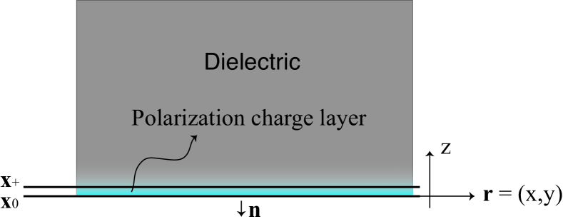
As an illustration of the usefulness of Eq. (2), let us consider a LHI characterized by a constant susceptibility , i.e. . Assuming no interior probe charges, i.e. for lying inside the medium and hence , we find from Eq. (2) that , where is the dielectric constant. As expected, is concentrated on the surface. To bring the expression into the familiar form, let us note that , where with being the positive infinitesimal (see Fig. 1 for illustration). See that and represent points on the planes sandwiching the polarization charge layer, as shown in Fig. 1. Now we obtain , which implies an areal density of , where is the unit vector pointing along the outward normal of the surface, as expected of the traditional approach.
III Responses of LHA dielectric films
The dielectric film under consideration has two infinitely extended flat surfaces at and , respectively. It is characterized by a constant susceptibility tensor of the following diagonal form,
This is not the most general form but captures the properties of a large variety of materials including van der Waals materials. It shall prove convenient to introduce the dielectric tensor components as and , together with the anisotropy parameter . We can write and , where .
In analogy with Eq. (1), the global polarization in this system can be written as
| (3) |
where with . The polarization charge density then reads
| (4) |
Here the first term, which vanishes in a LHI but not in a LHA, gives the density of volume charges while the second one gives the density of surface charges.
We introduce the planar Fourier transform pair for a field quantity ,
where is the wave vector along the surface. As our system is linear, it suffices to consider one Fourier component, say . Subsequently, we shall suppress the index and write simply as , which should not be confused with as their arguments are of different character. Equation (4) is then rewritten
| (5) |
where is confined to the dielectric and .
Our task is to calculate induced by an external probe potential , which is supposed to be generated by a charge of density . The electrostatic potential due to is denoted by . It is well known and can be easily shown that
| (6) |
Here and the zero point of the potential has been set at infinity.
III.1 General formalism
Note that , where and, as mentioned earlier, is the total electrostatic potential. Substituting this in Eq. (5) yields
| (7) |
where
| (8) |
is the charge density that exists also in an infinite medium and
| (9) |
denotes the charge density purely due to the presence of surfaces. It should be clear that, Eqs. (6) - (9) make a closed set and can be solved already to determine the polarization charges. Below we prescribe them in a more tractable way.
To make progress, we extend in the following cosine series,
| (10) |
where and with being zero unless . It shall prove convenient to split into a symmetric part and an anti-symmetric part , where collects all the terms with even and those with odd . Obviously, is symmetric about the mid-plane of the film while is anti-symmetric. In terms of , one can recast
| (11) |
for lying in the dielectric. It follows that takes on the following values at the surfaces,
| (12) |
Now we have .
Let for . We can write as a linear function of , i.e. , where the matrix elements can be established from Eq. (11) as
| (13) |
From Eq. (8) we obtain
| (14) |
Analogously, from Eq. (9) it follows that
| (15) |
Adding Eqs. (14) and (15), one ends up with a linear inhomogeneous algebraic equation for , which can then be solved for any .
It is interesting to note that, due to the factor appearing in both and , the symmetric sector and the anti-symmetric sector are actually decoupled. As such, we can deal with them separately. To this end, let us define and with being an integer. It immediately follows that
| (16) |
where the matrix is given by
| (17) |
Similarly, we have
| (18) |
where the matrix is given by
| (19) |
These algebraic equations (16) - (19) fully determine the electrostatic responses of the film.
The solutions to the above equations are readily to be found. Formally, they can be written as
| (20) |
where is independent of and , given by
| (21) |
Further manipulations show that
| (22) |
The expressions relevant for are analogous. For the sake of completeness, they are written down as follows
| (23) | |||||
| (24) | |||||
| (25) |
Equations. (22) and (25) represent the key results of this paper, which can be used to calculate the polarization charges for any given . The expressions of imply that there are two general contributions to the polarization charges. deng2018 One of these contains . This contribution exists only in the presence of the surfaces. The other is directly due to and exists even if there is no surface.
We point out that and can be written in terms of . Actually, and can be obtained from Eq. (12) with in place of . It is worth noting that
| (26) |
More precisely, , and only involves whereas only involves . These properties ensure that a (anti-) symmetric only induces a (anti-) symmetric , in accord with the symmetry of the system.
III.2 The limit
Suppose is very small so that does not vary much across the film and . Then one may retain only the term for , i.e. . The total volume charges then amounts to . This approximation, however, does not apply to , which is localized and must have all terms present. It is thus useful to construct a separate formalism for this special case. By Eq. (8), we arrive at
| (27) |
From Eq. (6) one can show that
| (28) |
where and are the areal density of polarization charges localized on the surface and , respectively. Substituting this expression in Eq. (27) leads to
| (29) |
On using the following relations
| (30) |
we obtain
| (31) | |||||
| (32) |
where . Now Eqs. (29), (31) and (32) make a closed set of algebraic equations and can be solved to get and . Clearly, only is involved.
Here are some general observations based on these equations. Firstly, by Eq. (29), we see that
where ”” represents higher-order terms in . This means that the total volume charges are proportional to the total probe charges residing in the film to the lowest order in . If all probe charges are located outside, volume charges can be neglected for thin films, in which circumstances one obtains from Eqs. (31) and (32) that
Secondly, Eqs. (31) and (32) suggest that
If the probe charges are symmetrically distributed, i.e. , the amounts of charges on the surfaces are equal and of the same sign, as expected of the reflection symmetry and in line with the general formalism set out in Sec. III.1.
III.3 The semi-infinite limit
For , for all and the two surfaces are decoupled. The responses then reduce to that of a SIM. Now one notes that and degenerate to , where
| (33) |
where . Adding Eq. (16) to Eq. (18), we find
| (34) |
where we have defined
The sum over in Eq. (33) can be converted into an integral as are densely distributed for large . Identifying , and with and , respectively, as well as with so that , we find
| (35) |
Here
is independent of . Now Eq. (34) can be manipulated to obtain
| (36) |
where the source reads
| (37) |
Here and . Multiplying Eq. (36) by and integrating it over , we arrive at
| (38) |
where we have used the following integral that can be easily evaluated by the method of contour integration
| (39) |
Equations (36) - (38) completely determine the response of a semi-infinite LHA dielectric.
These equations can be modified to describe the responses of an infinite medium without any surfaces. In the latter case, the term with – which arises only due to surfaces – does not exist in the expression of , Eq. (36), and the term with does not exist in either, Eq. (37). An alternative rational leading to this modification goes by assuming that the probe charges be placed far from the surfaces so that vanishes near the surfaces and that one looks only at the polarization charges far from the surfaces, so that the contribution from the term with , which decays away from the surfaces, can be neglected. Then one finds
for an infinite medium.
In the isotropic case with and , it follows from Eq. (36) that and
where
It is useful to write , with and stemming from the first and the second term of , respectively. It is easy to show that
which is the only contribution if the probe charges are located outside the film (i.e. ). As is independent of , its leads to charges localized on the surface, the areal density of which can be shown to be . This result is of course well known. As for , it contributes to the surface charges but also volume charges, the latter amounting to , which is nothing but the polarization charge that would exist in an infinite medium, see above. The total charges in the volume then is , as expected.
IV Examples
IV.1 A point charge outside the film
Let us consider a point probe charge of strength placed at , a distance of exterior to the surface at . It follows that ,
| (40) |
and
| (41) |
With these expressions we find
| (42) |
as well as
| (43) |
which can be inserted in Eqs. (20) - (25) to obtain
| (44) |
and analogously
| (45) |
For large , .
To obtain some analytical insight, let us look at the SIM limit. Equation (41) then transforms into the following
| (46) |
Substituting this into Eq. (37) yields
| (47) |
With this we get from Eqs. (36) and (38) that
| (48) |
In the isotropic limit this reduces to discussed in Sec. III.3. The corresponding electrostatic potential is
| (49) |
which is the same as would be produced by a fictitious point charge – the image charge – of value located at .
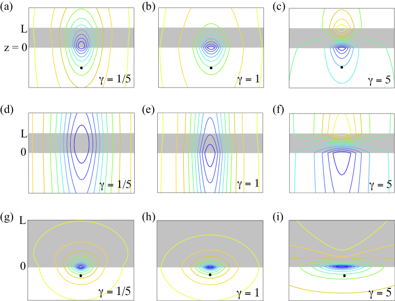
In Fig. 2 is displayed the equipotentials of , i.e. the potential produced by the polarization charges only, for a variety of situations specified by and . A black dot indicates the position of the point probe charge . We calculate the contour lines by . Considering that for a point charge actually depends only on the magnitude of not its direction, we can rewrite this expression as , where is the zeroth order Bessel function of the first kind. In the numerical calculation, we have replaced upper bound of the integral by a cut-off . Physically, this means the probe charge is smeared over an area rather than being ideally point-like, i.e. . Only in the limit does this expression represent an ideal point charge. We observe several features worth attention. Firstly, for , as seen in panels (c), (f) and (i), the polarization charges are mostly concentrated near the surfaces, regardless of . For larger , these charges appear on both surfaces, while for smaller , they are more concentrated on the surface closer to the probe charge. Secondly, for , a significant amount of volume charges appear though only if , as seen in panels (a), (d) and (g). Thirdly, in the isotropic case, , polarization charges are concentrated on the surface closer to the probe charge regardless of .
IV.2 A point charge inside the film
Now let us suppose that the point probe charge is located at inside the film, for which and
| (50) |
as well as
| (51) |
It follows that
| (52) |
and
| (53) |
These sources are then used to to obtain via Eqs. (20) - (25). In contrast with the case of the probe charge being outside, here are not simply proportional to due to the cosine terms in the latter.
Again we consider the SIM limit to obtain some analytical results. Now
| (54) |
With this we obtain
| (55) |
This expression is very similar to the source in the case of the probe charge outside film, Eq. (47), but with the crucial difference of its dependence via the factor . Now we find
| (56) |
together with
| (57) |
The electrostatic potential generated by can again be written as
| (58) |
which is of the same form as Eq. (49). This potential could be produced by two fictitious point charges located beneath the surface. As can be rewritten as , one may say that the first fictitious charge is located at of strength while the other at of strength . It is interesting to note that, outside the film the first charge exactly cancels the potential generated by the probe charge.
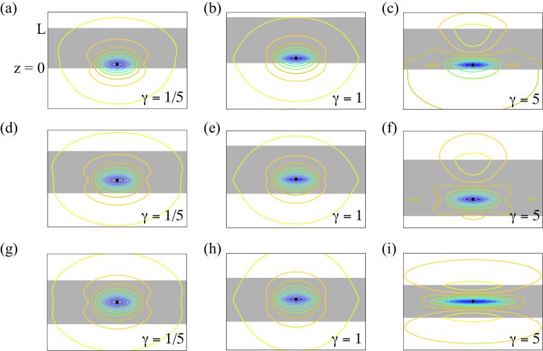
In Fig. 3 we illustrate the electrostatic potential generated by the polarization charges. As in Fig. 2, the probe charge, located at inside the film and indicated by a black dot, is not ideally point-like but smeared over an area of with . In comparison with the case of an exterior probe charge (Fig. 2), here the polarization charges are all concentrated where the probe charge is located regardless of as long as . For , two additional features are observed. Firstly, volume charges appear also elsewhere not just about the probe charge, as inferred from the contour lines not enclosing the probe charge. Secondly, charges also appear on the surfaces.
IV.3 Plasma waves in graphene
The last example discussed here concerns plasma waves in graphene – an atomically thin sheet of carbon atoms sitting on a honeycomb lattice. Plasma waves, which are propagating electron density ripples, in this quasi-two–dimensional world has caused a big stir in the filed of plasmonics. GrPW As a result of the low dimensionality, the properties of these waves are highly liable to its dielectric environment.
Let us consider the simplest case of a plane charge density wave traveling within a graphene layer placed at , a distance of over a LHA dielectric film. Here , which plays the role of , denotes the charge density at point in the layer and moment , while and are the wave vector and frequency of the wave, respectively. The latter obey a dispersion relation governed by an equation that can be shown of the following form in the electrostatic limit if the electronic collisions in the graphene layer can be neglected, deng2015
| (59) |
where – which might depend on – is the bare electrical conductivity of the graphene layer and is the electrostatic potential at this layer. Now contains two contributions, one from the charges of density carried by the plasma waves and the other from the polarization charges of density induced by in the dielectric underneath. The former is simply . The latter can be written as where
| (60) |
does not depend on . Combined, they yield
| (61) |
We may interpret as the effective dielectric function felt by the charges in graphene. This is plugged in Eq. (59) to produce
| (62) |
which determines the dispersion of the plasma waves. The frequency is reduced in the long wavelength limit () but not much altered in the short wavelength limit ().
In the limit , one finds , implying that a semi-infinite LHA medium effects as a LHI medium with dielectric constant , as expected from Eq. (48). In the limit , as shown in Sec. III.2, volume charges can be neglected in the dielectric. From the results established in Sec. III.2, it follows that This expression shows that the correction due to a thin dielectric is typically very small unless is close to unity, in which case the effective conductivity might be made to change sign and no plasma waves would then exist (i.e. would become imaginary). The wave frequency would be widely tunable in such case by varying .
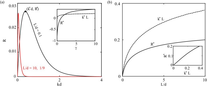
For simplicity, let us use a Drude model for graphene conductivity and write , where is a real-valued parameter that can be tuned by doping. Then, one finds with . We wish to elucidate the effects of anisotropy on as a function of . To this end, we calculate the ratio , where denotes the frequency had the dielectric been an LHI (also of thickness ) with the dielectric constant . The results are displayed in Fig. 4 (a) for two values of , where we see that reaches a peak at . The inset in panel (a) shows that, while increases with increasing , only weakly depends on . On the other hand, as shown in Fig. 4 (b), both and strongly depend on . The former increases while the latter decreases as increases. Further, as shown in the inset of (b), we note that , where is a function of .
The above results may be used in the measurement of the anisotropy parameter of a LHA. One may first measure out the dispersion covering both the regimes of and . Then can be inferred from this measured in the limit . With , can then be computed, which can be used to obtain . This method can be very accurate, because can be very large depending on . For the example shown in Fig. 4 (b), reaches for and can be increased further with thicker films.
V Conclusions
To summarize, we have presented a formalism for calculating the electrostatic responses, i.e. retardation effects excluded, of a LHA film with a diagonal but anisotropic susceptibility tensor. Generalization to an arbitrary tensor is straightforward but not included in this work. The most interesting aspect of our derivation is that, a generic macroscopic physical description of surfaces is prescribed, which does away with the boundary conditions that are essential in traditional textbook approaches. Our formalism makes it clear that the responses consist of two contributions, one stemming from the very presence of surfaces while the other existing even in an infinite medium. We have illustrated the formalism with three examples. In one of these we discuss the plasma waves in graphene under the influence of a LHA film. It is shown that the frequency of the waves is strongly affected at wavelength comparable to the film thickness.
While we explicitly speak of a dielectric, our formalism can be equally applied to calculate the electrical responses (e.g. current flow) in an anisotropic conductor by the duality relation that exists between conductivity tensor and susceptibility tensor.
References
- (1) L. D. Landau and E. M. Lifshitz, Electrodynamics of continuous media (Elsevier Science, New York, 1940).
- (2) H.-Y. Deng, K. Wakabayashi and C.-H. Lam, ”Universal self-amplification channel for surface plasma waves,” Phys. Rev. B 95, 045428 - 045437 (2017); H.-Y. Deng, ”Theory of nonretarded ballistic surface plasma waves in metal films,” Phys. Rev. B 95, 125442 - 125454 (2017).
- (3) H.-Y. Deng, ”A universal macroscopic theory of surface plasma waves and their losses,” New J. Phys. 21, 043055 - 043074 (2019).
- (4) H.-Y. Deng, ”An Analytical Dynamical Response Theory for Bounded Medium Without Additional Boundary Conditions: A Unified Perspective of Common Models,” Arxiv 1806.08308 (2018).
- (5) A. L. Fetter, ”Edge magnetoplasmons in a two-dimensional electron fluid confined to a half-plane,” Phys. Rev. B 33, 3717 - 3723 (1986).
- (6) P. Li and N. F. Uren, ”Analytical solution for the point source potential in an anisotropic 3-D half-space I: Two-Horizontal-Layer case,” Mathl. Comput. Modelling 26, 9 - 27 (1997).
- (7) E. J. Mele, ”Screening of a point charge by an anisotropic medium: anamorphoses in the method of images,” Am. J. Phys. 69, 557 - 562 (2001).
- (8) K. S. Novoselov, A. Mishchenko, A. Carvalho and A. H. Castro Neto, ”2D materials and van der Waals heterostructures,” Science 353, 6298 - 6308 (2016).
- (9) A. N. Grigorenko, M. Polini and K. S. Novoselov, ”Graphene plasmonics,” Nat. Photonics 6, 749 - 758 (2012).
- (10) H.-Y. Deng and K. Wakabayashi, ”Retardation effects on plasma waves in graphene, topological insulators, and quantum wires,” Phys. Rev. B 92, 045434 - 045441 (2015). Equation (59) can be rewritten as , where is the bare density-density response function of graphene. Further, since , one may write so that the equation becomes , which is the more often adopted version of Eq. (62). Obviously, .
- (11) J. P. Wait, ”Current flow into a three dimensional anisotropic conductor,” Radio Sci. 25, 689 - 694 (1990).