Stochastic Sparse Learning with Momentum Adaptation for Imprecise Memristor Networks ††thanks: Y. Wang and S. Wu contribute equally to this work. Corresponding to: lpshi@mail.tsinghua.edu.cn
Abstract
Memristor based neural networks have great potentials in on-chip neuromorphic computing systems due to the fast computation and low-energy consumption. However, the imprecise properties of existing memristor devices generally result in catastrophic failures for the network in-situ training, which significantly impedes their engineering applications. In this work, we design a novel learning scheme that integrates stochastic sparse updating with momentum adaption (SSM) to efficiently train the imprecise memristor networks with high classification accuracy. The SSM scheme consists of: (1) a stochastic and discrete learning method to make weight updates sparse; (2) a momentum based gradient algorithm to eliminate training noises and distill robust updates; (3) a network re-initialization method to mitigate the device-to-device variation; (4) an update compensation strategy to further stabilize the weight programming process. With the SSM scheme, experiments show that the classification accuracy on multilayer perceptron (MLP) and convolutional neural network (CNN) improves from 26.12% to 90.07% and from 65.98% to 92.38%, respectively. Meanwhile, the total numbers of weight updating pulses decrease 90% and 40% in MLP and CNN, respectively, and the convergence rates are both 3 faster. The SSM scheme provides a high-accuracy, low-power, and fast-convergence solution for the in-situ training of imprecise memristor networks, which is crucial to future neuromorphic intelligence systems.
Index Terms:
memristors, neural networks, crossbar, momentum, neuromorphicI Introduction
Recently, the field of neuromorphic computing has witnessed substantial advances in artificial intelligence applications achieved by deep neural networks (DNNs), such as image classification [1], speech recognition [2] and game playing [3]. DNNs gain powerful generalization capabilities by their massive tunable weights, which are such data-intensive that the computation efficiency is usually limited by the memory access. Some DNN accelerators [4] and neuromorphic chips [5, 6] are designed with application-specific integrated circuit (ASIC) to alleviate the memory access bottleneck to speed up the computation. However, the synaptic weights are still stored in random access memories (RAM) rather than directly encoded by the states of emerging analogue devices. Such analogue device assembled systems are believed to achieve significant speedup and power reduction for on-chip deployments of DNNs [7].
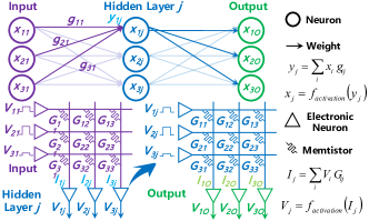
One of the most attractive devices is two-terminal memristor, which offers the advantages of high density, fast speed and low-power consumption [8]. The conductance of a memristor can be programmed by update voltage pulses or read by low-amplitude reading voltage pulses [9]. Therefore, the weights in memristor based neural networks could be accessed and tuned locally, which is extremely suitable for the DNN hardware representation. As shown in Figure 1, when implemented in the crossbar structure, memristor arrays are ideal substrates that directly perform multiply-accumulate operations (MACs) at the weight locations. This parallel computing character speeds up the training and inference of DNNs with very low-energy consumption, providing promising computing paradigm for neuromorphic computing systems [7, 8, 9].
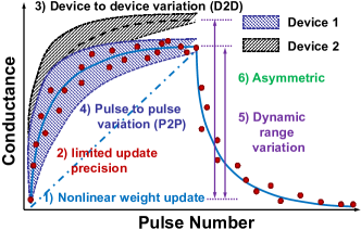
From engineering design perspective, ideal characteristics, including low variability, stable analogue conductance levels and linear updating behaviors, are desired for synaptic memristor devices [10]. However, existing memristor devices have substantial non-ideal characteristics (Figure 2) [11], such as device-to-device (D2D) variation, pulse-to-pulse (P2P) variation, dynamic range (on/off ratio) variation, and reading noises, which lead to the imprecise encoding of network weights and the corresponding computation. The conductance of memristors is usually determined by the formation and rupture of conductive filaments, which is a relatively stochastic process [12]. Thus, these non-ideal properties are natural and cannot be eliminated at least in the near future. Besides, the updating process of the conductance is nonlinear, asymmetric, and limited-precision (caused by discrete pulse width) [11]. These properties discussed above generally lead to non-convergence when training real memristor neural networks.
It is highly desirable to explore an effective solution for the in-situ training on imprecise memristor networks. To this end, we design an efficient and general in-situ training solution for imprecise memristor neuromorphic systems. Our contributions are twofold: (1) We build a simulator to quantitatively analyze the effects of various characteristics in memristor based networks. The simulator supports various neural network models and is easy to be inserted into deep learning frameworks. We find that the accuracy degradation is mainly caused by the non-reading updating scheme, pulse width precision, and the D2D variation. (2) We propose a learning scheme that integrates stochastic sparse updating with momentum adaption (SSM) to significantly improve the accuracy and learning efficiency of imprecise memristor networks. The effectiveness of our SSM scheme is demonstrated on various networks and datasets. For MLP on MNIST [13] dataset, the network accuracy improves from 26.12% to 90.07%, and the number of updating pulses decreases 90%. For CNN on Fashion [14] dataset, the network accuracy improves from 65.98% to 92.38%, and the number of updating pulses decreases 40%. Meanwhile, the convergence rates of the MLP and the CNN are both 3 faster.
II Related work
In previous studies, learning schemes that consider all of the non-ideal memristor network properties were rarely reported. The reports of multiple devices for each synaptic weight [15] and additional random sparse adaption (RSA) network [16] were proposed to alleviate the effects of D2D variations. However, these designs increase the circuit overheads and hinder the network size. Some complicated programming schemes were also proposed to improve the precision of weight updates, such as non-identical programming pulses scheme [17] and closed-loop update scheme [18]. However, the non-identical programming pulses scheme could not be applied with the parallel weight updating method [19], which significantly increases the training latency. The closed-loop update scheme needs several programming cycles to approach the target precision, which extremely increases the number of updating pulses and leads to high latency and energy consumption. Moreover, both schemes need a (or several) read step(s) before weight programming, which inevitably complicate the peripheral circuitry design. A threshold weight update scheme was also proposed to suppress the effects of nonlinear weight changing [20], while other memristor characteristics were not considered, such as the variation of D2D and P2P.
III Device model
Memristors are usually metal-insulator-metal structured with two-terminals. Their conductance is generally determined by the filaments formed by active metal atoms or oxygen vacancies [12], as shown in Figure 3a. The number of the filaments or, equivalently, the area covered by the filaments inside a memristor can be tuned by the external electric field, thus the conductance (weight) of a memristor could be programmed by voltage pulses. In this work, we use a state parameter to describe the area covered by filaments in memristors. The dynamic change of in response to the external voltage is modeled by Equation 1, which is verified by the experimental data [21]:
| (1) |
Where the , , are positive parameters determined by the material of memristors, is the ion hopping distance, and are the hopping barrier heights.
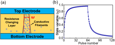
In Equation 1, the exponential dependence dynamic of and allows memristors to be read at a low amplitude pulse (e.g., bellow 0.1V), which negligibly disturbs their states (the is small). On the other hand, using high amplitude pulses will program the of the device. During programming process, the potentiation pulses or depression pulses are identical with fixed amplitudes (/) and widths (/), which makes the training process simple and suitable for engineering purpose (Table I). However, as shown in Figure 3b, the trade-off is that the device state changes in a nonlinear and discrete (limited pulse width precision) manner. The current through the memristor can be modeled [21] by
| (2) |
Where , , , are positive parameters determined by the material, is the effective tunneling distance, is the tunneling barrier, is the depletion width of the Schottky barrier region and the is the Schottky barrier height. The details of parameters used in the model are shown in Table I.
In Equation 2, the voltage and current of a memristor is approximately linear-correlated at low voltage (e.g., bellow 0.1V), then the reading conductance is approximately a constant. Thus we chose the reading voltage as 0.05V and the input voltage during learning is below 0.1V.
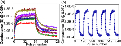
For real memristors, due to fabrication nuances, the conductance update behaviors are different among different devices. To quantify this D2D variation, we assume that the initial parameters in Equations 1 and 2 of different devices vary according to Gaussian distributions [21, 22]. The mean values and standard deviations of each parameter are shown in Table I. The standard deviation of each parameter is represented as a percentage of its mean value. Besides the D2D variation, P2P variation is also an important non-ideal property of real memristors. To quantify the P2P variation, we assume that P2P variation is 10% of the D2D variation. Because of the variations derived from D2D and P2P, the dynamic range (on/off ratio) between maximum and minimum conductance of each device also differs. Figure 4 shows the simulation results with all non-ideal characteristics under voltage pulses.
| Param | mean | std | Param | mean | std | Param | value |
|---|---|---|---|---|---|---|---|
| 1e-4 | 3% | 0.5 | 3% | -1.1V | |||
| 19.25 | 3% | 1.58e-3 | 15% | 3 µs | |||
| 13 | 3% | 0.5 | 3% | 1.4V | |||
| 3.01e-3 | 10% | 0.05V | - | 30 µs |
IV Non-ideal effects on memristor networks
IV-A Simulator for Non-ideal Memristor Networks
As shown in Figure 1, since MACs can be directly mapped into memristor networks, both the forward and backward process can be performed directly by hardware memristor networks. To quantify the effects of the non-ideal characteristics, we build a one-to-one correspondent simulator based on TensorFlow [23] for representations of memristor networks and evaluations of their performances. The general dataflow during the simulation is shown in Figure 5.

In our simulation, the parameters of each memristor are defined as collections and their mean values are defined as (Table I). For the network initialization, the of each memristor among the network are according to a Gaussian distribution. In this condition, each device has its own parameters , where and denotes the row and column index in memristor array. Although the initial is same for each device (0.5), individual leads to an approximate Gaussian distribution of the initial conductance among all memristors. The input vector is mapped into the amplitude of the voltage pulse by
| (3) |
Since is normalized to , the , which ensures that negligibly disturbs the state of the memristor. The current collected at the output of each column in the network array can be obtained as:
| (4) |
where the parameters are the of each memristor.
For the hardware representation of MACs, the elements values of a matrix , which represent the weights of the network synapses, are mapped into the conductance values of the memristor:
| (5) | ||||
Where and are mean values of maximum and minimum conductance. Since the properties of each memristor are not expected to be measured during the mapping, all parameters in Equation 5 are the mean values of memristor array, i.e., in Table I. Then MACs are executed and the output results should be mapped by the current:
| (6) |
For multi-layer networks, we continue the inference process until the final output layer and calculate the training error. Through the naive error back-propagation algorithm in TensorFlow, the weight update value corresponding to the mapped for each memristor is calculated. Once obtaining , the programming pulse time can be calculated. Our simulator has two types weight updating scheme: open-loop and closed-loop. In order to reduce the complexity of peripheral circuits, latency and energy overheads, memristors are expected to be tuned in an open-loop scheme without reading their states:
| (7) |
where is an amplification coefficient. In previous studies [24], is generally set as the pulse number required to switch the memristor between minimum and maximum conductance, e.g., 64. For real memristor systems, the programming pulse number should be rounded because of the fixed programming pulse width.
On the other hand, the closed-loop scheme provides a relatively precise updating. In our simulation configuration, the closed-loop updating requires just one reading step before programming to check the memristor conductance :
| (8) |
The state of the memristor is
| (9) |
The expected update state of the memristor is:
| (10) |
Therefore, the programming pulse time can be obtained as
| (11) | ||||
It should be pointed out that, due to the reading step, the parameters in Equation 8 is the of each memristor. As for the next Equations 9-11, the parameters are the mean value of each parameter in Table I due to the fact that the properties of each memristor are not measured during learning.
Finally, the memristors are programmed by the voltage pulses. The dynamics of the memristor are determined by Equation 1. To introduce the P2P variation into the model, the parameters of one memristor randomly change under a Gaussian distribution before each pulse.
IV-B Ablation Studies of Non-Ideal Characteristics
We test the aforementioned simulator with various optional characteristics in real memristor-based MLP and CNN. The MLP has a 3-layer structure with 784 input neurons, 256 hidden neurons and 10 output neurons. The CNN has a LeNet-5 structure [13] with two convolution layers and two fully-connected layers. We use the MNIST and Fashion datasets to test the network performance of MLP and CNN, respectively.
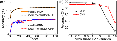
Because of the on/off ratio of memristors, the weight values mapped by them are also limited. In our model, the expectations of maximum and minimum conductance are mapped into the weight +1 and -1 (Equation 5), respectively. While for vanilla networks based on software platform, the synaptic weight have no range limitation. We evaluate the effects of limited weight range on the non-variation memristor network. In this condition, the variation of D2D and P2P are ignored so that the mapped weights only range in [-1, +1], and the weight update scheme is closed-loop. As shown in Figure 6a, ablation experiments indicate that the range limitation has little effect on the network performance for both MLP and CNN.
For the P2P variation, we chose the parameters in Table I as a baseline (existing devices), and zoomed them exponentially to study the effects on the network. In this condition, the weight update scheme is closed-loop and the variation of D2D is ignored. As shown in Figure 6b, the MLP can tolerate up to 2 P2P variation baseline and the CNN can tolerate up to 5. This is contributed to the high robustness of neural networks. We conclude that the single P2P variation is not a major factor for the memristor network accuracy degradation.
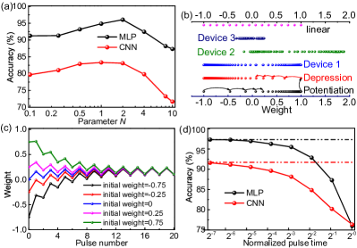
For practical online learning applications of memristor networks, an open-loop weight update scheme is much more attractive than the closed-loop scheme due to its non-reading and fast update properties. We studied the effect of the update coefficient on the network performance in the open-loop scheme. In this condition, the update pulses are rounded to integral numbers, and the variation of D2D and P2P are ignored. As shown in Figure 7a, the results show that a relatively small (e.g., 2) can improve the accuracy in both MLP and CNN, rather than setting it as the pulse number required to switch the memristor between the minimum and maximum conductance (e.g., 64). Through Equation 7, we find that coefficient plays a similar role as the learning rate during training. Like the learning rate, an overlarge may lead to an unstable training process or even non-convergence. On the other hand, a local minimum result occurs if is too small, which is also undesirable for the network performance. Meanwhile, the network accuracy still decays by a large margin even after the optimization. This is due to the inaccurate updates during the open-loop scheme, especially when applying the pulse number rounding. As shown in Figure 7b, due to the discrete pulse number, the impact of a depression (potentiation) pulse is widely different from a potentiation (depression) one at the maximum (minimum) conductance. This asymmetric behavior is further detailed in Figure 7c, where the weight decays towards a center value under identical alternating potentiation and depression pulses. This nonlinear and asymmetric weight update properties seriously degrade the accuracy of the network. A shorter programming pulse width () can reduce this effect. We chose the pulse widths in Table I as a baseline (existing devices, in Figure 7d), and narrowed them exponentially to study the effects on the network. As shown in Figure 7d, a shorter pulse width results in a higher accuracy. However, if the programming pulse is too short, the state of a memristor would not change, which is called the delay time [8]. Thus, the pulse width is not supposed to be less than that in baseline.
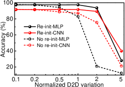
For the D2D variation, we chose 10% of the D2D variation in Table I as a baseline (existing devices), and exponentially zoomed them to study the effects on the network. In this condition, the weight update scheme is closed-loop and the variation of P2P is ignored. As shown in Figure 8, both the MLP and the CNN exhibit tolerances to the D2D variation, which are weaker than the P2P variation in Figure 6b. We find that the accuracy degradation is mainly caused by the weight initialization, which is crucial for training DNNs [25]. D2D variation broadens initial weight distribution, thus resulting in an improper starting point of the network training. To eliminate this effect, we design a re-initialization method (see Section V-A). With the re-initialization, both the MLP and the CNN can be further enhanced to tolerate up to 2 D2D variation baseline. However, if the D2D is too large (e.g., 5 D2D variation baseline), the network accuracy would also be significantly declining. Since the D2D variation of existing devices is close to the baseline, our re- initialization method is powerful enough.
Considering all the non-ideal characteristics discussed above, the network accuracy decreases to extremely low levels or even non-convergence: 26.12% for MLP and 65.98% for CNN. As summarized in Table II, through the comparisons of accuracy drops in the above ablation studies, we conclude that the degradation in real imprecise memristor networks is caused by three major factors: the open-loop update scheme, the pulse width precision, and the D2D variation.
| Variation | Open -loop | Roun ding | Test accuracy (%) | Comment | ||
| P2P | D2D | MLP | CNN | |||
| 97.44 | 91.66 | vanilla | ||||
| 97.34 | 91.71 | ideal | ||||
| ✓ | 97.43 | 91.64 | tolerant | |||
| ✓ | 82.93 | 86.99 | major factors | |||
| ✓ | 96.05 | 83.09 | ||||
| ✓ | 75.96 | 76.32 | ||||
| ✓ | ✓ | ✓ | ✓ | 26.12 | 65.98 | non-ideal |
V Stochastic sparse learning with momentum adaptation (SSM)
Based on the simulation results, we design an SSM scheme to address these issues in the non-ideal memristor network training and enable the network to converge with high performance. The SSM scheme are decomposed as follows.
V-A Re-initialization
A suitable uniform or Gaussian weight initialization with proper variation is benefit for the neural network forward and backward propagation. Thus, we design a simple re-initialization method to reduce the effect of the D2D variation on the network initialization, as shown in Table III.
| 1 | Read memristor conductance , map it to network weight . | |
|---|---|---|
| 2 | Gaussian re-initialization: if apply a depression pulse else apply a potentiation pulse | Uniform re-initialization: is the boundary (e.g., 0.1) if apply a depression pulse else if apply a potentiation pulse |
| 3 | Read and calculate the standard deviation of all synaptic weights. | |
| 4 | Repeat 2 and 3 until suitable standard deviation occurs. | |
V-B Momentum Based Gradient Method
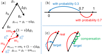
Due to the non-ideal characteristics of memristor networks, training based on the naive stochastic gradient descent (SGD) usually leads to non-convergence. Therefore, we introduce a momentum into the SGD, named as momentum-based SGD (m-SGD) [1] in the SSM scheme. As shown in Figure 9a, each synaptic cell keeps an exponentially weighed average of all previous gradients during training, such that:
| (12) | ||||
Where is the learning rate, is the momentum coefficient defined in . This averaged gradient update can smooth the weight evolution process by filtering out harmful noises that contains little information during one iteration, and distills robust updates that indicate the right directions, which leads to faster and better convergence during training.
V-C Stochastic Rounding Method
When the is small, e.g., 2, as suggested by the experiment results in Figure 7a, the programming pulse number for each cell in one iteration is scaled to a small order of magnitude, e.g., and later smoothed by momentum . Then the pulse width is usually too narrow for practical implementation. In the SSM scheme, as shown in Figure 9b, we apply a stochastic rounding method with {0, 1} to quantize the pulse number [26], otherwise a deterministic rounding will always result in zero pulse:
| (13) |
Where denotes the probability of applying one update pulse on the memristor. The small order of magnitude makes the update number extremely sparse, where only relatively significant weight update can affect a pulse during training.
V-D Compensation Update Method
To further mitigate the asymmetric update behavior and improve the precision of the weight update, a compensation method is designed when weights are near the maximum or minimum conductance (Figure 9c). The current state , the expected update state of the memristor and the can be calculated by Equations 9-11. Then the compensation programming pulse time can be obtained as:
| (14) | ||||
Obviously, the trade-off is that the compensation needs extra pulses and at least one read operation to calculate its number. Therefore, the compensation method is optional in SSM when the application requires higher accuracy.
VI Result and discussion
VI-A Performance of the Re-initialization Method
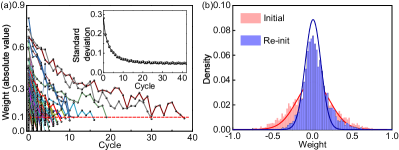
As shown in Figure 10, by our re-initialization, the conductance of the memristor network can be tuned to a suitable narrow deviation within 40 cycles for both uniform and Gaussian scheme. And the average pulse number applied on each cell is about 4. These results indicate that the re-initialization is fast and energy-efficient, and the effects of the D2D variation can be mitigated (Figure 8).
VI-B Performance of SSM the Scheme for MLP and CNN
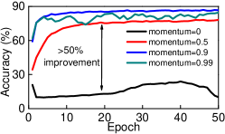
SSM significantly improves the network online learning, as shown in Figure 11. With all of the memristor non-ideal characteristics, the network cannot converge (black line), while the network can quickly converge to a high accuracy (87.18%) with SSM scheme and a suitable momentum coefficient (blue line). We also find that an overlarge (e.g. 0.99) might make the training process unstable and decrease the performance, which has similar phenomenon as the update coefficient . The accuracy can further improve to 90.07% if compensation is applied (Table IV).
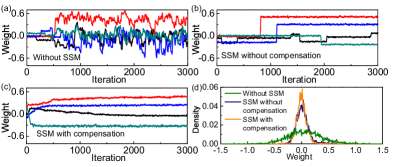
We also extract typical synaptic weight update evolutions during training to visualize the role of the SSM scheme. As shown in Figure 12a, without SSM scheme, even though small updates (noises) can be cleared by the deterministic pulse rounding, the evolution of the weight still fluctuates seriously and leads to an extreme unstable training of the network. We believe this phenomenon is caused by the temporary and local learning information that is constantly changing in each iteration, which contains little explicit direction. As shown in Figure 12b, we find that the SSM scheme with a suitable momentum can obviously decrease the programming pulses for each cell during training. Statistical results of the first 5 epochs, which contains most update events, show that less than 1% of cells are updated in one iteration. In the following epochs, very few devices need to be tuned. This sparse update can highly decrease the energy consumption, as well as stabilize the training and improve the final accuracy (Figure 11). This is due to the fact that SSM scheme can distill robust updates from temporary information in one iteration and indicate the right directions of updating, which leads to a faster and better convergence.
Due to the limited pulse width precision, the synaptic weight still changes sharply at the update point (Figure 12b), which usually indicates an imprecise updating and may hurt the overall network performance. As shown in Figure 12c, with the compensation update method, the weight changes more precisely and smoothly during training, which can further improve the network performance at the cost of reading operations and more pulses.
As shown in Figure 12d, we see that without the SSM scheme, the distribution of the weight after learning is dispersed, while the SSM scheme can narrow the weight distribution and avoid the non-convergence. All of these behaviors discussed above are also verified in the CNN training.
We summarize performance details of MLP and CNN network with the SSM scheme in Table IV. With the SSM scheme, the classification accuracy increases from 26.12% to 87.18% in MLP, and the programming pulse number in the first 5 epochs decreases 90%. As for the CNN, the classification accuracy increases from 65.98% to 90.99%, and the programming pulse number decreases 40%. The convergence rates of MLP and CNN are both 3 times faster. When the compensation method is applied, the classification accuracy can further reach to 90.07% and 92.38% for MLP and CNN, respectively, while the pulse number still approximates to that without the SSM scheme. Therefore, we conclude that our SSM scheme can significantly improve the performance of non-ideal memristor network.
| Scheme | Accuracy (%) | Pulse count* | Epoch | |
| M L P | No SSM | 26.12 | 1 | 25 |
| SSM without compensation | 87.18 | 0.1 | 8 | |
| SSM with compensation | 90.07 | 0.8 | ||
| C N N | No SSM | 65.98 | 1 | 50 |
| SSM without compensation | 90.99 | 0.6 | 16 | |
| SSM with compensation | 92.38 | 1.1 | ||
| *The pulse counts are normalized by the value of no-SSM scheme. | ||||
VI-C Performance of the Compensation Update Method
We evaluated the performance of the compensation update method for different values by stochastically choosing 1000 depression and potentiation weights. The range of is . And the range of the update weight is , which covers most conditions during the network learning.
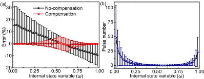
As shown in Figure 13, with the compensation, the average error of the weight update is reduced and the update precision is improved. At the maximum or minimum conductance condition ( or ), the number of compensation pulse is much higher due to the asymmetric update behaviors of the device: when the weight is near maximum (or minimum), a depression (or potentiation) update pulse significantly decreases (or increases) the weight, while a potentiation (or depression) compensation pulse does not change the weight much. Although this large number compensation improves the precise of the weight updating, the trade-off is that the energy cost and the delay time are significantly increased, thus the compensation method is suitable for the application that is insensitive for the efficiency but demands for the high accuracy.
VI-D Prospects of the SSM Scheme
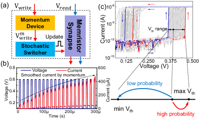
The SSM scheme can be constructed not only by CMOS, such as field programmable gate array (FPGA) and the ASIC chip, but also has great potentials to be implemented by two types of emerging nano-electronic devices, as shown in Figure 14. Recently, an exponentially conductance change characteristic is found in some memristors with short-term plasticity, such as the diffusive memristors, where the momentum can be mimicked. And the stochastic rounding behavior can be also accomplished by the volatile threshold switching selector devices, due to their variation of the threshold voltage.
VII Conclusion
In this work, we quantitatively analysis effects of various non-ideal characteristics in real memristor network on the performance of MLP and CNN. Meanwhile, based on the ablation studies, we design a novel SSM scheme to train the non-ideal memristor based neural network. Impressive classification accuracy is obtained with fewer epochs and programming pluses during the in-situ learning. The simulation results indicate that the SSM scheme promises a fast and low-power in-situ training solution for non-ideal memristor networks in-situ learning, which is an essential step to apply real memristor networks to practical applications.
Acknowledgments
This work is supported by National Nature Science Foundation of China (Nos. 61327902 and 61836004), Suzhou-Tsinghua innovation leading program (No. 2016SZ0102) and Brain-Science Special Program of Beijing under Grant Z181100001518006
References
- [1] A. Krizhevsky, I. Sutskever, and G. E. Hinton, “Imagenet classification with deep convolutional neural networks,” in NIPS, 2012, pp. 1097–1105.
- [2] G. Hinton, L. Deng, D. Yu, G. Dahl, A.-r. Mohamed, N. Jaitly, A. Senior, V. Vanhoucke, P. Nguyen, B. Kingsbury et al., “Deep neural networks for acoustic modeling in speech recognition,” IEEE Signal processing magazine, vol. 29, 2012.
- [3] D. Silver, J. Schrittwieser, K. Simonyan, I. Antonoglou, A. Huang, A. Guez, T. Hubert, L. Baker, M. Lai, A. Bolton et al., “Mastering the game of go without human knowledge,” Nature, vol. 550, no. 7676, p. 354, 2017.
- [4] Y.-H. Chen, T. Krishna, J. S. Emer, and V. Sze, “Eyeriss: An energy-efficient reconfigurable accelerator for deep convolutional neural networks,” IEEE Journal of Solid-State Circuits, vol. 52, no. 1, pp. 127–138, 2017.
- [5] P. A. Merolla, J. V. Arthur, R. Alvarez-Icaza, A. S. Cassidy, J. Sawada, F. Akopyan, B. L. Jackson, N. Imam, C. Guo, Y. Nakamura et al., “A million spiking-neuron integrated circuit with a scalable communication network and interface,” Science, vol. 345, no. 6197, pp. 668–673, 2014.
- [6] L. Shi, J. Pei, N. Deng, D. Wang, L. Deng, Y. Wang, Y. Zhang, F. Chen, M. Zhao, S. Song et al., “Development of a neuromorphic computing system,” in IEDM. IEEE, 2015, pp. 4–3.
- [7] P. Yao, H. Wu, B. Gao, S. B. Eryilmaz, X. Huang, W. Zhang, Q. Zhang, N. Deng, L. Shi, H.-S. P. Wong et al., “Face classification using electronic synapses,” Nature communications, vol. 8, p. 15199, 2017.
- [8] M. A. Zidan, J. P. Strachan, and W. D. Lu, “The future of electronics based on memristive systems,” Nature Electronics, vol. 1, no. 1, p. 22, 2018.
- [9] C. Li, M. Hu, Y. Li, H. Jiang, N. Ge, E. Montgomery, J. Zhang, W. Song, N. Dávila, C. E. Graves et al., “Analogue signal and image processing with large memristor crossbars,” Nature Electronics, vol. 1, no. 1, p. 52, 2018.
- [10] S. Yu, “Neuro-inspired computing with emerging nonvolatile memorys,” Proceedings of the IEEE, vol. 106, no. 2, pp. 260–285, 2018.
- [11] P.-Y. Chen, X. Peng, and S. Yu, “Neurosim+: An integrated device-to-algorithm framework for benchmarking synaptic devices and array architectures,” in IEDM. IEEE, 2017, pp. 6–1.
- [12] J. J. Yang, D. B. Strukov, and D. R. Stewart, “Memristive devices for computing,” Nature nanotechnology, vol. 8, no. 1, p. 13, 2013.
- [13] Y. LeCun, L. Bottou, Y. Bengio, P. Haffner et al., “Gradient-based learning applied to document recognition,” Proceedings of the IEEE, vol. 86, no. 11, pp. 2278–2324, 1998.
- [14] H. Xiao, K. Rasul, and R. Vollgraf, “Fashion-mnist: a novel image dataset for benchmarking machine learning algorithms,” arXiv preprint arXiv:1708.07747, 2017.
- [15] S. Yu, P.-Y. Chen, Y. Cao, L. Xia, Y. Wang, and H. Wu, “Scaling-up resistive synaptic arrays for neuro-inspired architecture: Challenges and prospect,” in IEDM. IEEE, 2015, pp. 17–3.
- [16] A. Mohanty, X. Du, P.-Y. Chen, J.-s. Seo, S. Yu, and Y. Cao, “Random sparse adaptation for accurate inference with inaccurate multi-level rram arrays,” in IEDM. IEEE, 2017, pp. 6–3.
- [17] P.-Y. Chen, B. Lin, I. Wang, T.-H. Hou, J. Ye, S. Vrudhula, J.-s. Seo, Y. Cao, S. Yu et al., “Mitigating effects of non-ideal synaptic device characteristics for on-chip learning,” in ICCAD. IEEE Press, 2015, pp. 194–199.
- [18] M. Hu, C. E. Graves, C. Li, Y. Li, N. Ge, E. Montgomery, N. Davila, H. Jiang, R. S. Williams, J. J. Yang et al., “Memristor-based analog computation and neural network classification with a dot product engine,” Advanced Materials, vol. 30, no. 9, p. 1705914, 2018.
- [19] P.-Y. Chen, D. Kadetotad, Z. Xu, A. Mohanty, B. Lin, J. Ye, S. Vrudhula, J.-s. Seo, Y. Cao, and S. Yu, “Technology-design co-optimization of resistive cross-point array for accelerating learning algorithms on chip,” in DATE. EDA Consortium, 2015, pp. 854–859.
- [20] C.-C. Chang, P.-C. Chen, T. Chou, I.-T. Wang, B. Hudec, C.-C. Chang, C.-M. Tsai, T.-S. Chang, and T.-H. Hou, “Mitigating asymmetric nonlinear weight update effects in hardware neural network based on analog resistive synapse,” IEEE Journal on Emerging and Selected Topics in Circuits and Systems, vol. 8, no. 1, pp. 116–124, 2018.
- [21] S. Choi, P. Sheridan, and W. D. Lu, “Data clustering using memristor networks,” Scientific reports, vol. 5, p. 10492, 2015.
- [22] P. M. Sheridan, F. Cai, C. Du, W. Ma, Z. Zhang, and W. D. Lu, “Sparse coding with memristor networks,” Nature nanotechnology, vol. 12, no. 8, p. 784, 2017.
- [23] M. Abadi, P. Barham, J. Chen, Z. Chen, A. Davis, J. Dean, M. Devin, S. Ghemawat, G. Irving, M. Isard et al., “Tensorflow: A system for large-scale machine learning,” in OSDI, 2016, pp. 265–283.
- [24] S. Agarwal, S. J. Plimpton, D. R. Hughart, A. H. Hsia, I. Richter, J. A. Cox, C. D. James, and M. J. Marinella, “Resistive memory device requirements for a neural algorithm accelerator,” in IJCNN. IEEE, 2016, pp. 929–938.
- [25] D. Mishkin and J. Matas, “All you need is a good init,” arXiv preprint arXiv:1511.06422, 2015.
- [26] S. Wu, G. Li, F. Chen, and L. Shi, “Training and inference with integers in deep neural networks,” ICLR, 2018.