Carrier Recombination Mechanism at Defects in Wide Bandgap Two-dimensional Materials from First-principles
Abstract
Identification and design of defects in two-dimensional (2D) materials as promising single photon emitters (SPE) requires a deep understanding of underlying carrier recombination mechanisms. Yet, the dominant mechanism of carrier recombination at defects in 2D materials has not been well understood, and some outstanding questions remain: How do recombination processes at defects differ between 2D and 3D systems? What factors determine defects in 2D materials as excellent SPE at room temperature? In order to address these questions, we developed first-principles methods to accurately calculate the radiative and non-radiative recombination rates at defects in 2D materials, using -BN as a prototypical example. We reveal the carrier recombination mechanism at defects in 2D materials being mostly dominated by defect-defect state recombination in contrast to defect-bulk state recombination in most 3D semiconductors. In particular, we disentangle the non-radiative recombination mechanism into key physical quantities: zero-phonon line (ZPL) and Huang-Rhys factor. At the end, we identified strain can effectively tune the electron-phonon coupling at defect centers and drastically change non-radiative recombination rates. Our theoretical development serves as a general platform for understanding carrier recombination at defects in 2D materials, while providing pathways for engineering of quantum efficiency of SPE.
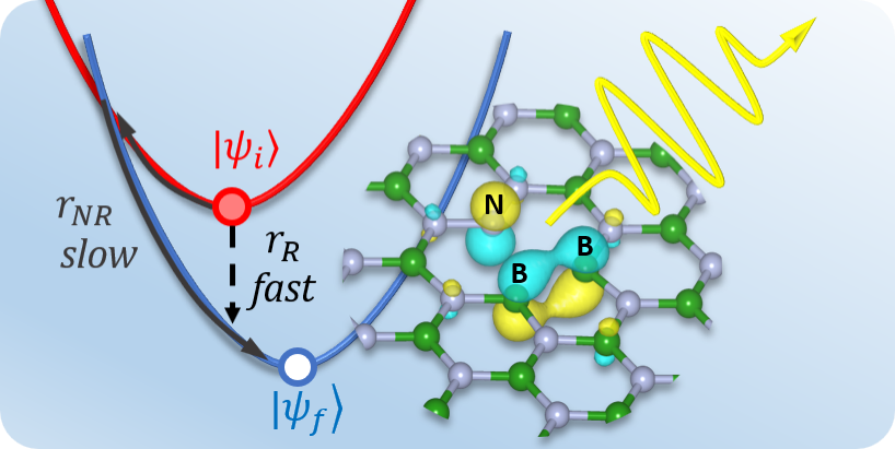
The engineering of spin defects in wide-band semiconductors offers a promising avenue for the development of quantum spin devices. Aharonovich et al. (2011); Ladd et al. (2010); Seo et al. (2016); Dreyer et al. (2018) They are among the few alternatives for quantum technologies that operate at room temperature. Deep defects in two-dimensional (2D) materials such as hexagonal boron nitride (-BN) Aharonovich and Neu (2014); Tran et al. (2016); Kim et al. (2018); Bourrellier et al. (2016); Grosso et al. (2017); Li et al. (2017); Exarhos et al. (2017, 2019); Museur et al. (2008); Sontheimer et al. (2017); Jungwirth et al. (2016); Jungwirth and Fuchs (2017); Noh et al. (2018) and transition metal dichalcogenides (TMD) Mak and Shan (2016); Palacios-Berraquero et al. (2017) have proven to be promising single photon sources with polarized and ultrabright single photon emission at room temperature. These materials exhibit unprecedented potential for several applications, including large-scale nanophotonics and quantum information processing, Beveratos et al. (2002); O’Brien et al. (2009); Scarani et al. (2009); Aharonovich et al. (2016); Vogl et al. (2018) which in turn provide a new platform for exploring quantum phenomena. Dreyer et al. (2018) In order for these defect centers to provide bright SPE, Aharonovich et al. (2011, 2016) the radiative recombination rate (photon emitted) needs to be high, while the non-radiative recombination rate (no photon emitted) must be substantially lower to yield a high quantum efficiency. Furthermore, a weak electron-phonon coupling is also required to ensure long spin relaxation time for the application of qubit and stable single photon emission at room temperature.
Despite the importance of maximizing radiative rates for quantum information, the factors which determine the recombination process at defects in 2D materials are not understood experimentally or theoretically. Past theoretical studies have either focused on radiative recombination in pristine 2D materials Palummo et al. (2015); Wu et al. (2017) or phonon assisted non-radiative recombination for defects in 3D wide band-gap semiconductors. Alkauskas et al. (2014a); Shi et al. (2015) Therefore, a fully comparative study of both recombination processes for defect centers in 2D materials is highly desired.
Furthermore, the high tunability of SPE allows them to be integrated within a vast array of applications. Tran et al. (2016); Aharonovich et al. (2016) Among these methods, strain modulation is one of the most effective strategies, especially for low-dimensional materials which can work under large distortion. Brawand et al. (2015) For example, in 2D systems, some key electronic properties such as band gap, change by 1.5% under 1% uniaxial tension in TMD monolayers Chang et al. (2013) or 6% under 1% uniaxial tension in phosphorenePeng et al. (2014). Additionally, the non-radiative process, which is intrinsically sensitive to lattice deformation (as it is phonon mediated), may exhibit even more drastic changes under strain.
In this communication, we first introduce the formalism of computing the radiative and non-radiative lifetime of defect excited states from first-principles. We then focus on comparing radiative and non-radiative processes of different transitions in a series of important defects in monolayer -BN, where we discuss the dominant recombination processes and their implication on SPE efficiency. Finally, we show that applying strain to -BN defects can effectively tune the non-radiative rates and quantum yield of SPE.
The radiative and non-radiative transition rates between two electronic states under perturbation can be computed via Fermi’s golden rule:
| (1) | ||||
| (2) |
Here, and denote the recombination rates between electronic states and via a radiative process () and non-radiative process (), respectively. is the degeneracy factor of the final state, i.e. several equivalent energy-degenerate atomic configurations of the final state might exist. Alkauskas et al. (2014b) For defects in 2D materials studied in this work, factors are all equal to 1. is the electron-photon coupling (electromagnetic) Hamiltonian and is the electron-phonon coupling Hamiltonian. A sum over phonon states enters the non-radiative recombination process with an occupation number of the vibronic state . For ground state calculations, we employed open source plane-wave code Quantum ESPRESSO Giannozzi et al. (2009) with ONCV norm conserving pseudopotentials Hamann (2013); Schlipf and Gygi (2015) and a supercell size of or higher. Charge corrections for the total energies and eigenvalues of charged defects were applied by employing the techniques developed in Ref. 26; 36. The total energies, defect formation energies and geometry were computed at both PBE and hybrid functional levels (the results presented in the main text are computed at PBE, and detailed comparison between two levels can be found in the Supporting Information (SI) Table S4). The band gaps of pristine -BN are computed at as done in our previous work Wu et al. (2017), which are 6.01 eV for bulk and 7.01 eV for monolayer -BN respectively. The exciton dipole moments and exciton energies as input for radiative lifetime were computed at many body perturbation theory with GW approximation for quasiparticle energies Govoni and Galli (2015); Ping et al. (2013); Nguyen et al. (2012) and then solving the Bethe-Salpeter equation with the Yambo-code Marini et al. (2009), as well as Random Phase approximation with DFT eigenvalues (detailed comparison can be found in the SI, Table S3; the results in the main text are computed at DFT-RPA). More computational details and formulation of radiative rates are discussed in the SI and Ref. 41.
The non-radiative rate is simplified by the static coupling approximation with a one-dimensional (1D) effective phonon approximationAlkauskas et al. (2014a, b); Barmparis et al. (2015); Alkauskas et al. (2012, 2016); Brawand et al. (2015); Giustino (2017); Henry and Lang (1977); Howgate (1969); Monserrat (2018); Pässler (1974, 1976); Shi and Wang (2012); Shi et al. (2015); Wickramaratne et al. (2018); Shi et al. (2018); Yang et al. (2016); Stoneham (2001) (the validation of 1D effective phonon approximation in -BN is based on the similarity of Huang-Rhys factors between 1D effective phonon and all phonon calculations, as discussed in the SI, section IV):
| (3) | ||||
| (4) | ||||
| (5) |
where is naturally separated into an electronic term and a phonon term with temperature dependence from thermal population (). Here is the zero phonon line energy (ZPL), which can be measured experimentally by photoluminescence. We implemented the non-radiative recombination rates as postprocessing codes of Quantum ESPRESSO Giannozzi et al. (2009).
A single defect may introduce several energy levels within the band gap of the host material. This yields the possibility for transitions to occur between defect states (“defect-defect” transition), as well as from a defect state to a band edge (“defect-band” transition). The computed non-radiative lifetimes and capture coefficients of the most probable defect-band transitions for hole captures in multiple defects in monolayer and bulk -BN as well as bulk GaN are listed in Table 1 (where (X=C, O, N) denotes X substitution of boron accompanied by a nitrogen vacancy). The capture coefficients are defined as a product of recombination rates with surface area or volume for 2D or 3D systems, respectively. The corresponding defect formation energies and configuration coordinate diagrams are presented in the SI, Figure S1. We find that all defect-band transitions in monolayer -BN have very small rates (the corresponding lifetime exceeds milliseconds). This is in contrast to typical 3D bulk defects in other materials, such as GaN- or GaN-, where the non-radiative lifetime is at the picosecond level with a similar defect concentration to -BN. Shi and Wang (2012); Alkauskas et al. (2014b); Reshchikov (2014)
| System | ZPL (eV) | (amu1/2Å) | (meV) | (cmn/s) | |
|---|---|---|---|---|---|
| ML (2D) | 5.78 | 0.58 | 86 | ms | |
| ML (2D) | 4.26 | 0.84 | 85 | ms | |
| ML (2D) | 5.46 | 0.51 | 95 | ms | |
| ML (2D) | 3.87 | 0.35 | 150 | ms | |
| Bulk (3D) | 2.69 | 0.35 | 149 | 6.6 s | |
| GaN-(3D) | 1.00 | 1.39 | 39 | * | 0.29 ps |
| ML (2D) | 2.04 | 0.53 | 100 | 102 ps | |
| (defect-defect) |
-
•
* in Ref. 32.
One key reason that non-radiative defect-band recombination in monolayer -BN is typically slow, is due to large energy differences between defect states and band edges ( eV) as the ZPL shown in Table 1. Wu et al. (2017); Smart et al. (2018); Rasmussen et al. (2016) Nonetheless, other factors such as the effective phonon frequencies and the change of nuclear positions can also affect the rates, as discussed later. For example, comparing monolayer BN- with bulk BN-, only the ZPL changes significantly (over 1 eV) and other parameters ( and ) retain nearly constants, which ultimately leads to a two order of magnitude difference in their capture rates. Physically, the phonon-assisted non-radiative rate is dominated by a charge transfer process between initial and final state potential energy surfaces, and can be approximated by a classical Marcus’ theory picture (see Figure 1). Given the form of the energy barrier for charge transferBrawand et al. (2015), a large energy difference between the two states (ZPL) results in an exponential drop in the transfer rate (although exceptions can be found Nan et al. (2009); Jortner (1976); Pässler (1982); Shi et al. (2015)). Therefore, in monolayer -BN, the large ZPLs of defect-band transitions result in extremely slow non-radiative recombination processes (over milliseconds). On the other hand, several defects have allowed defect-defect transitions with viable non-radiative rates due to smaller energy differences, e.g. the (nitrogen substitution of boron accompanied by a nitrogen vacancy) defect-defect transition in monolayer -BN (Table 2).
Hence, the remaining discussions are focused on defect-defect transitions in monolayer -BN. Defect-defect non-radiative recombination is performed for neutral excited and ground state with constrained occupation number. The equilibrium geometry, ZPL and vibrational frequency can be also obtained at DFT with constrained occupation. More computational details for defect-defect nonradiative recombination can be found in SI, section III, Figure S2 and Table S4.
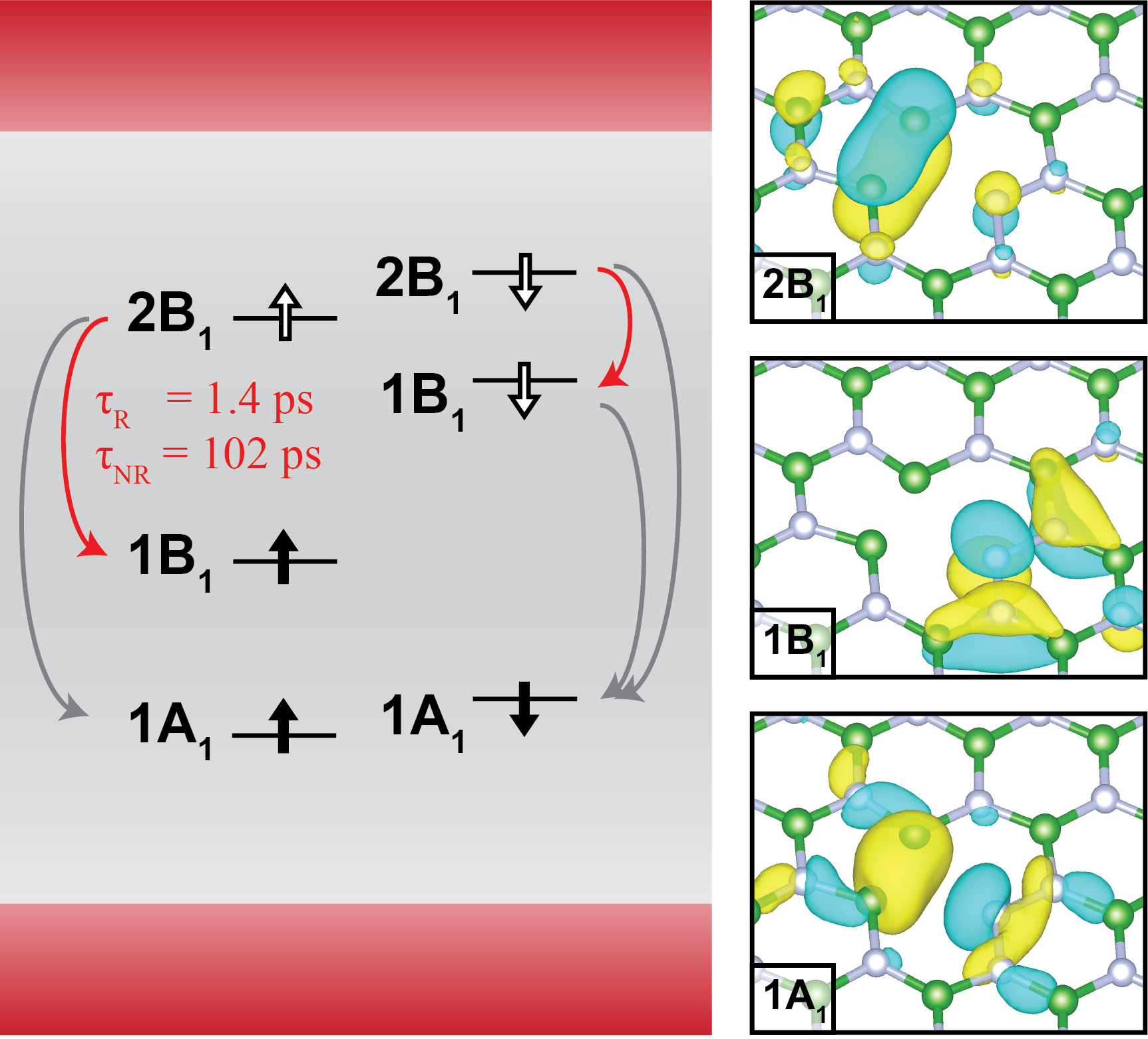
Considering a typical point defect such as which has been proposed as a promising defect for SPE, Exarhos et al. (2019); Tran et al. (2016); Abdi et al. (2018) we find it introduces several isolated energy levels that lead to multiple possible radiative and non-radiative defect-defect recombination pathways (as shown in Figure 2). However, we found only the transition between and (HOMO-LUMO transition for the majority spin channel) has a viably short radiative lifetime and non-radiative lifetime. All other processes have a non-radiative lifetime longer than ms, much slower than this transition which is at a picosecond level.
| Transition | ZPL (eV) | (meV) | * | (cm2/s) | (ps) | |||
|---|---|---|---|---|---|---|---|---|
| / | 2.04 | 100 | 20 | 5.3 | 1.3 | 0.38 | 102 | |
| / | 1.33 | 58 | 23 | 16.6 | ||||
| / | 2.94 | 65 | 46 | 7.8 | ||||
| / | 1.61 | 57 | 28 | 3.2 | 0.03 |
-
•
*
The non-radiative transition rate is determined by multiple factors based on Eq. 3. The first factor is the phonon term . As the ZPL for all defect-defect transitions are relatively small (less than 3 eV, unlike defect-band transitions), we analyze the subtle difference causing variation of among different transitions, based on the relation: where and is the HR factor. Alkauskas et al. (2014b). Specifically ( for all defect-defect transitions we study here), a high implies a large electron-phonon coupling and generally will increase the phonon contribution . For example, the HR factor for the / transition (16.6) is several times larger than other transitions in Table 2 and therefore yields the largest of at 300 K. On the other hand, a high value of means a large energy difference (ZPL) relative to the phonon frequency and will reduce phonon contribution , similar to earlier discussions on defect-band transitions. The second factor is the electronic term , which is proportional to the overlap between electronic wavefunctions . Ultimately, only the / transition has a reasonably large and the largest , which leads to a viable non-radiative recombination process with a lifetime of 102 ps at 300 K.
The radiative process is more straightforward to interpret as it is directly related to the symmetries of wavefunctions via the dipole transition matrix elements . Computational details can be found in section VI and Table S3 in the SI. The corresponding transition section rules for radiative recombination of defect in -BN are listed in Table S5. Both the / transition and the / transition are symmetry allowed,Abdi et al. (2018) resulting in short radiative lifetimes of 1.4 ps and 2.5 ps, respectively. This lifetime can be considered to be a lower-bound compared to that of experimental results, because a much higher defect concentration is adopted in practical calculations (1 defect in a 72-atom supercell, i.e. 1 defect per 2 nm2, compared to order of one SPE per m2 in experiments Tran et al. (2016)) and both radiative and non-radiative lifetimes will increase linearly with decreasing defect concentrations or increasing supercell size (see Ref. 44 and section V Table S1 and S2 in the SI). At the low concentration limit, we can consider the defect acts as an isolated molecule in the 2D planeWu et al. (2019), which gives an upper-bound of the actual lifetime, i.e. 40 ns for / radiative lifetime at . This is in good agreement with the experimental radiative lifetime of monolayer -BN SPE, which are measured to be on the order of ns.Tran et al. (2016); Bourrellier et al. (2016); Grosso et al. (2017); Exarhos et al. (2017) We note that different from the recombination rates, the capture coefficient is generally constant as a function of defect concentration or supercell sizes (see Table S1 and S2 in the SI).
The quantum yield of a SPE (excluding substrate effects) is defined as . Pankove (1975); Chevallier et al. (2017); Hamanaka et al. (2014) By comparing the radiative lifetimes with the non-radiative ones shown in Table 2 for the defect, we have which shows it has the potential to be a highly efficient quantum emitter. In practice, several other external effects can cause the quantum yield to be substantially lower. In particular, substrate recombination Rosenberger et al. (2018), photobleaching Martínez et al. (2016), and strain (discussed in the next section) are known to play the role of limiting the quantum yield of defect SPE.
| Strain | ZPL (eV) | (Å) | (meV) | (ps) | |||
|---|---|---|---|---|---|---|---|
| No strain | 2.04 | 0.666 | 100 | 5.33 | 0.38 | 1.26 | 102 |
| Biaxial | 2.08 | 0.613 | 105 | 4.69 | 0.39 | 0.28 | 429 |
| Biaxial | 2.01 | 0.732 | 96 | 6.18 | 0.36 | 9.20 | 16 |
| Uniaxial | 2.02 | 0.637 | 102 | 4.96 | 0.39 | 0.95 | 127 |
| Uniaxial | 2.07 | 0.703 | 98 | 5.80 | 0.36 | 1.98 | 70 |
| Uniaxial | 2.10 | 0.642 | 103 | 5.05 | 0.38 | 0.38 | 336 |
| Uniaxial | 1.98 | 0.697 | 98 | 5.69 | 0.37 | 5.39 | 25 |
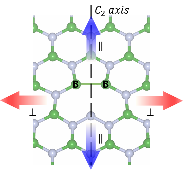
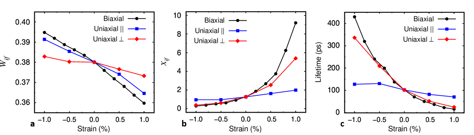
In this work, we discuss the impact of strain on non-radiative recombination (and leave other external effects for future study) with as an example. Presumably, strain will change the radiative lifetime little (orbital overlaps between initial and final states are largely preserved) compared to that of the non-radiative lifetime which can be strongly affected by changes in local structures. As shown in Figure 3, strain may be applied along the symmetry axis (denoted as strain) or orthogonal to the symmetry axis (denoted as strain). We consider effects of strain along both directions as well as the combinatory effects of biaxial strain for the / transition (shown in Table 3).
As discussed earlier, the non-radiative recombination rate is composed of an electronic term and a phonon term . Because is proportional to the wavefunction overlap, the change in due to strain is found to be negligible, as shown in Figure 4a. However, there are significant changes of the phonon term due to strain. We note that compressive strain indicates lattice shrinking (); while tensile strain indicates lattice stretching () and induces opposite changes on non-radiative rates from the former. Therefore, we only discuss compressive strain here. First, compressive strain decreased interatomic distances, which in turn decreased the change in the atomic coordination between initial and final states ( in Table 3). As such, under compressive strain, the HR factor decreased resulting in an exponential decrease of the phonon term . Such trends occurred regardless of the direction of strain applied (i.e. or to the axis). Second, a change in the ZPL also occurred under strain Grosso et al. (2017). After the formation of the nitrogen vacancy, a weak B-B bond is formed perpendicular to the symmetric axis (see Figure 3). When compressive strain is applied perpendicular to the axis ( strain), the ZPL is increased, due to larger bonding-antibonding splitting of the B-B bond that shifts up the 2B1 energy level (see Figure 2 for related wavefunctions and energy levels). As a result, for strain the change in ZPL and HR factor coincided and yielded an exponential decrease of under compressive strain (red curve Figure 4b). In contrast, for strain, these changes counteracted each other resulting in a nearly constant value of (blue curve Figure 4b). In addition, biaxial strain is a simple combinatory effect of and strain, mostly dominated by the trend of strain (black curve Figure 4b). All in all, the exponential change in for both biaxial and uniaxial strain resulted in exponential modification to the non-radiative lifetime of the defect, as black and red curves shown in Figure 4c. In particular, in the case of tensile biaxial strain, with , the quantum yield decreased by due to an order of magnitude decrease in non-radiative lifetime. This highlights the significant impact strain can have on the efficiency of defect SPE.
In summary, in this work we compared the radiative and phonon-assisted non-radiative recombinations at defects in wide bandgap 2D materials, using monolayer -BN as a prototypical example. We found the radiative recombination rates far surpass the non-radiative ones, highlighting the potential of point defects in wide bandgap 2D materials as single photon emitters. Defect-band non-radiative recombinations all have negligible rates possibly due to large energy differences between initial and final states, and only a small subset of defect-defect non-radiative transitions are possible. Transitions vary on several orders of magnitude due to wavefunction symmetry, HR factor, as well as zero-phonon line (ZPL). Finally, we show that compressive or tensile strain up to 1% can alter the non-radiative lifetime by orders of magnitude. Hence, strain largely impacts the quantum yield of single photon emitters and alters the photon energy of the emitter for use towards specific optoelectronic applications. Our study provides important insights on the critical factors of defects in 2D materials as single photon emitters for quantum information applications.
We acknowledge Lin-Wang Wang, Audrius Alkauskas and Cyrus Dreyer for helpful discussions. This work is supported by National Science Foundation under grant No. DMR-1760260 and DMR-1747426, and the Hellman Fellowship. This research used resources of the Center for Functional Nanomaterials, which is a US DOE Office of Science Facility, and the Scientific Data and Computing center, a component of the Computational Science Initiative, at Brookhaven National Laboratory under Contract No. DE-SC0012704, the National Energy Research Scientific Computing Center (NERSC) a U.S. Department of Energy Office of Science User Facility operated under Contract No. DE-AC02-05CH11231, the Extreme Science and Engineering Discovery Environment (XSEDE) which is supported by National Science Foundation Grant No. ACI-1548562 Towns et al. (2014).
References
- Aharonovich et al. (2011) I. Aharonovich, S. Castelletto, D. A. Simpson, C.-H. Su, A. D. Greentree, and S. Prawer, Rep. Prog. Phys. 74, 076501 (2011).
- Ladd et al. (2010) T. D. Ladd, F. Jelezko, R. Laflamme, Y. Nakamura, C. Monroe, and J. L. O’Brien, Nature 464, 45 (2010).
- Seo et al. (2016) H. Seo, M. Govoni, and G. Galli, Sci. Rep. 6, 20803 (2016).
- Dreyer et al. (2018) C. E. Dreyer, A. Alkauskas, J. L. Lyons, A. Janotti, and C. G. Van de Walle, Annu. Rev. Mater. Res. 48, 1 (2018).
- Aharonovich and Neu (2014) I. Aharonovich and E. Neu, Adv. Opt. Mater. 2, 911 (2014).
- Tran et al. (2016) T. T. Tran, K. Bray, M. J. Ford, M. Toth, and I. Aharonovich, Nat. Nanotechnol. 11, 37 (2016).
- Kim et al. (2018) S. Kim, J. E. Fröch, J. Christian, M. Straw, J. Bishop, D. Totonjian, K. Watanabe, T. Taniguchi, M. Toth, and I. Aharonovich, Nat. Commun. 9, 2623 (2018).
- Bourrellier et al. (2016) R. Bourrellier, S. Meuret, A. Tararan, O. Stéphan, M. Kociak, L. H. G. Tizei, and A. Zobelli, Nano Lett. 16, 4317 (2016).
- Grosso et al. (2017) G. Grosso, H. Moon, B. Lienhard, S. Ali, D. K. Efetov, M. M. Furchi, P. Jarillo-Herrero, M. J. Ford, I. Aharonovich, and D. Englund, Nat. Commun. 8, 705 (2017).
- Li et al. (2017) X. Li, G. D. Shepard, A. Cupo, N. Camporeale, K. Shayan, Y. Luo, V. Meunier, and S. Strauf, ACS Nano 11, 6652 (2017).
- Exarhos et al. (2017) A. L. Exarhos, D. A. Hopper, R. R. Grote, A. Alkauskas, and L. C. Bassett, ACS Nano 11, 3328 (2017).
- Exarhos et al. (2019) A. L. Exarhos, D. A. Hopper, R. N. Patel, M. W. Doherty, and L. C. Bassett, Nat. Commun. 10, 222 (2019).
- Museur et al. (2008) L. Museur, E. Feldbach, and A. Kanaev, Phys. Rev. B 78, 155204 (2008).
- Sontheimer et al. (2017) B. Sontheimer, M. Braun, N. Nikolay, N. Sadzak, I. Aharonovich, and O. Benson, Phys. Rev. B 96, 121202 (2017).
- Jungwirth et al. (2016) N. R. Jungwirth, B. Calderon, Y. Ji, M. G. Spencer, M. E. Flatté, and G. D. Fuchs, Nano Lett. 16, 6052 (2016).
- Jungwirth and Fuchs (2017) N. R. Jungwirth and G. D. Fuchs, Phys. Rev. Lett. 119, 057401 (2017).
- Noh et al. (2018) G. Noh, D. Choi, J.-H. Kim, D.-G. Im, Y.-H. Kim, H. Seo, and J. Lee, Nano letters 18, 4710 (2018).
- Mak and Shan (2016) K. F. Mak and J. Shan, Nat. Photonics 10, 216 (2016).
- Palacios-Berraquero et al. (2017) C. Palacios-Berraquero, D. M. Kara, A. R.-P. Montblanch, M. Barbone, P. Latawiec, D. Yoon, A. K. Ott, M. Loncar, A. C. Ferrari, and M. Atatüre, Nat. Commun. 8, 15093 (2017).
- Beveratos et al. (2002) A. Beveratos, R. Brouri, T. Gacoin, A. Villing, J.-P. Poizat, and P. Grangier, Phys. Rev. Lett. 89, 187901 (2002).
- O’Brien et al. (2009) J. L. O’Brien, A. Furusawa, and J. Vučković, Nature Photonics 3, 687 (2009).
- Scarani et al. (2009) V. Scarani, H. Bechmann-Pasquinucci, N. J. Cerf, M. Dušek, N. Lütkenhaus, and M. Peev, Rev. Mod. Phys. 81, 1301 (2009).
- Aharonovich et al. (2016) I. Aharonovich, D. Englund, and M. Toth, Nature Photonics 10, 631 (2016).
- Vogl et al. (2018) T. Vogl, G. Campbell, B. C. Buchler, Y. Lu, and P. K. Lam, ACS Photonics 5, 2305 (2018).
- Palummo et al. (2015) M. Palummo, M. Bernardi, and J. C. Grossman, Nano Lett. 15, 2794 (2015).
- Wu et al. (2017) F. Wu, A. Galatas, R. Sundararaman, D. Rocca, and Y. Ping, Phys. Rev. Mat. 1, 071001 (2017).
- Alkauskas et al. (2014a) A. Alkauskas, B. B. Buckley, D. D. Awschalom, and C. G. V. de Walle, New J. Phys. 16, 073026 (2014a).
- Shi et al. (2015) L. Shi, K. Xu, and L.-W. Wang, Phys. Rev. B 91, 205315 (2015).
- Brawand et al. (2015) N. P. Brawand, M. Vörös, and G. Galli, Nanoscale 7, 3737 (2015).
- Chang et al. (2013) C.-H. Chang, X. Fan, S.-H. Lin, and J.-L. Kuo, Phys. Rev. B 88, 195420 (2013).
- Peng et al. (2014) X. Peng, Q. Wei, and A. Copple, Phys. Rev. B 90, 085402 (2014).
- Alkauskas et al. (2014b) A. Alkauskas, Q. Yan, and C. G. Van de Walle, Phys. Rev. B 90, 075202 (2014b).
- Giannozzi et al. (2009) P. Giannozzi, S. Baroni, N. Bonini, M. Calandra, R. Car, C. Cavazzoni, D. Ceresoli, G. L. Chiarotti, M. Cococcioni, I. Dabo, et al., J. Phys.: Condens. Matter 21, 395502 (2009).
- Hamann (2013) D. R. Hamann, Phys. Rev. B 88, 085117 (2013).
- Schlipf and Gygi (2015) M. Schlipf and F. Gygi, Comput. Phys. Commun. 196, 36 (2015).
- Sundararaman and Ping (2017) R. Sundararaman and Y. Ping, The Journal of Chemical Physics 146, 104109 (2017).
- Govoni and Galli (2015) M. Govoni and G. Galli, J. Chem. Theory Comput. 11, 2680 (2015).
- Ping et al. (2013) Y. Ping, D. Rocca, and G. Galli, Chem. Soc. Rev. 42, 2437 (2013).
- Nguyen et al. (2012) H.-V. Nguyen, T. A. Pham, D. Rocca, and G. Galli, Phys. Rev. B 85, 081101 (2012).
- Marini et al. (2009) A. Marini, C. Hogan, M. Grüning, and D. Varsano, Comput. Phys. Commun. 180, 1392 (2009).
- Wu et al. (2019) F. Wu, D. Rocca, and Y. Ping, J. Mater. Chem. C, DOI: 10.1039/C9TC02214G, preprint: arXiv:1903.11773 (2019).
- Barmparis et al. (2015) G. D. Barmparis, Y. S. Puzyrev, X.-G. Zhang, and S. T. Pantelides, Phys. Rev. B 92, 214111 (2015).
- Alkauskas et al. (2012) A. Alkauskas, J. L. Lyons, D. Steiauf, and C. G. Van de Walle, Phys. Rev. Lett. 109, 267401 (2012).
- Alkauskas et al. (2016) A. Alkauskas, M. D. McCluskey, and C. G. Van de Walle, J. Appl. Phys. 119, 181101 (2016).
- Giustino (2017) F. Giustino, Rev. Mod. Phys. 89, 015003 (2017).
- Henry and Lang (1977) C. H. Henry and D. V. Lang, Phys. Rev. B 15, 989 (1977).
- Howgate (1969) D. W. Howgate, Phys. Rev. 177, 1358 (1969).
- Monserrat (2018) B. Monserrat, J. Phys.: Condens. Matter 30, 083001 (2018).
- Pässler (1974) R. Pässler, Czech. J. Phys. B 24, 322 (1974).
- Pässler (1976) R. Pässler, Phys. Status Solidi B 78, 625 (1976).
- Shi and Wang (2012) L. Shi and L.-W. Wang, Phys. Rev. Lett. 109, 245501 (2012).
- Wickramaratne et al. (2018) D. Wickramaratne, J.-X. Shen, A. Alkauskas, and C. G. Van de Walle, Phys. Rev. B 97, 077301 (2018).
- Shi et al. (2018) L. Shi, K. Xu, and L.-W. Wang, Phys. Rev. B 97, 077302 (2018).
- Yang et al. (2016) J.-H. Yang, L. Shi, L.-W. Wang, and S.-H. Wei, Sci. Rep. 6, 21712 (2016).
- Stoneham (2001) A. M. Stoneham, Theory of Defects in Solids: Electronic Structure of Defects in Insulators and Semiconductors (Oxford University Press, 2001).
- Reshchikov (2014) M. A. Reshchikov, AIP Conf. Proc. 1583, 127 (2014).
- Smart et al. (2018) T. J. Smart, F. Wu, M. Govoni, and Y. Ping, Phys. Rev. Mat. 2, 124002 (2018).
- Rasmussen et al. (2016) F. A. Rasmussen, P. S. Schmidt, K. T. Winther, and K. S. Thygesen, Phys. Rev. B 94, 155406 (2016).
- Nan et al. (2009) G. Nan, X. Yang, L. Wang, Z. Shuai, and Y. Zhao, Phys. Rev. B 79, 115203 (2009).
- Jortner (1976) J. Jortner, J. Chem. Phys. 64, 4860 (1976).
- Pässler (1982) R. Pässler, Czech. J. Phys. B 32, 846 (1982).
- Abdi et al. (2018) M. Abdi, J.-P. Chou, A. Gali, and M. B. Plenio, ACS Photonics 5, 1967 (2018).
- Pankove (1975) J. I. Pankove, Optical Processes in Semiconductors (Courier Corporation, 1975).
- Chevallier et al. (2017) T. Chevallier, A. Benayad, G. Le Blevennec, and F. Chandezon, Phys. Chem. Chem. Phys. 19, 2359 (2017).
- Hamanaka et al. (2014) Y. Hamanaka, K. Ozawa, and T. Kuzuya, J. Phys. Chem. C 118, 14562 (2014).
- Rosenberger et al. (2018) M. R. Rosenberger, H.-J. Chuang, K. M. McCreary, C. H. Li, and B. T. Jonker, ACS Nano 12, 1793 (2018).
- Martínez et al. (2016) L. Martínez, T. Pelini, V. Waselowski, J. Maze, B. Gil, G. Cassabois, and V. Jacques, Phys. Rev. B 94, 121405 (2016).
- Towns et al. (2014) J. Towns, T. Cockerill, M. Dahan, I. Foster, K. Gaither, A. Grimshaw, V. Hazlewood, S. Lathrop, D. Lifka, G. D. Peterson, et al., Comput. Sci. Eng. 16, 62 (2014).