Deterministic magnetization switching by voltage-control of magnetic anisotropy and Dzyaloshinskii-Moriya interaction under in-plane magnetic field
Abstract
Based on the micromagnetic simulations the magnetization switching in a triangle magnetic element by voltage-control of magnetic anisotropy and Dzyaloshinskii-Moriya interaction under in-plane magnetic field is proposed. The proposed switching scheme is not the toggle switching but the deterministic switching where the magnetic state is determined by the polarity of the applied voltage pulse. The mechanism and conditions for the switching are clarified. The results provide a fast and low-power writing method for magnetoresistive random access memories.
Voltage control of magnetic anisotropy (MA) in a thin ferromagnetic film has attracted much attention as a key phenomenon for low power spin manipulationWeisheit et al. (2007); Maruyama et al. (2009); Nozaki et al. (2010); Shiota et al. (2011); Nozaki et al. (2014); Lin et al. (2014); Amiri et al. (2015); Kanai et al. (2016); Grezes et al. (2016); Munira et al. (2016); Nozaki et al. (2016); Shiota et al. (2016); Nozaki et al. (2017). The first experimental demonstration was reported by Weisheit et al. in 2007 Weisheit et al. (2007). They showed that the MA of ordered iron-platinum (FePt) and iron-palladium (FePd) intermetallic compounds can be reversibly modified by an applied electric field when immersed in an electrolyte. Two years later Maruyama et al. observed voltage-induced change of magnetic anisotropy in an all solid state device with an MgO dielectric layerMaruyama et al. (2009) including MgO-based magnetic tunnel junctions Nozaki et al. (2010), which paved the way for the voltage-controlled magnetic random access memory (VC-MRAM) with low power consumptionShiota et al. (2011); Nozaki et al. (2014); Lin et al. (2014); Amiri et al. (2015); Kanai et al. (2016); Grezes et al. (2016); Munira et al. (2016); Nozaki et al. (2016); Shiota et al. (2016); Nozaki et al. (2017).
The writing procedure of a VC-MRAM is as follows. The memory cell consists of a perpendicularly magnetized recording layer and is subjected to an in-plane external magnetic field. The voltage pulse is applied to the cell to remove the MA and induce the precession of the magnetic moments around the external magnetic field. If the voltage is turned off at one-half period of precession the magnetization switching completes. Since this is the toggle-mode switching preread is necessary; i.e., one has to read the information stored in the cell before writing. It is highly desired to develop another fast and low-power writing method to avoid the cost of preread.
Recently a growing interest in the interface Dzyaloshinskii-Moriya interaction (DMI) Dzyaloshinskii (1960); Moriya (1960); Crépieux and Lacroix (1998); Bode et al. (2007); Ferriani et al. (2008); Muhlbauer et al. (2009); Neubauer et al. (2009); Pappas et al. (2009); Thiaville et al. (2012); Fert et al. (2013); Ryu et al. (2013); Emori et al. (2013); Torrejon et al. (2014); Nawaoka et al. (2015); Han et al. (2016) emerged because of its relevance to non-collinear magnetic structures such as magnetic walls and magnetic skyrmionsSkyrme (1962). The value of the DMI constant ranges from 0.05 to 1 mJ/m2 depending on the materials. In 2015 Nawaoka et al. found that the interface DMI in the Au/Fe/MgO artificial multilayer can be controlled by voltage Nawaoka et al. (2015). Although the voltage-induced change in the DMI constant is estimated to be as small as 40 nJ/m2 at 1 V the observation showed the possibility of manipulating magnetization by using voltage-induced changes of MA and DMI.
In this paper we performed micromagnetic simulations and showed that voltage-induced changes of magnetic anisotropy and interface DMI can switch the magnetization of a perpendicularly magnetized right triangle under in-plane magnetic field. The magnetic state after the voltage pulse is determined by the polarity of the voltage irrespective of the initial magnetic state.
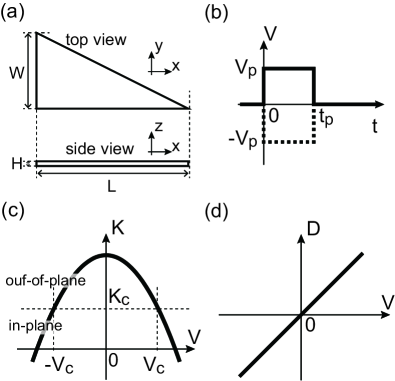
We consider magnetization switching in a perpendicularly magnetized right triangle nanomagnet shown in Fig. 1 (a) by application of a voltage pulse shown in Fig. 1 (b). There are two magnetic states at equilibrium: one is up-polarized state and the other is down-polarized state. Both the MA constant () and the DMI constant () are assumed to be voltage-controllable. Voltage dependence of has been studied by several groupsNozaki et al. (2010); Amiri et al. (2015); Kanai et al. (2014); Lin et al. (2014). Some reported linear voltage dependence Nozaki et al. (2010); Amiri et al. (2015) and others reported non-linear voltage dependence Kanai et al. (2014); Lin et al. (2014). In this study is assumed to be a symmetric function of the voltage () and decreases with increase or decrease of as shown in Fig. 1 (c). There is a critical value, , below which most magnetic moments are aligned in the plane. Since is assumed be a symmetric function of the almost in-plane magnetic state is realized by application of the voltage of , where is the critical voltage.
It should be noted that the demagnetization field at the corners is much weaker than that in the middle. Even at the magnetic moments at the corners have a considerable out-of-plane component. One can modify the direction of the magnetic moments at the corners via the voltage-control of . The DMI is the non-collinear exchange interaction and rotates the magnetic moments. The magnitude of represents the period of rotation. The sign of represents the direction of rotation; i.e., clockwise or anti-clockwise. is assumed to be an anti-symmetric function of as shown in Fig. 1 (d). The direction of rotation of magnetic moments and therefore the direction of magnetic moments at the corners can be controlled by the sign of . Although a material having both the symmetric -dependent and anti-symmetric -dependent has not been fabricated yet, it is important to study the mechanism and conditions for the deterministic switching based on micromagnetic simulations prior to the experiments.
After turning off the voltage the magnetic moments relax to the up-polarized or down-polarized state depending on the magnetic configuration at the corners. In the relaxation process the corners act as nucleation sites. The switching mode is not the coherent rotation but the domain wall displacement. To push the domain wall out of the magnetic element smoothly the magnetic element should have low symmetry shape like a right triangle shown in Fig. 1 (a).
The micromagnetic simulations were performed by using the software package MuMax3Vansteenkiste et al. (2014). We solve the Landau-Lifshitz equation defined as
| (1) |
where is the magnetization unit vector, is time, is the gyromagnetic ratio and is the Gilbert damping constant. The effective field
| (2) |
comprises the external field , the demagnetizing field , the exchange field and the anisotropy field . The external field is applied in the positive -direction: , where , represents the unit vector in the direction of the positive -axis. The definition of the Cartesian coordinates is given in Fig. 1 (a). The anisotropy field is given by
| (3) |
where is the saturation magnetization and is the height of the triangle element shown in Fig. 1 (a). The exchange field comprises the Heisenberg exchange interaction term and the DMI term as
| (4) |
where is the exchange stiffness constant for the Heisenberg interaction.
The width, length and height of the triangle element are assumed to be = 32 nm, = 64nm and = 2 nm, respectively. The system is divided into cubic cells of side length 2 nm. The following material parameters are assumed: saturation magnetization = 1.35 MA/m, exchange stiffness constant = 10 pJ/m. The Gilbert damping constant ranges from 0.1 to 1. The MA constant during the pulse () ranges from 0 to 2 mJ/m2. The MA constant at = 0 is assumed to be 4 mJ/m2. The DMI constant during the pulse () ranges from 0.01 to 2 mJ/m. The DMI constant at = 0 is assumed to be 0. The shape of the voltage pulse is shown in Fig. 1 (b), where and are the amplitude and the duration of the pulse.
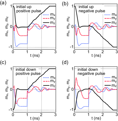
Figures 2 (a)-(d) show the typical examples of the magnetization dynamics. The value of is assumed to be 1 to suppress the precessional motion during the pulse. The -, - and -components of the space averaged magnetization unit vector are plotted by the blue dotted, red dashed and black solid curves, respectively. The external magnetic field of =10 mT is applied in the positive -direction. The initial state is the up-polarized state for Figs. 2 (a) and (b), and is the down-polarized state for Figs. 2 (c) and (d), respectively. The anisotropy constant during the pulse is assumed to be = 1.4 mJ/m2. The DMI constant during the pulse is assumed to be =0.5 mJ/m ( = -0.5 mJ/m ) for the positive (negative) voltage pulse.
In all panels is almost zero at the end of the pulse ( = 1 ns) which means that the almost in-plane polarized magnetic state is realized. After turning off the voltage increases or decreases with increase of depending on the sign of the voltage. For the up-polarized initial state (=1) the magnetization is not switched by the positive voltage pulse but is switched to the down-polarized state (=-1) by the negative voltage pulse as shown in Figs. 2 (a) and (b). For the down-polarized initial state (=-1) the magnetization is not switched by the negative voltage pulse but is switched to the up-polarized state (=1) by the positive voltage pulse as shown in Figs. 2 (c) and (d). These results clearly show that the magnetization direction of the final state is determined by the polarity of the voltage pulse irrespective of the initial state.
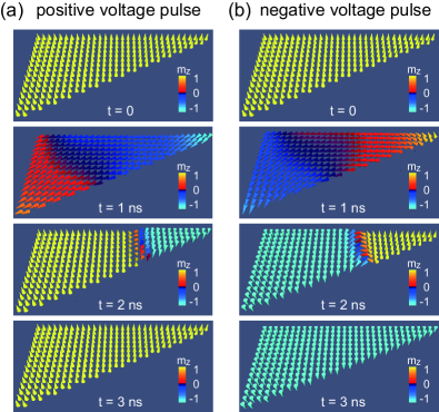
Figures 3 (a) and (b) show the snapshots of the magnetization vectors at =0, 1, 2, 3 ns for the up-polarized initial state. The sign of the voltage pulse is positive for Fig. 3 (a) and negative for Fig. 3 (b). The red-tone represents the positive while the blue-tone represents the negative . The magnetization configuration at the end of the pulse ( = 1 ns) is quite different between the positive and negative voltage pulses. For the positive voltage pulse at the bottom left corner is positive and that at the top right corner is negative as shown in the second panel of Fig. 3 (a). For the negative voltage pulse at the bottom left corner is negative and at the top right corner is positive as shown in the second panel of Fig. 3 (b).
For the positive voltage pulse up-polarized initial state does not switch to the down-polarized sate but returns to the up-polarized state. Once the voltage is turned off the magnetic moments around the bottom left corner tilt upwards to form an up-polarized domain, and those around the top right corner tilt downwards to form a down-polarized domain as shown in the third panel of Fig. 3 (a). Between the up-polarized and down-polarized domains there appears a narrow domain wall which moves to the top right corner to reduce the dmain wall energy. Finally the domain wall is swept out from the magnet, and the up-polarized state is recovered within 3 ns.
Application of the negative voltage pulse switches the magnetization from up-polarized state to the down-polarized state as shown in Fig. 3 (b). After turning off the voltage pulse the magnetic moments around the bottom left corner tilt downwards to form a down-polarized domain, and those around the top right corner tilt upwards to form an up-polarized domain as shown in the third panel of Fig. 3 (b). The domain wall between these two domains moves to the top right corner, and the magnetic state is switched to the down-polarized state within 3 ns.
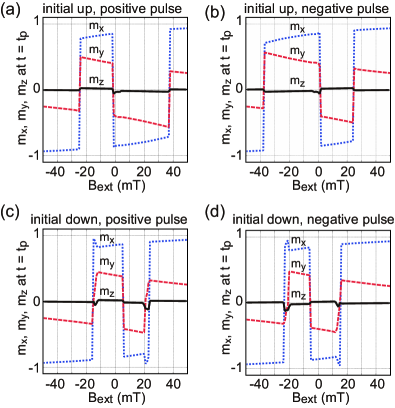
As shown in the second panels of Figs. 3 (a) and 3 (b) the most magnetizaion vectors at the end of the pulse point to the negative -direction in spite that of 10 mT is applied in the positive -direction, which implies that 10 mT is not large enough to align the magnetization vectors along . Figures 4 (a) – 4 (d) show the -dependence of , and at the end of the pulse. The parameters other than are the same as those in Figs. 2 and 3. The magnetization configuration and therefore the values of , and suddenly change at certain values of . At large ( 40 mT) has the same sign as ; i.e. the most magnetization vectors are aligned long the external magnetic field. Comparing Fig. 4 (a) with 4 (b), or 4 (c) with 4 (d), we note that the magnetization configuration at the end of the pulse has the symmetry with respect to the following transformation: . Assuming that the magnetic moments are placed on a two-dimensional plane one can easily show that the LLG equation has the same symmetry.
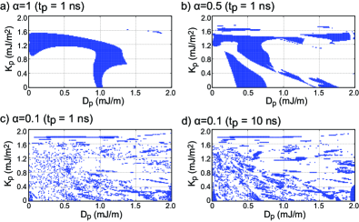
Let us discuss the parameter range where deterministic switching is available. Figure 5 (a) summarizes the simulation results for various values of and with = 1. The simulations are performed in the range of 0.01 mJ/m 2 mJ/m and 0 2 mJ/m2. The pulse width is = 1 ns and the external magnetic field of =10 mT is applied in the positive -direction. The parameters where the deterministic switching is available are plotted by the blue rectangles most of which bunch around the lines with mJ/m2 and mJ/m. The deterministic switching fails for large ( mJ/) because the magnetic moments remains almost perpendicular to the plane at the end of the pulse. At around mJ/m2 the uniaxial anisotropy field is almost canceled by the demagnetization field. Therefore most magnetic moments are aligned in the plane, and the nucleation core at the corners can easily be created by the small value of . For small ( mJ/) the switching region is limited at around 1 mJ/m. As it will be shown later this switching region can be spread down to the lower values of by introducing rise and fall time to the square wave pulse.
Figures 5 (b) and (c) are the same plot for = 0.5 and 0.1, respectively. For the switching region splits into several small pieces and scattered as shown in Fig. 5 (b). Also there appear some switching regions at large ( mJ/). Further decrease of down to 0.1 scatters the switching region into very fine pieces as shown in Fig. 5 (c). In Fig. 5 (d) we plot the results for and =10 ns which is long enough for magnetization to relax. Comparing Fig. 5 (d) with Fig. 5 (c) some switching regions are clustered but the difference between them is not significant. These results imply that the precessional motion of magnetic moments plays an important role in switching failure; i.e. the magnetic moments do not relax into the equilibrium state but into one of the quasi-equilibrium states.
In order to clarify the effect of the precessional motion on switching we calculate the quasi-adiabatic dynamics of magnetic moments. As shown in Fig. 6 (a) the absolute value of the voltage pulse is discretized with 100 points; i.e. we take 100 steps to turn on the voltage and another 100 steps to turn off the voltage. At each voltage the micromagnetic simulation is performed until the magnetic moments are relaxed. Figure 6 (b) is the switching diagram based on the quasi-adiabatic simulations with . Comparing Fig. 6 (b) with Fig. 5 (a) one can clearly see that the failure of switching for mJ/m2 is due to the precessional motion.
Because we assumed the square shape for the voltage pulse the effective field suddenly changes, and the large precessional torque is exerted on the magnetic moments, at the beginning and end of the pulse. The results shown in Figs. 6 (a) and (b) suggest that introduction of rise and fall time to the pulse will spread the switching region in Fig. 5 (a).
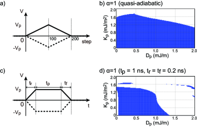
We performed the simulations under the voltage pulse with rise and fall time shown in Fig. 6 (c). The duration of the pulse is assumed to be = 1 ns, and the rise time and the fall time are assumed to be = = 0.2 ns. The other parameters are the same as in Fig. 5 (a). The switching diagram is shown in Fig. 6 (d). Introduction of the rise and fall time of 0.2 ns spreads the switching region; i.e. most of the unswitching region in the bottom left part of Fig. 5 (a) becomes the switching region in Fig. 6 (d).
| 0 | 1 | 2 | 3 | 4 | 5 | 6 | 7 | 8 | 9 | 10 | |
| 0.01 | |||||||||||
| 0.02 | |||||||||||
| 0.05 | |||||||||||
| 0.1 | |||||||||||
| 0.2 | |||||||||||
| 0.5 |
Table 1 summarizes the results for various values of and . The anisotropy constant during the pulse is assumed to be =1.4 mJ/m2. The other parameters are the same as in Fig. 6 (d). Note that the deterministic switching fails for small values of . At the LLG equation is invariant under the transformation of . Because of this symmetry the dynamics of the -component of the magnetic moments and therefore the magnetic state after the voltage pulse are the same for both the positive and the negative voltage pulses. Application of the external field is necessary to break the symmetry of the LLG equation and make the dynamics of different between the positive and the negative voltage pulses.
In summary, based on the micromagnetic simulations it is demonstrated that the voltage-induced changes of MA and DMI can switch the magnetization of a right triangle magnet under in-plane magnetic field. The magnetic state after application of the voltage pulse is determined by the polarity of the voltage irrespective of the initial magnetic state. The mechanism of switching and the conditions for the shape of the magnetic element and material parameters are clarified. The proposed deterministic switching provides the fast and low-power writing method for VC-MRAMs without preread.
This work was partially supported by ImPACT Program of the Council for Science, Technology and Innovation (Cabinet Office, Government of Japan).
References
- Weisheit et al. (2007) M. Weisheit, S. Fahler, A. Marty, Y. Souche, C. Poinsignon, and D. Givord, “Electric Field-Induced Modification of Magnetism in Thin-Film Ferromagnets,” Science 315, 349 (2007).
- Maruyama et al. (2009) T. Maruyama, Y. Shiota, T. Nozaki, K. Ohta, N. Toda, M. Mizuguchi, A. A. Tulapurkar, T. Shinjo, M. Shiraishi, S. Mizukami, Y. Ando, and Y. Suzuki, “Large voltage-induced magnetic anisotropy change in a few atomic layers of iron,” Nature Nanotechnology 4, 158 (2009).
- Nozaki et al. (2010) T. Nozaki, Y. Shiota, M. Shiraishi, T. Shinjo, and Y. Suzuki, “Voltage-induced perpendicular magnetic anisotropy change in magnetic tunnel junctions,” Applied Physics Letters 96, 3 (2010).
- Shiota et al. (2011) Yoichi Shiota, Takayuki Nozaki, Frédéric Bonell, Shinichi Murakami, Teruya Shinjo, and Yoshishige Suzuki, “Induction of coherent magnetization switching in a few atomic layers of FeCo using voltage pulses,” Nature Materials 11, 39 (2011).
- Nozaki et al. (2014) Takayuki Nozaki, Hiroko Arai, Kay Yakushiji, Shingo Tamaru, Hitoshi Kubota, Hiroshi Imamura, Akio Fukushima, and Shinji Yuasa, “Magnetization switching assisted by high-frequency-voltage-induced ferromagnetic resonance,” Applied Physics Express 7, 093005 (2014).
- Lin et al. (2014) Wen Chin Lin, Po Chun Chang, Cheng Jui Tsai, Tsung Chun Shieh, and Fang Yuh Lo, “Voltage-induced reversible changes in the magnetic coercivity of Fe/ZnO heterostructures,” Applied Physics Letters 104, 1 (2014).
- Amiri et al. (2015) Pedram Khalili Amiri, Juan G. Alzate, Xue Qing Cai, Farbod Ebrahimi, Qi Hu, Kin Wong, Cécile Grèzes, Hochul Lee, Guoqiang Yu, Xiang Li, Mustafa Akyol, Qiming Shao, Jordan A. Katine, Jürgen Langer, Berthold Ocker, and Kang L. Wang, “Electric-Field-Controlled Magnetoelectric RAM: Progress, Challenges, and Scaling,” IEEE Transactions on Magnetics 51, 1 (2015).
- Kanai et al. (2016) S. Kanai, F. Matsukura, and H. Ohno, “Electric-field-induced magnetization switching in CoFeB/MgO magnetic tunnel junctions with high junction resistance,” Applied Physics Letters 108, 2014 (2016).
- Grezes et al. (2016) C. Grezes, F. Ebrahimi, J. G. Alzate, X. Cai, J. A. Katine, J. Langer, B. Ocker, P. Khalili Amiri, and K. L. Wang, “Ultra-low switching energy and scaling in electric-field-controlled nanoscale magnetic tunnel junctions with high resistance-area product,” Applied Physics Letters 108, 3 (2016).
- Munira et al. (2016) Kamaram Munira, Sumeet C. Pandey, Witold Kula, and Gurtej S. Sandhu, “Voltage-controlled magnetization switching in MRAMs in conjunction with spin-transfer torque and applied magnetic field,” Journal of Applied Physics 120, 203902 (2016).
- Nozaki et al. (2016) Takayuki Nozaki, Anna Kozioł-Rachwał, Witold Skowroński, Vadym Zayets, Yoichi Shiota, Shingo Tamaru, Hitoshi Kubota, Akio Fukushima, Shinji Yuasa, and Yoshishige Suzuki, “Large Voltage-Induced Changes in the Perpendicular Magnetic Anisotropy of an MgO-Based Tunnel Junction with an Ultrathin Fe Layer,” Physical Review Applied 5, 044006 (2016).
- Shiota et al. (2016) Yoichi Shiota, Takayuki Nozaki, Shingo Tamaru, Kay Yakushiji, Hitoshi Kubota, Akio Fukushima, Shinji Yuasa, and Yoshishige Suzuki, “Evaluation of write error rate for voltage-driven dynamic magnetization switching in magnetic tunnel junctions with perpendicular magnetization,” Applied Physics Express 9, 013001 (2016).
- Nozaki et al. (2017) Takayuki Nozaki, Anna Kozioł-Rachwał, Masahito Tsujikawa, Yoichi Shiota, Xiandong Xu, Tadakatsu Ohkubo, Takuya Tsukahara, Shinji Miwa, Motohiro Suzuki, Shingo Tamaru, Hitoshi Kubota, Akio Fukushima, Kazuhiro Hono, Masafumi Shirai, Yoshishige Suzuki, and Shinji Yuasa, “Highly efficient voltage control of spin and enhanced interfacial perpendicular magnetic anisotropy in iridium-doped Fe/MgO magnetic tunnel junctions,” NPG Asia Materials 9, e451 (2017).
- Dzyaloshinskii (1960) Ie E Dzyaloshinskii, “On the magneto-electrical effect in antiferromagnets,” Journal of Soviet Physics Jetp 10, 628 (1960).
- Moriya (1960) Tôru Moriya, “Anisotropic Superexchange Interaction and Weak Ferromagnetism,” Physical Review 120, 91 (1960).
- Crépieux and Lacroix (1998) A. Crépieux and C. Lacroix, “Dzyaloshinsky-Moriya interactions induced by symmetry breaking at a surface,” Journal of Magnetism and Magnetic Materials 182, 341 (1998).
- Bode et al. (2007) M. Bode, M. Heide, K. von Bergmann, P. Ferriani, S. Heinze, G. Bihlmayer, A. Kubetzka, O. Pietzsch, S. Blügel, and R. Wiesendanger, “Chiral magnetic order at surfaces driven by inversion asymmetry,” Nature 447, 190 (2007).
- Ferriani et al. (2008) P. Ferriani, K. von Bergmann, E. Y. Vedmedenko, S. Heinze, M. Bode, M. Heide, G. Bihlmayer, S. Blügel, and R. Wiesendanger, “Atomic-Scale Spin Spiral with a Unique Rotational Sense: Mn Monolayer on W(001),” Physical Review Letters 101, 027201 (2008).
- Muhlbauer et al. (2009) S. Muhlbauer, B. Binz, F. Jonietz, C Pfleiderer, A Rosch, A Neubauer, Robert Georgii, and P. Boni, “Skyrmion Lattice in a Chiral Magnet,” Science 323, 915 (2009).
- Neubauer et al. (2009) A. Neubauer, C. Pfleiderer, B. Binz, A. Rosch, R. Ritz, P. G. Niklowitz, and P. Böni, “Topological Hall Effect in the A Phase of MnSi,” Physical Review Letters 102, 186602 (2009).
- Pappas et al. (2009) C. Pappas, E. Lelièvre-Berna, P. Falus, P. M. Bentley, E. Moskvin, S. Grigoriev, P. Fouquet, and B. Farago, “Chiral Paramagnetic Skyrmion-like Phase in MnSi,” Physical Review Letters 102, 197202 (2009).
- Thiaville et al. (2012) André Thiaville, Stanislas Rohart, Émilie Jué, Vincent Cros, and Albert Fert, “Dynamics of Dzyaloshinskii domain walls in ultrathin magnetic films,” EPL (Europhysics Letters) 100, 57002 (2012).
- Fert et al. (2013) Albert Fert, Vincent Cros, and João Sampaio, “Skyrmions on the track,” Nature Nanotechnology 8, 152 (2013).
- Ryu et al. (2013) Kwang-Su Ryu, Luc Thomas, See-Hun Yang, and Stuart Parkin, “Chiral spin torque at magnetic domain walls,” Nature Nanotechnology 8, 527 (2013).
- Emori et al. (2013) Satoru Emori, Uwe Bauer, Sung Min Ahn, Eduardo Martinez, and Geoffrey S D Beach, “Current-driven dynamics of chiral ferromagnetic domain walls,” Nature Materials 12, 611 (2013).
- Torrejon et al. (2014) Jacob Torrejon, Junyeon Kim, Jaivardhan Sinha, Seiji Mitani, Masamitsu Hayashi, Michihiko Yamanouchi, and Hideo Ohno, “Interface control of the magnetic chirality in CoFeB/MgO heterostructures with heavy-metal underlayers,” Nature Communications 5, 1 (2014).
- Nawaoka et al. (2015) Kohei Nawaoka, Shinji Miwa, Yoichi Shiota, Norikazu Mizuochi, and Yoshishige Suzuki, “Voltage induction of interfacial Dzyaloshinskii-Moriya interaction in Au/Fe/MgO artificial multilayer,” Applied Physics Express 8, 063004 (2015).
- Han et al. (2016) Dong Soo Han, Nam Hui Kim, June Seo Kim, Yuxiang Yin, Jung Woo Koo, Jaehun Cho, Sukmock Lee, Mathias Kläui, Henk J.M. Swagten, Bert Koopmans, and Chun Yeol You, “Asymmetric hysteresis for probing Dzyaloshinskii-Moriya interaction,” Nano Letters 16, 4438 (2016).
- Skyrme (1962) T.H.R. Skyrme, “A unified field theory of mesons and baryons,” Nuclear Physics 31, 556 (1962).
- Kanai et al. (2014) S. Kanai, Y. Nakatani, M. Yamanouchi, S. Ikeda, H. Sato, F. Matsukura, and H. Ohno, “Magnetization switching in a CoFeB/MgO magnetic tunnel junction by combining spin-transfer torque and electric field-effect,” Applied Physics Letters 104, 9 (2014).
- Vansteenkiste et al. (2014) Arne Vansteenkiste, Jonathan Leliaert, Mykola Dvornik, Mathias Helsen, Felipe Garcia-Sanchez, and Bartel Van Waeyenberge, “The design and verification of MuMax3,” AIP Advances 4, 107133 (2014).