Radiation hardness of a p-channel notch CCD developed for the X-ray CCD camera onboard the XRISM satellite
Abstract
We report the radiation hardness of a p-channel CCD developed for the X-ray CCD camera onboard the XRISM satellite. This CCD has basically the same characteristics as the one used in the previous Hitomi satellite, but newly employs a notch structure of potential for signal charges by increasing the implant concentration in the channel . The new device was exposed up to approximately protons cm-2 at 100 MeV. The charge transfer inefficiency was estimated as a function of proton fluence with an 55Fe source. A device without the notch structure was also examined for comparison. The result shows that the notch device has a significantly higher radiation hardness than those without the notch structure including the device adopted for Hitomi. This proves that the new CCD is radiation tolerant for space applications with a sufficient margin.
1 Introduction
The X-Ray Imaging and Spectroscopy Mission (XRISM), recently renamed from XARM, is the seventh Japanese X-ray astronomical satellite planned to be launched in the early 2020’s [1]. XRISM will carry two identical X-ray mirror assemblies. One of the focal plane detectors is an X-ray microcalorimeter array, which will provide unprecedented high-resolution X-ray spectroscopy with a relatively narrow field of view (FOV) of [2]. The other is an X-ray charge-coupled device (CCD) camera, which has moderate energy resolution with a large FOV of [3]. These two instruments play complementary roles to each other and will open up a new view of the X-ray universe.
The XRISM CCD has basically the same characteristics as the one used in the previous Hitomi satellite [4], a p-channel back-illuminated device with a full-depletion layer with a thickness of 200 m. As is the case with Hitomi, XRISM will fly in the low earth orbit with an altitude of 575 km and an inclination angle of . Devices in this orbit are exposed to a large number of cosmic rays, dominated by geomagnetically trapped protons in the South Atlantic Anomaly, and the average dose rate of protons is estimated to be in the case of the Hiromi CCD [5]. The non-ionizing energy loss of cosmic-ray protons results in bulk damage in silicon. It increases the charge transfer inefficiency (CTI) defined as a fraction of charge loss per one-pixel transfer and degrades the spectroscopic performance of X-ray CCDs in space.
In the case of Hitomi, in order to mitigate the radiation damage effects, we cooled the CCD temperature down to C and employed the charge injection (CI) technique, which reduces signal packet loss by filling traps with regularly spaced injected charges [6, 7]. For further improvement, we newly introduced a “notch” structure to the XRISM CCD. The notch structure is a narrow implant in the CCD channel confining a charge packet to a fraction of the pixel volume in an additional potential well and has been known to reduce the CTI [8, 9].
In this paper, we report the results of radiation damage experiments for studying the radiation hardness of our new notch device, especially paying attention to the application to the XRISM satellite.
2 Experiment
| architecture | frame-transfer |
|---|---|
| channel type | p-channel |
| clock phase | 2 |
| pixel size | |
| pixel format | 320(H) 256(V) |
| imaging area size | 7.7 6.1 mm2 |
| binning | 2 2 |
| frame cycle | 4 s |
| operating temperature |
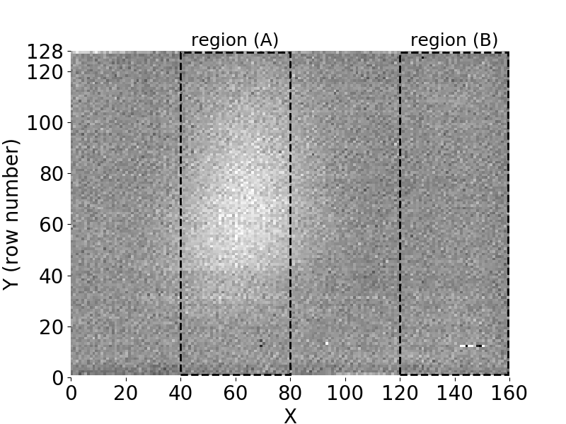
Table 1 shows the specifications and operation parameters of the CCDs under test. The devices are the same as the flight model except for their smaller pixel format [3]. Since the on-chip binning is applied, the frame format obtained is effectively a quarter of the pixel format. In order to evaluate the effect of the notch structure, we fabricated two CCDs. One device has a notch structure, and the other does not. We hereafter call them “notch CCD” and “notchless CCD”.
The radiation damage experiments were performed at HIMAC, which is a synchrotron facility for heavy ion therapy at the National Institute of Radiological Sciences in Japan. The beamline used in the experiment was PH1, which can provide a proton pencil beam with transverse profile approximated by Gaussian-shape with a standard deviation of 1 mm, much smaller than the CCD size of 7 mm. The beam of 100 MeV protons was directly incident on the devices under atmospheric pressure and at room temperature. We repeated the same experiment for the notch and notchless CCDs, and the numbers of incident protons were and , respectively. After the irradiation, CTI was measured with an 55Fe source at in our laboratory. Figure 1 represents the dark current distribution of the notchless CCD after the experiment. The notch CCD also showed a similar profile to the distribution. It is clear that pixels with higher dark current are localized due to the concentration of the proton beam around the center of the imaging area. In the following analysis, we focus on region (A) in and (B) in to represent severely and scarcely damaged areas, respectively (Figure 1).
3 Analysis & Result
|
Region (A)
|
Region (B)
|
||
|
|
|
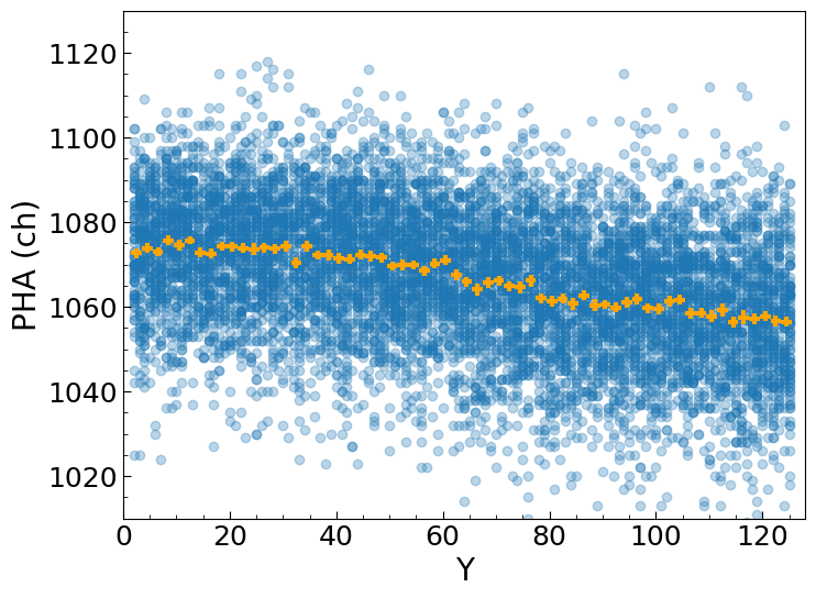
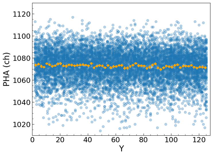
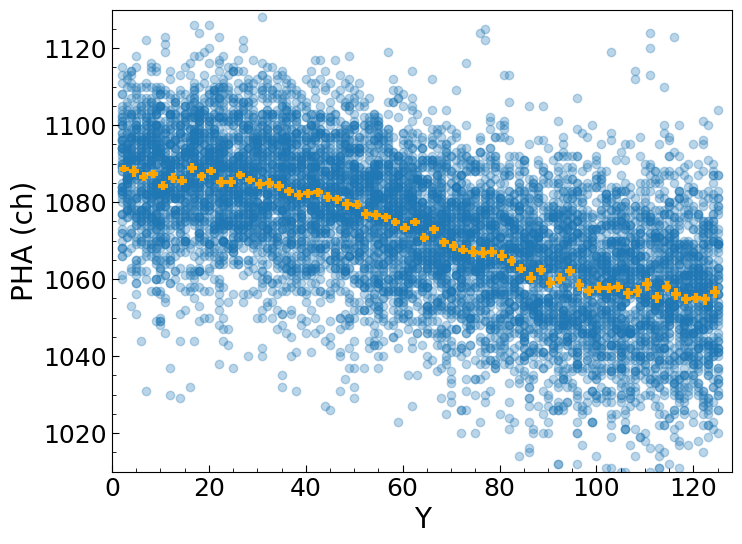
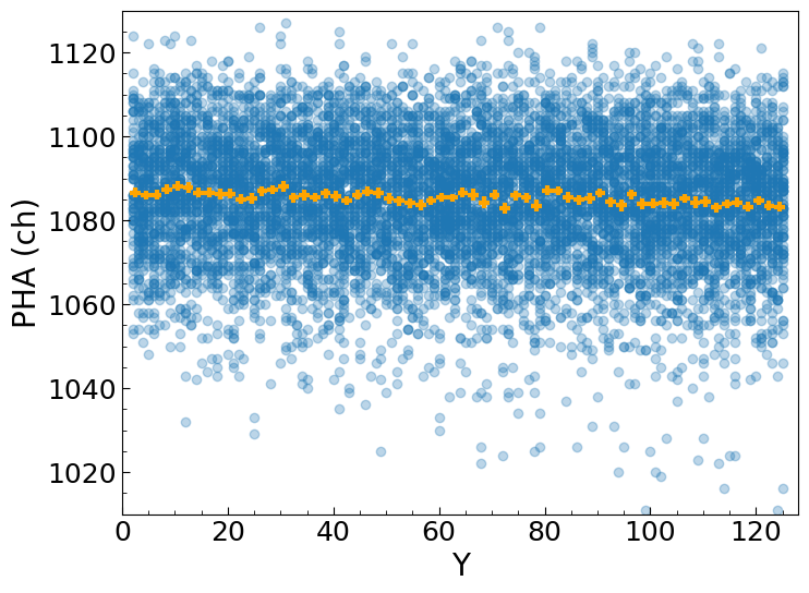
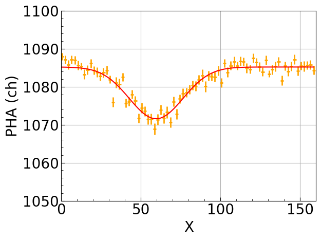
Figure 2 shows the pulse heights of X-ray events produced by the Mn-K line from an 55Fe source as a function of the row number of Y. The Y value corresponds to half the number of transfers because of the binning. The single pixel events in which signal charges are confined in one pixel are used. In region (B), where the proton fluence was almost zero, pulse heights barely reduce with increment in the number of transfers. On the other hand, the events in region (A), where the beam was incident, apparently and non-linearly lost charges as the number of transfers increases. Comparing the notch and notchless CCD results (comparing upper and lower panels), the pulse height reduction of the notch CCD is smaller in spite of the larger total number of the incident protons to the notch CCD. It qualitatively indicates that the CTI degradation of the notch CCD is mitigated by employing the notch structure.
3.1 Measurement of CTI
Defining that is the value of the CTI in the charge transfer between the row numbers of and in the 22 binned format, CTI can be quantitatively evaluated by fitting the pulse heights with the function of the row number as below:
| (3.1) |
where is the row number of a binned pixel at which X-ray is incident, is the pulse height corresponding to the original charge produced by the Mn-K line, and is the pulse height observed at the binned pixel with the row number . If the were constant, the equation (3.1) could be simplified as , which well describes the experimental situation where the radiation damage was uniform across the imaging area [5]. Since the proton fluence differed in each row in this case, the simplified function does not apply. Considering that the beam has a Gaussian-shape profile, we assumed that is represented by the following Gaussian function:
| (3.2) |
where is the maximum CTI, is the center of the beam axis, is the beam width, and is the initial value of the CTI measured before the experiment.
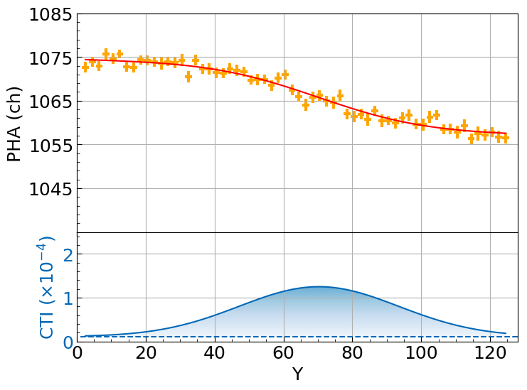
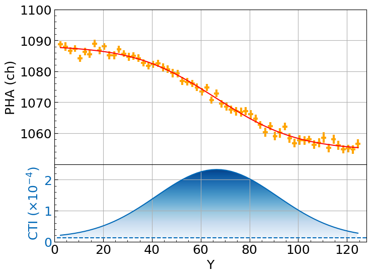
Figure 3 shows the fit results. All datasets are well described by the composite model consisting of the equations (3.1) – (3.2), and the parameters obtained are reasonable. For example, in the notchless CCD case was , which matches the peak of the dark current distribution shown in figure 1 and where the pulse height reduction is the largest. The same applies to the notch CCD case.
3.2 Estimation of the proton fluence in each row
In order to quantify the relation between the CTI and the radiation damage at each row, the proton fluence in each row also needs to be estimated. Since the total number of the incident protons to the imaging area was measured, the proton fluence in the row of was estimated by integration of the beam distribution:
| (3.3) |
where is the proton fluence in the row of , is the total protons incident to the imaging area, and is a normalized beam distribution. We approximated the beam distribution as a 2D Gaussian function. The value of the vertical width was taken from the CTI model fitting described above while that of the horizontal width was estimated by fitting the horizontal profile of pulse heights with the Gaussian function as shown in figure 4.
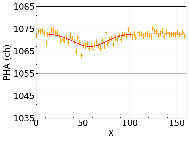
This horizontal profile was made from the single pixel events in the region of 40 Y 80 where the damage was the most severe. The vertical and horizontal widths in the notchless CCD case were mm and mm, respectively. Similar values were obtained in the notch CCD case. These values were consistent with those measured at the beam monitor in the upper stream of our system [10], especially in terms of the ratio of the vertical and horizontal widths. In our estimation, the notch and notchless CCDs were irradiated by up to protons cm-2 and protons cm-2 in the highest fluence area, respectively.
3.3 Evolution of CTI as a function of the equivalent time in orbit
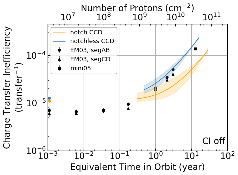
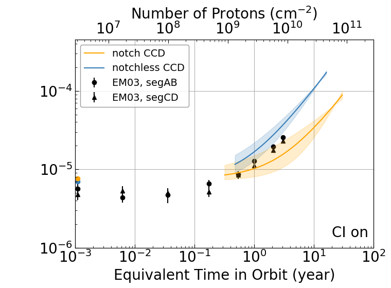
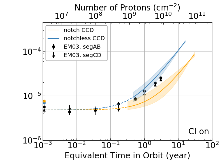
Figure 5 shows the CTI as a function of the equivalent time in the low earth orbit where the XRISM satellite is planned to be injected. This figure basically plots vs obtained above, and is converted to equivalent time in the XRISM orbit following Mori et al. (2013) [5]. It is clear that the introduction of the notch structure mitigates the increase of CTI by a factor of 2–3 (comparison between blue and orange lines). Comparison with our previous measurement of the notchless Hitomi CCD, which was performed with an 55Fe source at C, also shows the effectiveness of the notch structure (comparison between black dots and the orange line). Since we had already shown that even the notchless CCD adopted for Hitomi was radiation tolerant enough for space use [5], these results suggest that our new notch CCD has a sufficient margin of radiation tolerance for the application to XRISM. We also confirmed that the CI technique effectively works for both types of the CCDs (comparison between left and right figures).
4 Discussion
We performed proton radiation damage experiments on our newly developed notch CCD and previously developed notchless CCD, and verified the effectiveness of the notch structure in this simple control experiment. The introduction of the notch structure improved radiation hardness of our device by a factor of 2–3. Other experiments using different manufacturing p-channel CCDs have also reported a similar degree of improvement from comparisons of their notch and notchless devices [8, 11]. We note that experimental conditions, such as proton beam energy and CCD working temperature, are different among experiments including ours. Although the detailed manufacturing processes regarding the notch implant of each device are not available, this might suggest that the width ratios between the notch implant and the channel are similar to each other.
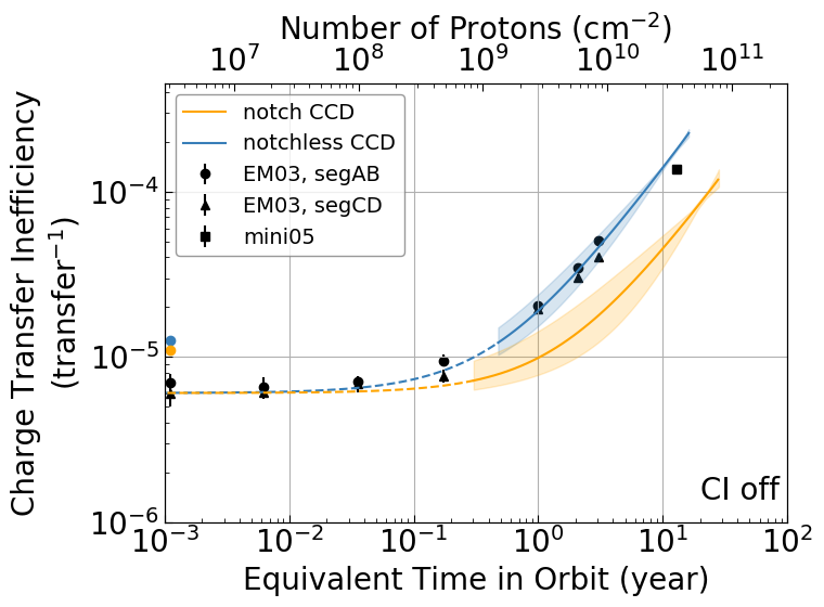
The notchless CCD is basically the same as that adopted for Hitomi and thus it is expected that their radiation hardness is comparable. However, in figure 5, the CTI degradation of the notchless CCD used in this experiment appears to be greater than or equal to that of the Hitomi CCD (comparison between the blue line and black dots). Figure 6 is the same as figure 5 but the initial CTI values of the notch and notchless CCDs used in this experiment are hypothetically set to the same value of the Hitomi CCD. Here, we only changed the initial CTI values and the rest of the parameters in the equations (3.1)–(3.2) are fixed to the best fit values. Although the hypothetical notchless CCD curves are yet to correspond completely to the Hitomi CCD data, the initial CTI value differences may be a part of the reasons for the difference between the notchless CCD and the Hitomi CCDs in figure 5.
Acknowledgments
This work was performed as a part of accelerator experiments of the Research Project at NIRS-HIMAC. We would like to express our thanks to HIMAC crews for their kind support throughout the experiments. This work was also supported by JSPS KAKENHI Grant Number 16H03983 (K.M.), and 15H03641, 18H01256 (H.N.).
References
- [1] M. Tashiro, H. Maejima, K. Toda, R. Kelley, L. Reichenthal, J. Lobell et al., Concept of the X-ray Astronomy Recovery Mission, in Sp. Telesc. Instrum. 2018 Ultrav. to Gamma Ray (J.-W. A. den Herder, K. Nakazawa and S. Nikzad, eds.), vol. 10699 of Society of Photo-Optical Instrumentation Engineers (SPIE) Conference Series, p. 1069922, SPIE, jul, 2018. DOI.
- [2] Y. Ishisaki, R. L. Kelley, H. Akamatsu, H. Awaki, T. G. Bialas, G. V. Brown et al., Status of resolve instrument for x-ray astronomy recovery mission (Conference Presentation), in Sp. Telesc. Instrum. 2018 Ultrav. to Gamma Ray (J.-W. A. den Herder, K. Nakazawa and S. Nikzad, eds.), vol. 10699, p. 2313440, SPIE, jul, 2018. DOI.
- [3] K. Hayashida, H. Tomida, K. Mori, H. Nakajima, T. Tanaka, H. Uchida et al., Soft x-ray imaging telescope (Xtend) onboard X-ray Astronomy Recovery Mission (XARM), in Sp. Telesc. Instrum. 2018 Ultrav. to Gamma Ray (J.-W. A. den Herder, K. Nakazawa and S. Nikzad, eds.), vol. 10699 of Society of Photo-Optical Instrumentation Engineers (SPIE) Conference Series, p. 1069923, SPIE, jul, 2018. DOI.
- [4] T. Takahashi, M. Kokubun, K. Mitsuda, R. L. Kelley, T. Ohashi, F. Aharonian et al., Hitomi (ASTRO-H) X-ray Astronomy Satellite, J. Astron. Telesc. Instruments, Syst. 4 (mar, 2018) 021402.
- [5] K. Mori, Y. Nishioka, S. Ohura, Y. Koura, M. Yamauchi, H. Nakajima et al., Proton radiation damage experiment on P-Channel CCD for an X-ray CCD camera onboard the ASTRO-H satellite, Nucl. Instruments Methods Phys. Res. Sect. A Accel. Spectrometers, Detect. Assoc. Equip. 731 (dec, 2013) 160–165.
- [6] H. Nakajima, Y. Maeda, H. Uchida, T. Tanaka, H. Tsunemi, K. Hayashida et al., In-orbit performance of the soft X-ray imaging system aboard Hitomi (ASTRO-H), Publ. Astron. Soc. Japan 70 (mar, 2018) 21.
- [7] T. Tanaka, H. Uchida, H. Nakajima, H. Tsunemi, K. Hayashida, T. G. Tsuru et al., Soft X-ray Imager aboard Hitomi (ASTRO-H), J. Astron. Telesc. Instruments, Syst. 4 (jan, 2018) 0011211.
- [8] C. Bebek, D. Groom, S. Holland, A. Karcher, W. Kolbe, J. Lee et al., Proton radiation damage in p-channel CCDs fabricated on high-resistivity silicon, IEEE Trans. Nucl. Sci. 49 (2002) 1221–1225.
- [9] H. Tsunemi, M. Miki, E. Miyata, J. Hiraga and K. Miyaguchi, CTI distribution within a damaged CCD pixel having a notch structure, in Hard X-Ray Gamma-Ray Detect. Phys. V (L. A. Franks, A. Burger, R. B. James and P. L. Hink, eds.), vol. 5198, pp. 111–118, SPIE, jan, 2004. DOI.
- [10] M. Torikoshi, K. Noda, E. Takada, T. Kanai, S. Yamada, H. Ogawa et al., Beam monitor system for high-energy beam transportation at HIMAC, Nucl. Instruments Methods Phys. Res. Sect. A Accel. Spectrometers, Detect. Assoc. Equip. 435 (1999) 326–338.
- [11] C. J. Marshall, P. W. Marshall, A. Wacynski, E. Polidan, S. D. Johnson and A. Campbell, Comparisons of the proton-induced dark current and charge transfer efficiency responses of n- and p-channel CCDs, in Proceedings of the SPIE (J. D. Garnett and J. W. Beletic, eds.), vol. 5499, pp. 542–552, sep, 2004. DOI.