Evidence of charge density wave with anisotropic gap in monolayer VTe2 film
Abstract
We report experimental evidence of charge density wave (CDW) transition in monolayer 1T-VTe2 film. 44 reconstruction peaks are observed by low energy electron diffraction below the transition temperature = 186 K. Angle-resolved photoemission spectroscopy measurements reveal arc-like pockets with anisotropic CDW gaps up to 50 meV. The anisotropic CDW gap is attributed to the imperfect nesting of the CDW wave vector, and first-principles calculations reveal phonon softening at the same vector, suggesting the important roles of Fermi surface nesting and electron-phonon interaction in the CDW mechanism.
In layered transition-metal dichalcogenides (TMDCs) Wang et al. (2012); Chhowalla et al. (2013); Manzeli et al. (2017), the electronic structure strongly depends on the sample thickness and quantum confinement effect can result in novel electronic properties and correlated phenomena, e.g. charge density wave (CDW) Castro Neto (2001); Wilson et al. (1975); Grüner (1988), which are distinctive from the bulk materials. Vanadium dichalcogenide films have attracted intensive attention due to their intriguing properties, e.g., 2D magnetism and CDW. Although bulk VSe2 crystal is paramagnetic van Bruggen and Haas (1976); Bayard and Sienko (1976), room temperature ferromagnetism has been recently reported in monolayer VSe2 film Bonilla et al. (2018); Liu et al. (2018). Moreover, atomically thin VSe2 films also exhibit rich CDW orders. While bulk VSe2 crystal shows 43 CDW transition at 110 K Strocov et al. (2012), various CDW orders with different periods and transition temperatures have been reported for monolayer VSe2 film, e.g., 44 CDW order below 140 K Feng et al. (2018); Umemoto et al. (2019), CDW below 220 K Chen et al. (2018), and 2 CDW orders with transition temperatures of 135 K and 350 K, respectively Duvjir et al. (2018).
Compared to VSe2, another vanadium dichalcogenide - VTe2, is much less explored. Bulk VTe2 shows more complicated phases with a structural phase transition from the high temperature 1T phase to the low temperature 1T′ phase at 482 K, and CDW order of 33 has been suggested in the 1T′ phase Bronsema et al. (1984); Nakamura et al. (2018). Few-layer VTe2 films, however, show 1T structure similar to VSe2. Ferromagnetism has been reported in nanoplates of 1T-VTe2 Li et al. (2018), and two possible CDW transitions at 240 K and 135 K have been reported in films of approximately ten layers thick from resistivity measurements Ma et al. (2019). However, the corresponding periods of those CDW orders remain unknown. Moreover, so far there is no report on the growth of monolayer VTe2 film or its electronic structure. Resolving the CDW order in monolayer VTe2 film and revealing the underlying mechanism are important.
Here we report the electronic structure of monolayer VTe2 film grown by molecular beam epitaxy (MBE). Evidence of 44 CDW ordering is reported in the low energy electron diffraction (LEED) below CDW transition temperature = 186 K. Angle-resolved photoemission spectroscopy (ARPES) measurements further reveal anisotropic CDW gaps arising from the V 3d orbital, forming arc-like Fermi surface. The anisotropic gaps can be explained by the imperfect nesting of the hole pockets. First-principles calculations of the phonon spectrum reveal phonon softening at the corresponding CDW wave vector, suggesting the important roles of electron-phonon interaction and Fermi surface nesting in the CDW mechanism.

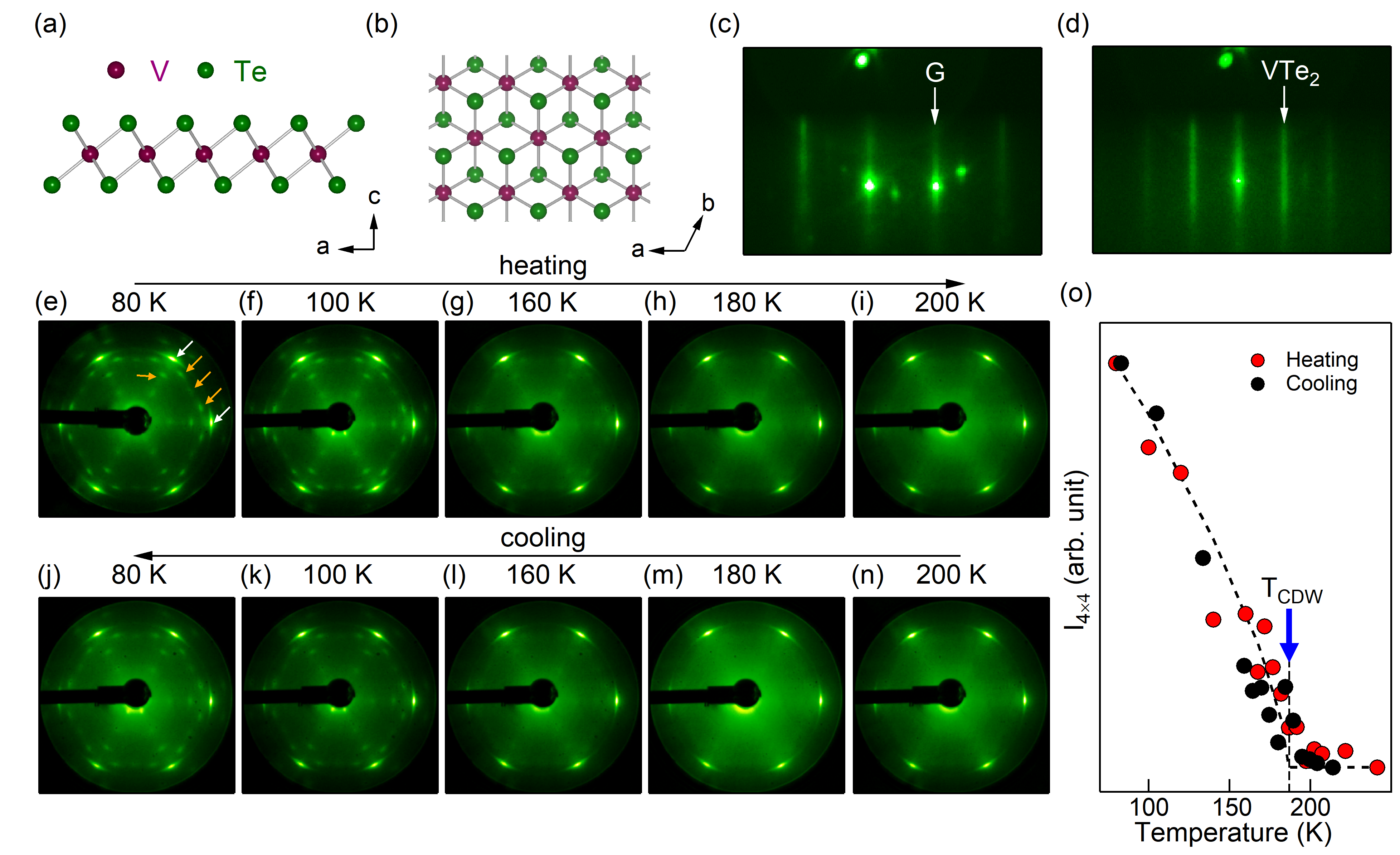
Monolayer 1T-VTe2 consists of one layer of V atoms sandwiched between two layers of Te with space group 1 (Figs. 1(a) and (b) for the side and top views). Monolayer 1T-VTe2 film is grown on bilayer graphene (BLG)/SiC(0001) substrate Wang et al. (2013) by MBE. The growth process is monitored by in situ reflection high-energy electron diffraction (RHEED). Sharp patterns from the graphene substrate [Fig. 1(c)] and 1T-VTe2 film [Fig. 1(d)] are observed in the RHEED patterns before and after growth of 1T-VTe2 film. Using the lattice constant of graphene as a reference, the lattice constant of VTe2 is extracted to be a = 3.63 Å, which is similar to that of the nanoplate 3.64 Å Li et al. (2018) and previous thicker MBE films 3.67 Å Ma et al. (2019). As shown in Fig. S1 and Table SI in the Supplemental Material Sup , there is no significant change on lattice constant for 1T-VTe2 film on BLG within a large growth temperature range, confirming the weak van der Waals interaction between the film and the substrate.
Figure 1(e) shows LEED pattern of monolayer VTe2 film measured at 80 K. In addition to the Bragg spots from VTe2 (pointed by white arrows), additional diffraction spots (pointed by yellow arrows) with 44 period are observed, suggesting the CDW order of 44. Figures 1(e)-1(i) show the evolution of the LEED patterns with increasing temperature. The intensity of 44 diffraction spots decreases with temperature and fully disappears around 180 K, suggesting that the CDW transition occurs near this temperature. When cooling down below 180 K [Figs. 1(n)-(j)], the 44 diffraction peaks are observed again, confirming that the 44 reconstruction is an intrinsic temperature effect associated with the CDW transition. To quantify the CDW transition temperature, we show in Fig. 1(o) the normalized intensity of 44 peak as a function of temperature. By tracking the temperature-dependent LEED measurements, we determine the CDW transition temperature to be 186 K. Similar CDW with weaker 44 period has been reported in monolayer VSe2 film below =140 K Feng et al. (2018).

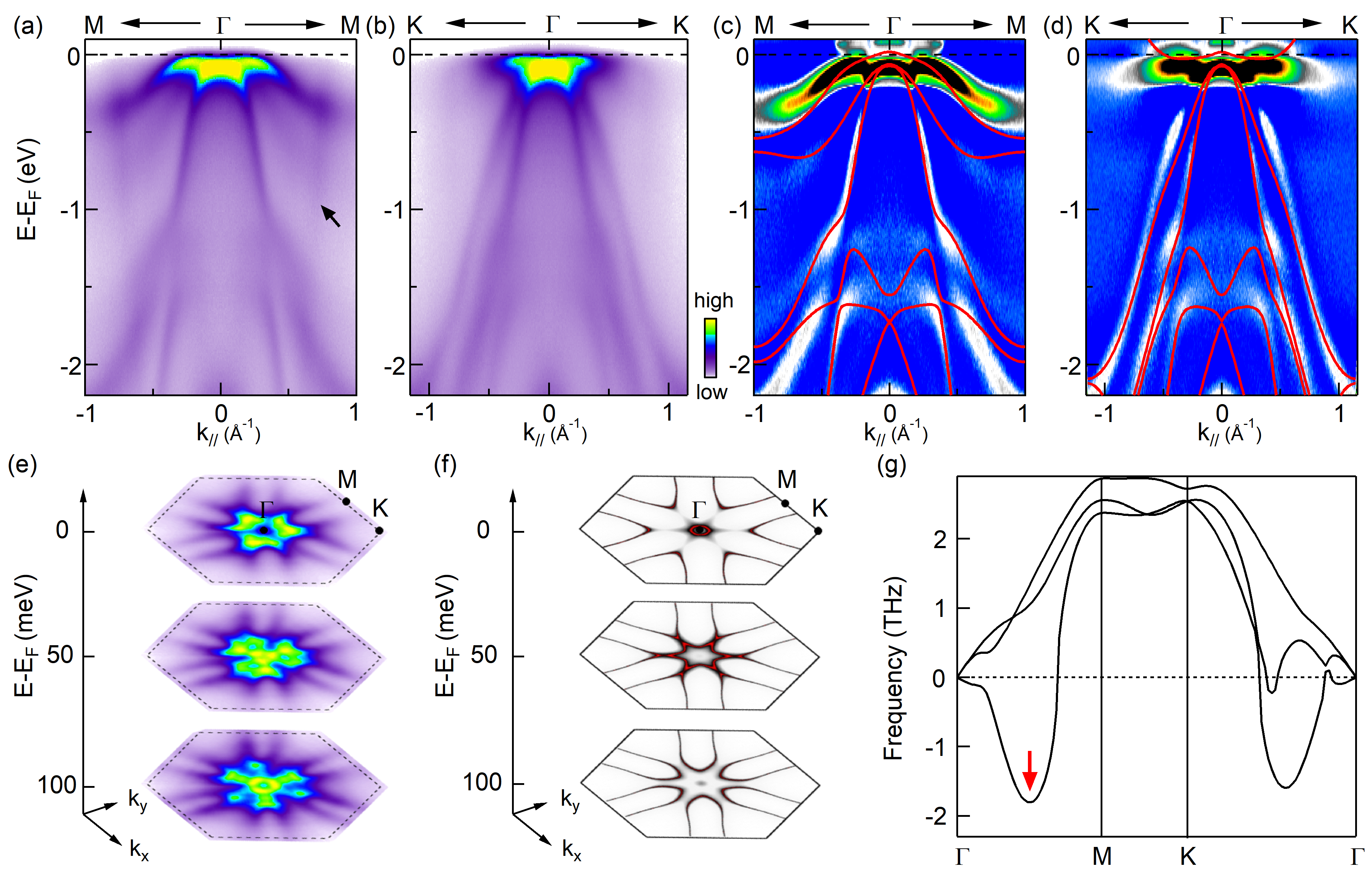
ARPES measurements have been performed to further reveal the electronic structure and the CDW gap. Figures 2(a) and 2(b) show the dispersions measured along two high symmetry directions -M and -K, respectively. Near the point, there is a rather flat band near the Fermi energy () from the V 3d orbital and a hole pocket from Te 4p orbital that extends to -2 eV (See Fig. S2 in the Supplemental Material Sup ). These two pockets touch at -0.03 eV. Near the M point, there is an electron pocket with the bottom of the band at -0.4 eV. In addition, there are folded bands (pointed by black arrow) which are translated by the high energy Te 4p hole pocket at the point by a wave vector = 1/2 a∗ (a∗ is the reciprocal lattice vector), suggesting that in addition to the 44 reconstruction, there is 22 superstructure. Similar 22 order has also been observed in other CDW systems, e.g., TiSe2 Chen et al. (2015). Figures 2(c) and 2(d) show the corresponding second derivative of dispersion images along -M and -K and the calculated band dispersion (red curve) by VASP for non-magnetic monolayer VTe2. There is an overall agreement between the calculated and experimental band dispersions, suggesting that the 1ML VTe2 film is nonmagnetic. The band structure of monolayer VTe2 is similar to monolayer VSe2 and in sharp contrast with bulk VSe2 and VS2 . For bulk VSe2, the Fermi surface contour consists of six elliptical pockets at the M points and gaps only open at the flat portions Strocov et al. (2012). For VS2, the Fermi surface nesting is absent in CDW state, where electron-phonon coupling becomes the dominant driving force Mulazzi et al. (2010).
Figures 2(e)-2(f) show a comparison of the ARPES intensity maps at 0, -50 and -100 meV relative to and the calculated intensity maps. The Fermi surface map shows a circular pocket at the point surrounded by six triangular pockets centered at the K points. Below the Fermi energy, the pockets around the K points start to merge with the expanded pocket at the point, and they evolve into elliptical hole pockets around the M points. The calculated intensity maps [Fig. 2(f)] are in good agreement with the experimental intensity maps [Fig. 2(e)]. In addition, at , the intensity of the triangular pockets decreases quickly when moving away from the point, suggesting possible CDW gap opening near the M point. The calculated phonon spectrum [Fig. 2(g)] clearly indicates that VTe2 is indeed dynamically unstable. The most unstable phonon mode is around the mid-point in the -M path (indicated by the red arrow), which is consistent with 44 CDW order observed in the monolayer film. This suggests that electron-phonon interaction plays an important role in the 44 CDW order formation.

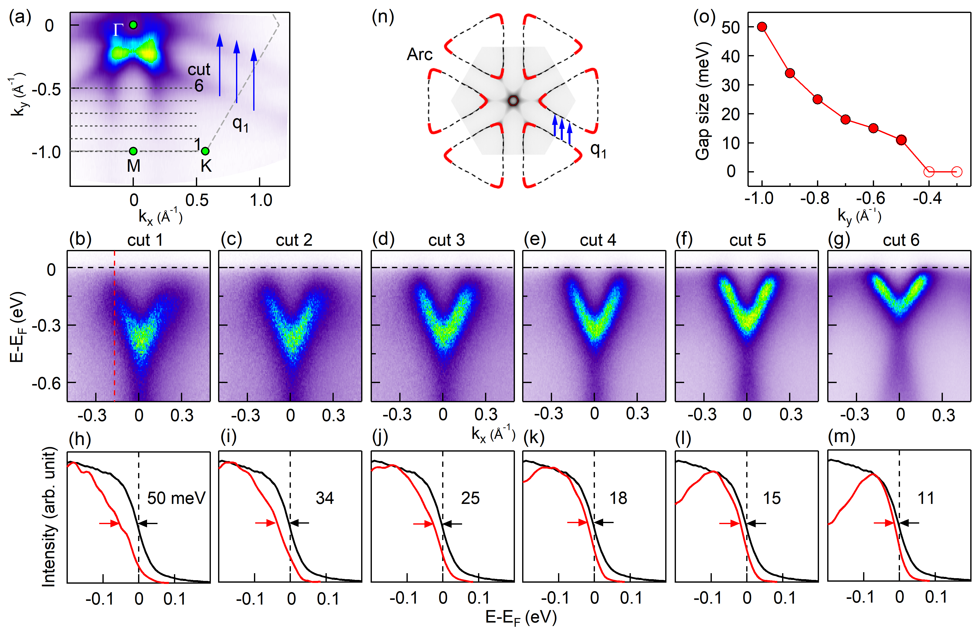
To extract the CDW gap, we show a systematic analysis of the electronic structure near in Fig. 3. Figure 3(a) shows the Fermi surface map. The 44 wave vector connects well the straight parts of the triangular pockets centered at the K points, indicating Fermi surface nesting. Figures 3(b)-3(g) show the dispersions measured at a few cuts parallel to the M-K direction indicated by black dashed lines Fig. 3(a). Near the M point (cut 1), there is a strong suppression of intensity near , indicating that there is a gap opening. Moving toward the point from cut 1 to cut 6, the suppression of intensity moves toward , indicating decreasing of the gap size. To quantify the gap size, we show in Figs. 3(h)-3(m) a comparison of the energy distribution curves (EDCs) at the Fermi momentum (red curve) and the Fermi energy reference (black). The CDW gap is extracted from the shift of the EDC leading edge compared to that in the Fermi energy reference and plotted in Fig. 3(o). Here the largest gap size is 50 meV along the M-K direction, and it decreases to 11 meV for cut 6 and eventually vanishes near the point (see Fig. S3 in the Supplemental Material Sup ), forming arc-like Fermi surface. The anisotropic CDW gap is attributed to the imperfect nesting. As schematically shown in Fig. 3(n), the wave vector connects the two parallel parts of the triangular pockets and the gap is the maximum here. Moving toward the point, the nesting becomes worse due to the rounded shape near the apex of the triangular pocket, resulting in a reduced gap size. We note that anisotropic CDW gap induced by imperfect nesting is also observed in SmTe3 Gweon et al. (1998), CeTe3 Brouet et al. (2004) and NbSe2 Borisenko et al. (2009). The energy and momentum resolved capability of ARPES measurements allows us to resolve arc-like Fermi surface and the anisotropic gap due to imperfect nesting of the Fermi surface. Such anisotropic gap is different from that reported in VSe2 where the entire Fermi surface (including the triangular pockets centered at the K points and the circular pockets at the point) is gapped Feng et al. (2018), suggesting that their CDW mechanisms are different, despite the apparently similar CDW order of 44.

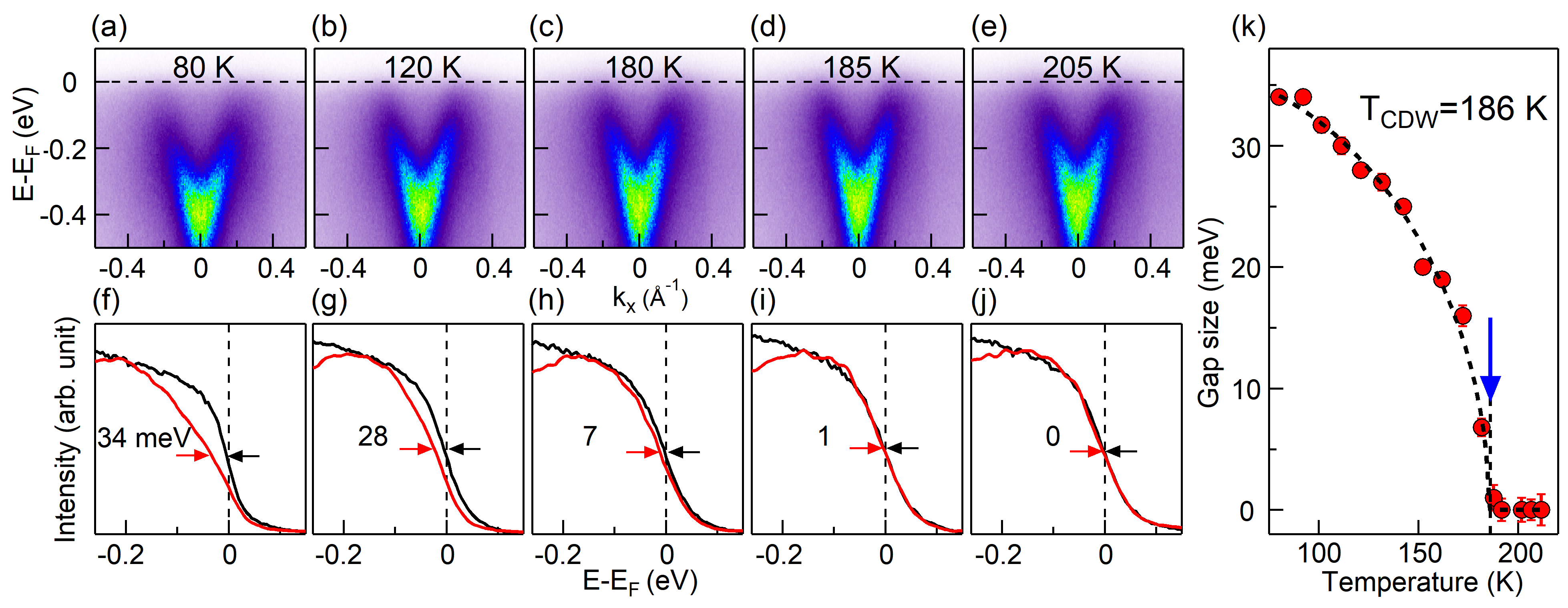
Figure 4 shows the evolution of the gap size with temperature. With increasing temperature, the top of the valance band moves gradually to at higher temperature [Figs. 4(a)-(e)], indicating the decrease of the gap size with temperature. The corresponding EDCs are shown as red curves in Figs. 4(f)-4(j), and the extracted gap size as a function of temperature is shown in Fig. 4(k). The gap size is fitted with mean-field theory Chen et al. (2015); Zhang et al. (2018)
| (1) |
where A is a fitting constant. By fitting the gap size, the CDW transition temperature is extracted to be = 186 5 K, consistent with the LEED measurements. Taking the maximum gap value of 50 meV and = 186 K, the value of coupling ratio is 2 = 6.23. We note that the value of coupling ratio varies in different TMDCs systems, e.g., 6.4 and 17.85 for TaSe2 monolayer Borisenko et al. (2008); Ryu et al. (2018). The extracted ratio for VTe2 film is larger than 3.52 expected for weak-coupled systems, and smaller than the recently reported values of 10 and 38 on monolayer VSe2 Feng et al. (2018); Umemoto et al. (2019).
We would like to further discuss the driving mechanism of CDW order in monolayer 1T-VTe2 film, and its comparison to CDWs reported in bulk VTe2 as well as VSe2 films. The observation of 44 CDW in 1T-VTe2 monolayer film is different from 1T′-VTe2 bulk crystal which holds a double zigzag chain-like 33 CDW pattern Bronsema et al. (1984). Few-layer 1T-VTe2 films on mica have suggested two possible CDW transitions Ma et al. (2019), yet the CDW wave vector and gap size still await to be measured. Compared to previous VSe2 film with reported 44 CDW order Feng et al. (2018), the observation of anisotropic gap opening in our work instead of fully gapped Fermi surface suggests that Fermi surface nesting plays a more important role in the CDW formation of our 1T-VTe2 film. Our ARPES measurements together with phonon spectrum show that both Fermi surface nesting and electron-phonon interaction are the driving forces of CDW formation in monolayer VTe2 films. Similar CDW mechanisms have also been discussed in monolayer 1T-VSe2 film yet with a very different CDW vector Chen et al. (2018), suggesting that there are multiple phonon instabilities in the vanadium dichalcogenide films. The difference can be attributed to substrate, film thickness or stoichiometry. Further investigation is important to obtain a complete understanding of the evolution of rich CDW physics in vanadium dichalcogenide with thickness and substrates.
In summary, we report the 44 CDW order in monolayer 1T-VTe2 film with = 186 K. The observation of anisotropic CDW gap and phonon instability in the calculated phonon spectrum suggest that both Fermi surface nesting and phonon instability contribute significantly to the CDW formation.
This work is supported by the National Natural Science Foundation of China (Grants No. 11725418 and No. 11674188), Ministry of Science and Technology of China (Grants No. 2016YFA0301004, No. 2016YFA0301001, and No. 2015CB921001), Science Challenge Project (No. TZ2016004) and Beijing Advanced Innovation Center for Future Chip (ICFC).
References
- Wang et al. (2012) Q. H. Wang, K. Kalantar-Zadeh, A. Kis, J. N. Coleman, and M. S. Strano, Electronics and optoelectronics of two-dimensional transition metal dichalcogenides, Nat. Nanotechnol. 7, 699 (2012).
- Chhowalla et al. (2013) M. Chhowalla, H. S. Shin, G. Eda, L.-J. Li, K. P. Loh, and H. Zhang, The chemistry of two-dimensional layered transition metal dichalcogenide nanosheets, Nat. Chem. 5, 263 (2013).
- Manzeli et al. (2017) S. Manzeli, D. Ovchinnikov, D. Pasquier, O. V. Yazyev, and A. Kis, 2D transition metal dichalcogenides, Nat. Rev. Mater. 2, 17033 (2017).
- Castro Neto (2001) A. H. Castro Neto, Charge Density Wave, Superconductivity, and Anomalous Metallic Behavior in 2D Transition Metal Dichalcogenides, Phys. Rev. Lett. 86, 4382 (2001).
- Wilson et al. (1975) J. Wilson, F. D. Salvo, and S. Mahajan, Charge-density waves and superlattices in the metallic layered transition metal dichalcogenides, Adv. Phys. 24, 117 (1975).
- Grüner (1988) G. Grüner, The dynamics of charge-density waves, Rev. Mod. Phys. 60, 1129 (1988).
- van Bruggen and Haas (1976) C. F. van Bruggen and C. Haas, Magnetic susceptibility and electrical properties of VSe2 single crystals, Solid State Commun. 20, 251 (1976).
- Bayard and Sienko (1976) M. Bayard and M. Sienko, Anomalous electrical and magnetic properties of vanadium diselenide, J. Solid State Chem. 19, 325 (1976).
- Bonilla et al. (2018) M. Bonilla, S. Kolekar, Y. Ma, H. C. Diaz, V. Kalappattil, R. Das, T. Eggers, H. R. Gutierrez, P. Manh-Huong, and M. Batzill, Strong room-temperature ferromagnetism in VSe2 monolayers on van der Waals substrates, Nat. Nanotechnol. 13, 289 (2018).
- Liu et al. (2018) Z.-L. Liu, X. Wu, Y. Shao, J. Qi, Y. Cao, L. Huang, C. Liu, J.-O. Wang, Q. Zheng, Z.-L. Zhu, K. Ibrahim, Y.-L. Wang, and H.-J. Gao, Epitaxially grown monolayer VSe2: an air-stable magnetic two-dimensional material with low work function at edges, Sci. Bull. 63, 419 (2018).
- Strocov et al. (2012) V. N. Strocov, M. Shi, M. Kobayashi, C. Monney, X. Wang, J. Krempasky, T. Schmitt, L. Patthey, H. Berger, and P. Blaha, Three-Dimensional Electron Realm in by Soft-X-Ray Photoelectron Spectroscopy: Origin of Charge-Density Waves, Phys. Rev. Lett. 109, 086401 (2012).
- Feng et al. (2018) J. Feng, D. Biswas, A. Rajan, M. D. Watson, F. Mazzola, O. J. Clark, K. Underwood, I. Marković, M. McLaren, A. Hunter, D. M. Burn, L. B. Duffy, S. Barua, G. Balakrishnan, F. Bertran, P. Le Fèvre, T. K. Kim, G. van der Laan, T. Hesjedal, P. Wahl, and P. D. C. King, Electronic structure and enhanced charge-density wave order of monolayer VSe2, Nano Lett. 18, 4493 (2018).
- Umemoto et al. (2019) Y. Umemoto, K. Sugawara, Y. Nakata, T. Takahashi, and T. Sato, Pseudogap, Fermi arc, and Peierls-insulating phase induced by 3D-2D crossover in monolayer VSe2, Nano Res. 12, 165 (2019).
- Chen et al. (2018) P. Chen, W. W. Pai, Y.-H. Chan, V. Madhavan, M. Y. Chou, S.-K. Mo, A.-V. Fedorov, and T.-C. Chiang, Unique Gap Structure and Symmetry of the Charge Density Wave in Single-Layer , Phys. Rev. Lett. 121, 196402 (2018).
- Duvjir et al. (2018) G. Duvjir, B. K. Choi, I. Jang, S. Ulstrup, S. Kang, T. Thi Ly, S. Kim, Y. H. Choi, C. Jozwiak, A. Bostwick, E. Rotenberg, J.-G. Park, R. Sankar, K.-S. Kim, J. Kim, and Y. J. Chang, Emergence of a metal-insulator transition and high-temperature charge-density waves in VSe2 at the monolayer limit, Nano Lett. 18, 5432 (2018).
- Bronsema et al. (1984) K. Bronsema, G. Bus, and G. Wiegers, The crystal structure of vanadium ditelluride, V1+xTe2, J. Solid State Chem. 53, 415 (1984).
- Nakamura et al. (2018) A. Nakamura, T. Shimojima, M. Matsuura, Y. Chiashi, M. Kamitani, H. Sakai, S. Ishiwata, H. Li, A. Oshiyama, and K. Ishizaka, Evaluation of photo-induced shear strain in monoclinic VTe2 by ultrafast electron diffraction, Appl. Phys. Express 11, 092601 (2018).
- Li et al. (2018) J. Li, B. Zhao, P. Chen, R. Wu, B. Li, Q. Xia, G. Guo, J. Luo, K. Zang, Z. Zhang, H. Ma, G. Sun, X. Duan, and X. Duan, Synthesis of ultrathin metallic MTe2 (M = V, Nb, Ta) single-crystalline nanoplates, Adv. Mater. 30, 1801043 (2018).
- Ma et al. (2019) X. Ma, T. Dai, S. Dang, S. Kang, X. Chen, W. Zhou, G. Wang, H. Li, P. Hu, Z. He, Y. Sun, D. Li, F. Yu, X. Zhou, H. Chen, X. Chen, S. Wu, and S. Li, Charge density wave phase transitions in large-scale few-layer 1T-VTe2 grown by molecular beam epitaxy, ACS Appl. Mater. Interfaces 11, 10729 (2019).
- Wang et al. (2013) Q. Wang, W. Zhang, L. Wang, K. He, X. Ma, and Q. Xue, Large-scale uniform bilayer graphene prepared by vacuum graphitization of 6H-SiC(0001) substrates, J. Phys.: Condens. Matter 25, 095002 (2013).
- (21) See Supplemental Material at http://link.aps.org/supplemental .
- Chen et al. (2015) P. Chen, Y. H. Chan, X. Y. Fang, Y. Zhang, M. Y. Chou, S. K. Mo, Z. Hussain, A. V. Fedorov, and T. C. Chiang, Charge density wave transition in single-layer titanium diselenide, Nat. Commun. 6, 8943 (2015).
- Mulazzi et al. (2010) M. Mulazzi, A. Chainani, N. Katayama, R. Eguchi, M. Matsunami, H. Ohashi, Y. Senba, M. Nohara, M. Uchida, H. Takagi, and S. Shin, Absence of nesting in the charge-density-wave system 1T-VS2 as seen by photoelectron spectroscopy, Phys. Rev. B 82, 075130 (2010).
- Gweon et al. (1998) G.-H. Gweon, J. D. Denlinger, J. A. Clack, J. W. Allen, C. G. Olson, E. DiMasi, M. C. Aronson, B. Foran, and S. Lee, Direct Observation of Complete Fermi Surface, Imperfect Nesting, and Gap Anisotropy in the High-Temperature Incommensurate Charge-Density-Wave Compound , Phys. Rev. Lett. 81, 886 (1998).
- Brouet et al. (2004) V. Brouet, W. L. Yang, X. J. Zhou, Z. Hussain, N. Ru, K. Y. Shin, I. R. Fisher, and Z. X. Shen, Fermi Surface Reconstruction in the CDW State of Observed by Photoemission, Phys. Rev. Lett. 93, 126405 (2004).
- Borisenko et al. (2009) S. V. Borisenko, A. A. Kordyuk, V. B. Zabolotnyy, D. S. Inosov, D. Evtushinsky, B. Büchner, A. N. Yaresko, A. Varykhalov, R. Follath, W. Eberhardt, L. Patthey, and H. Berger, Two Energy Gaps and Fermi-Surface “Arcs” in , Phys. Rev. Lett. 102, 166402 (2009).
- Zhang et al. (2018) K. Zhang, X. Liu, H. Zhang, K. Deng, M. Yan, W. Yao, M. Zheng, E. F. Schwier, K. Shimada, J. D. Denlinger, Y. Wu, W. Duan, and S. Zhou, Evidence for a Quasi-One-Dimensional Charge Density Wave in CuTe by Angle-Resolved Photoemission Spectroscopy, Phys. Rev. Lett. 121, 206402 (2018).
- Borisenko et al. (2008) S. V. Borisenko, A. A. Kordyuk, A. N. Yaresko, V. B. Zabolotnyy, D. S. Inosov, R. Schuster, B. Büchner, R. Weber, R. Follath, L. Patthey, and H. Berger, Pseudogap and Charge Density Waves in Two Dimensions, Phys. Rev. Lett. 100, 196402 (2008).
- Ryu et al. (2018) H. Ryu, Y. Chen, H. Kim, H.-Z. Tsai, S. Tang, J. Jiang, F. Liou, S. Kahn, C. Jia, A. A. Omrani, J. H. Shim, Z. Hussain, Z.-X. Shen, K. Kim, B. I. Min, C. Hwang, M. F. Crommie, and S.-K. Mo, Persistent charge-density-wave order in single-layer TaSe2, Nano Lett. 18, 689 (2018).