Pseudo-spin triplet superconductivity in transition-metal dichalcogenide monolayers and Andreev reflection in the lateral heterostructures of 2-NbSe2
Abstract
We study the pseudo-spin of electron pair in superconducting transition-metal dichalcogenide monolayers and show that the pseudo-spin affects the electric transport property of lateral heterojunction of the superconducting and metallic monolayers. The pseudo-spins of two electrons forming a Cooper pair are parallel to each other unlike the real spin being anti-parallel. In the lateral heterojunction, the electronic transport with forming a Cooper pair, the Andreev reflection, is suppressed with the Fermi level crossing the valence band near the edge in the metallic monolayer. We numerically investigate the electric transport property of the lateral heterojunctions of semiconducting and superconducting transition-metal dichalcogenides, MoSe2 and NbSe2 monolayers with the charge doping, respectively. We find the sign change of conductance difference between the normal and superconducting phases by varying the charge density and show that the sign change is resulted from the pseudo-spin triplet superconductivity.
I Introduction
Transition-metal dichalcogenides (TMDCs) are atomic layered materials composed of transition-metal and chalcogenide atoms. The monolayer crystal can be fabricated experimentally by using chemical vapor decomposition (CVD) or cleaving from a single crystalHelveg et al. (2000); Mak et al. (2010); Coleman et al. (2011); Lee et al. (2012); Dong and Kuljanishvili (2017). The TMDC monolayers show several phases of condensed matter; the superconductivity,Lu et al. (2015); Xi et al. (2015); Wang et al. (2017), the charge-density wave,Ugeda et al. (2015); Xi et al. (2015) and the topological insulatorTang et al. (2017). NbSe2 is also a transition-metal dichalcogenides (TMDC) well known as a conventional superconductor.Kershaw et al. (1967) The superconductivity has been observed even in the monolayer crystal.Wang et al. (2017) In the superconducting monolayer, two electrons forming the Cooper pair have opposite spins like conventional superconductors but the spin axis is locked in the out-of-plane direction due to the spin-orbit coupling unlike those.Xi et al. (2015) This spin character of pair provides unique property to the superconductivity, e.g., the large and anisotropic upper critical field exceeding the Pauli limit.Xi et al. (2015); Wang et al. (2017) Moreover, the other spin-related phenomena in the superconducting NbSe2 monolayer have been studied in several works.Möckli and Khodas (2018); Aliabad and Zare (2018); Sohn et al. (2018); Shaffer et al. (2019); Glodzik and Ojanen (2019)
TMDC monolayers have the other internal degree of freedom so-called pseudo-spin which is defined for representing electron states and used to describe the Berry curvature related phenomena, e.g., the valley, spin, and anomalous Hall effects.Xiao et al. (2012); Shan et al. (2013); Zibouche et al. (2014); Habe and Koshino (2017) The pseudo-spin represents two Wannier orbitals as two spin elements. In two Fermi pockets around the K and K′ points, the electronic states are approximated to be those of Dirac fermion in the pseudo-spin space. Then the pseudo-spin varies with the magnitude and direction of the wave vector in the two pockets.Xiao et al. (2012); Cappelluti et al. (2013) Thus the Cooper pair formed of these electrons has the pseudo-spin in the superconducting state.
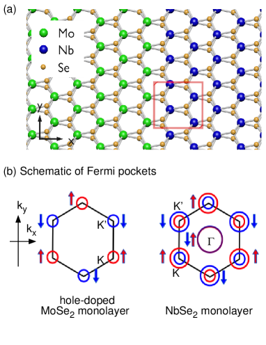
In this paper, we discuss the pseudo-spin of electrons forming Cooper pairs in the superconductor of TMDC monolayer and the effect to the electronic transport property in the lateral heterojunction of the superconducting and metallic TMDC monolayers in Fig. 1 (a). In Sec. II, we consider an effective model describing electronic states around the K and K′ valleys and analyze the pseudo-spin of electrons forming Cooper pairs in the superconducting phase. Moreover, we calculate the transmission and reflection coefficients in the lateral heterostructure and discuss the effect of pseudo-spin to these coefficients. In Sec. III, we calculate the electric conductance, which is associated with the coefficients, in the lateral heterojunction of MoSe2 and NbSe2 monolayers by using a first-principles band calculation and lattice Green’s function method. The discussion and the conclusion are given in Sec. IV and V, respectively.
II Effective model
We investigate the pseudo-spin texture of the superconducting state in TMDC monolayers.Lu et al. (2015); Xi et al. (2015); Wang et al. (2017) The Cooper pair is a spin singlet and formed of two electrons which are the time-reversal partners. In NbSe2, the Fermi level is crossing the hole band, and it arranges three Fermi pockets enclosing the , K and K′ points in the Brillouin zone as shown in Fig. 1 (b), so-called the valley degree of freedom.Habe (2019) In what follows, we consider the pair of electrons in the K and K′ valleys because the electronic states have non-trivial pseudo-spin texture in these valleys.
II.1 Electronic states in a TMDC monolayer
To analyze electronic states at the two valleys, we consider an effective model describing Dirac fermions. The effective model is represented by a Hamiltonian,
| (1) |
defined on the basis of two -orbitals, , in transition-metal atoms.Xiao et al. (2012) Here the in-plane wave number is defined with respect to the valley center, and is the valley index which is 1 in the K valley and -1 in the K′ valley. The spin-orbit coupling (SOC) is represented by the Zeeman-like term, , with the coupling constant and the spin index in the direction. The other parameters , , and are the gap energy, the Fermi energy, and the velocity, respectively. The Hamiltonian can be represented by a superposition of the identity matrix and the Pauli matrix for , , and which can be considered as a pseudo-spin operator. When the Hamiltonian is given by without the identity matrix component, we represent the axis of pseudo-spin by .
The electronic states consists of a plane wave component and a vector component expressing the pseudo-spin direction. We consider the electronic states at the Fermi level because the Cooper pair is consisting of two electrons near the level. The pseudo-spin component is represented by
| (2) |
with , where is defined by and is the Fermi wave number obtained from
| (3) |
When the electron forms a Cooper pair, the other electron is the time-reversal partner, i.e., it occupies the electronic state transformed by time-reversal operation. The partner has the same pseudo-spin component because Eq. (1) is unchanged under time-reversal operation with . Then the two electrons of Cooper pair have the same pseudo-spin, i.e., the electrons form a pseudo-spin triplet pair, although they have the opposite real spin.
The Cooper pair is always formed of equal pseudo-spin electrons but the polarizing direction changes with the Fermi energy. We consider two limits of Fermi energy; and , i.e., and , respectively. The former limit implies that the Fermi level is close to the valence band edge. In this case, the pseudo-spin is nearly independent of the wave number and has a unique polarizing axis indicated by the pseudo spin component,
| (4) |
In the latter case, the pseudo-spin varies with the wave number and has a helical texture as expressed by the vector component,
| (5) |
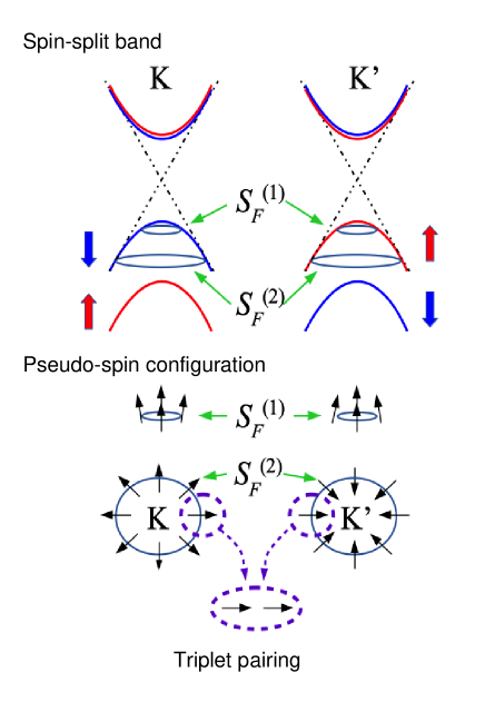
The former texture and the latter texture are schematically shown as and , respectively, in Fig. 2. In the figure, the arrows indicate the spin and pseudo-spin directions in the upper and lower panels, respectively. The direction of pseudo-spin is projected in the wave number space where gives the eigenvalue of pseudo spin for each electronic state.
II.2 Lateral heterojunction of superconducting and metallic TMDC monolayers
To discuss the effect of pseudo-spin texture, we consider the scattering problem in a lateral heterojunction of the superconducting and metallic TMDC monolayers. The lateral heterojunction is composed of two TMDC monolayers atomically bonded as a monolayer.Huang et al. (2014); Gong et al. (2014); Duan et al. (2014); Chen et al. (2015a, b); Zhang et al. (2015); He et al. (2016) When the -axis is taken to be the axis parallel to the interface of heterojunction, is preserved throughout the scattering process. Thus the conducting state can be represented by an eigen-function of , and it is a zero-energy state with respect to the Fermi level. In this section, we consider the heterojunction with zig-zag interface as shown in Fig. 1 (a), and thus we can analyze the K and K′ valleys separately.
We calculate the wave function in the junction by connecting the wave functions in the two monolayers, and thus we consider the pristine monolayers firstly. We assume that the Fermi level is crossing the lower band of Eq. (1) in both of the monolayers and that it is far away from the band edge in the superconducting monolayer. Since then is fulfilled around the Fermi level in the superconducting monolayer, the effective Hamiltonian can be approximated by that of Weyl fermion,
| (6) |
where we focus on one of spin state and put the Zeeman-like SOC in . At each , two electronic states are present if is real with
| (7) |
and they can be represented by
| (8) |
with , where the superscript indicates the sign of velocity in the -direction and it is opposite to that of . The positive velocity indicates the right going state in the right side of junction in Fig. 1 (a).
In the Bogoliubov-de Gennes (BdG) formalism, the quasi-particle state in superconductors is represented by the superposition of the electronic state and the hole state of time-reversal partner. The hole state is in the opposite valley and described by , where the Zeeman-like SOC is unchanged due to under time-reversal operation . The pseudo-spin component is the same as the electron state in Eq. (8), but the direction of velocity is inverted,
| (9) |
where the superscript also indicates the direction of velocity. The quasi-particle states in the superconducting region are the superposition of these states and described by the BdG Hamiltonian,
| (10) |
where the upper and lower components in the basis are the zero-energy electron state and the hole state of the time-reversal partner, respectively. Here is the order parameter of superconducting state where is the attractive coupling constant and indicates the Cooper pair amplitude with annihilation operator of electron in the zero energy state.
The zero-energy quasi-particle state is in the superconducting gap and thus its wave function is an evanescent wave which has a spatial dependence of with . The damping ratio can be obtained from ,
| (11) |
As discussed later, of conducting channel is much smaller than in this problem. Thus the damping ratio can be approximated by
| (12) |
where we choose the decay waves in the positive -direction. We also approximate the pseudo-spin component of the electron and hole states by those for in Eq. (8) due to . The vector component of the decay wave function is given by
| (13) |
where the first and second terms are corresponding to the upper and lower elements in Eq. (10), respectively. There are other evanescent waves consisting of only electron or hole wave function which are originated from the sates in the conduction band by solving Eq. (10) with . These evanescent waves are not responsible for the Andreev reflection process and orthogonal to other evanescent waves. Thus they can be eliminated in the calculation of scattering coefficients as discussed later.
In the metallic monolayer, the Fermi energy is assumed to be crossing the lower band near the band edge. Thus we use the original form of Hamiltonian in Eq. (1) and obtain by solving ,
| (14) |
The pseudo-spin component of electron state is represented by
| (15) |
with , where the sign indicates the direction of velocity in the direction. Then the pseudo-spin of hole state is given by .
The electronic transmission process can be described by the stationary state of scattering wave in the junction. In the metal side, there are one incident electron wave and two reflected waves in which one is the electron wave and the other is the hole wave. The amplitudes of reflected electron and hole are the normal and Andreev reflection coefficients, and , respectively. Then these wave functions satisfy the boundary condition,
| (16) |
with the decaying waves with the coefficient in the right side, where and indicate the Fermi level in the semiconducting and superconducting regions, respectively. Here is restricted in the region where conducting channels are present in the metallic region. Thus is much larger than because the Fermi pocket in the metallic monolayer is much smaller than that in the normal phase of the superconductor, . When the boundary condition is satisfied, the conservation of probability current density is fulfilled naturally because the equation for the condition is obtained by operating the velocity operator on both sides of Eq (16). Thus we use the continuous condition of momentum for calculating the coefficients,
| (17) |
We eliminate from the equations by taking the inner product with due to the orthogonality and obtain four linear equations involving four coefficients; , , , and . These four equations enable us to acquire the analytic representation of Andreev reflection coefficient,
| (18) |
with
| (19) |
where we use a relation of inner product and the condition about wave number .
This analytic result shows that the Andreev reflection is suppressed if the Fermi level gets close to the valence band top, i.e., , in the metallic region. In this case, the Fermi surface and the pseudo-spin texture is represented by in Fig. 2. The pseudo-spin is polarized in the direction and orthogonal to that in the superconducting region where the pseudo-spin is parallel to the plane. Thus, is nearly the same amplitude for the incident and reflected waves in Eq. (19). The asymptotic form in the limit is given by
| (20) |
Therefore, the Andreev reflection probability increases as a function of .
We also calculate the transmission probability in the junction with the normal phase. In this case, the reflected hole wave is absent and an electron wave with a positive velocity in the axis appears as a transmitted wave with the amplitude in the scattering problem. The stationary state satisfies the boundary condition,
| (21) |
and the continuous condition of momentum,
| (22) |
where is the transmitted wave traveling to the positive -axis. Here, the reflection coefficient is different from in the metal-superconductor heterojunction. Two linear equations are obtained by taking an inner product with the transmitted wave function and they enable us to calculate . However, is the transmission coefficient for a single channel at . Then, we correct the coefficient to obtain the transmission probability per energy by multiplying the ratio of the channel density in the superconductor to that in the metal. The ratio can be calculated by that of velocity as , where these velocities can be obtained from Eq. (6) and (1). The transmission coefficient is given by
| (23) |
with
| (24) |
This procedure is not necessary for because the channel density is unchanged between the incident and reflected waves. This analytic result indicates that the transmission probability increases with the matching of pseudo-spin between the incident and transmitted waves. The asymptotic form in the limit of is given by
| (25) |
with and .
We briefly summarize the analytic results. The Andreev reflection coefficient is proportional to the Fermi wave number in Eq. (20). This dependence is attributed to the pseudo-spin texture of electrons forming Cooper pairs. Since the pseudo-spin in the metallic TMDC reaches the fully polarization in the -axis under , the pseudo-spin projection provides a unity as a factor in Eq. (19). Thus the Andreev reflection probability is zero at and increases as a linear function of due to the change of pseudo-spin projection. In what follows, we numerically calculate the differential conductance in the lateral heterojunction of superconducting and semiconducting TMDC monolayers; NbSe2 and MoSe2, respectively. The differential conductance is associated with the Andreev reflection. We discuss the effect of pseudo-spin dependence to the differential conductance and compare it with the numerical result of conductance in the normal phase in the next section.
III Numerical calculation
III.1 First-principles band structures
We investigate the electronic structure of MoSe2 and NbSe2 in 2H-type crystal structure by using a first-principles calculation based on density functional theory (DFT). The band dispersion of MoSe2 and NbSe2 monolayers is calculated by using quantum-ESPRESSO,Giannozzi et al. (2009) a first-principles calculation code, and shown in Fig. 3.
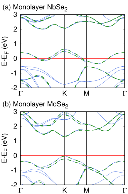
Here, we adopt the lattice constants computed by using the lattice relaxation code in quantum-ESPRESSO. The lattice parameters are Å and Å in NbSe2, and Å and Å in MoSe2, where () is the horizontal (vertical) distance between nearest neighbor transition-metal (chalcogen) atoms.Habe (2019) We apply a projector augmented wave (PAW) method to the band calculation with a generalized gradient approximation (GGA) functional including spin-orbit coupling (SOC), and adopt the cut-off energy of plane wave basis 50 Ry, and the convergence criterion 10-8 Ry. The electronic bands are classified into two groups due to the eigenvalue of mirror operation because 2H-TMDC monolayers preserve mirror reflection symmetry in the out-of-plane axis. In each band, electronic states are eigenstates of the mirror operator and characterized by the eigenvalue . Since the bands around the Fermi energy have , we consider the electronic states with in what follows.
We consider a tight-binding model to describe the local dynamics of electrons in the MoSe2 (NbSe2) monolayer where the Wannier orbitals are -orbitals in Se and -orbitals in Mo (Nb). There are six Wannier orbitals with in the primitive unit cell; , , and in Mo or Nb, and , , and in Se. Here is the superposition of -orbitals in the top Se and the bottom Se, and , respectively. The hopping integrals between these orbitals and on-site potential are computed from the first-principles bands in Fig. 3 by using Wannier90Mostofi et al. (2008). Since the DFT calculation underestimates the band gap in semiconductors,Qiu et al. (2013); Kim and Son (2017); Drüppel et al. (2018) we use the charge density as a parameter instead of the Fermi energy. The charge density can be controlled by using gates in experiments.Zhang et al. (2012) Each band splits into two due to the large spin-orbit coupling because of inversion symmetry-breaking in the crystal structure. The effect of spin-orbit coupling is included as spin-dependent hopping integrals in the tight-binding Hamiltonian. The spin-orbit coupling acts as a -dependent Zeeman field in the axis due to mirror reflection symmetry. Thus, electronic states split into two spin states, where the spin polarization direction is parallel to the axis. The tight-binding model reproduces the first-principles bands as shown in Fig. 3. Here, the dashed lines are bands calculated by using the tight-binding model.
III.2 Bogoliubov-de Gennes Hamiltonian
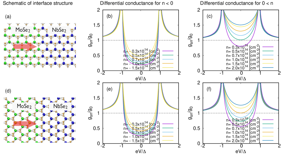
Electronic states in the junction are described by a tight-binding model consisting of that of pristine MoSe2 and NbSe2 monolayers, where we consider two types of junctions with the zig-zag interface and the armchair interface as shown in Fig. 4 (a) and (c). The hopping matrix through the interface is assumed to be that for MoSe2 because the difference of computed hopping matrix is smaller than 5 meV between MoSe2 and NbSe2. In this paper, we consider non-zero charge density induced by a homogeneous gate. The Fermi energy aligns to that of the pristine monolayers with the distance far from the interface where it is calculated from
| (26) |
where is the energy dispersion of band in Fig. 3. The bands in both of the monolayers are aligned for the Fermi energy to be matched. In general, the potential fluctuation emerges near the interface of two monolayers and can be a contact resistance but we omit the effect for simplicity. We also assume the atomically commensurate interfaceLi et al. (2015); Gong et al. (2014) because a previous study show that a flat and commensurate heterojunction has a local minimum of free-energy even in the presence of mismatch in the lattice constant.Xie et al. (2018) This allows us to use one-dimensional tight-binding Hamiltonian with a wave number parallel to the interface under the periodic boundary condition. We represent the wave number by with an integer , where is the perimeter along the axis.
The tight-binding Hamiltonian for each is obtained by using Fourier transformation in the axis,
| (27) |
where the on-site potential and the hopping matrix are matrix, and is a vector of the annihilation operators with on the site where the basis is defined by all the forty eight orbitals including the spin degree of freedom in the unit cell as shown in Fig. 1. Here, we adopt the hopping integrals computed from the first-principles bands of MoSe2 (NbSe2) as the on-site potential and the hopping matrix for ().
We consider the superconducting states in NbSe2 by using Bogoliubov-de Gennes (BdG) theory. In this formalism, quasi-particle states are described by the BdG Hamiltonian. The on-site potential and hopping matrix are defined on the basis of electron and hole states in the same manner as Eq. (10), where is the superconducting gap, is the identity matrix in the basis of , and is the Pauli matrix for the spin. Here, the basis is the Nambu basis where the spin axis is chosen to be parallel to the axis. The superconducting gap can be estimated by with the transition temperature and Euler’s constant according to Bardeen Cooper Schrieffer theory. The transition temperature is obtained as K for monolayer NbSe2 experimentally.Lu et al. (2015); Wang et al. (2017) In a bilayer NbSe2, the transition temperature changes with the gate voltageXi et al. (2016) but we omit a change of transition temperature by gating in this calculation. Since the superconducting gap is absent in MoSe2 region, we set for .
In the representation, incident electrons are reflected at the interface of the junction as far as the electron has an energy in the superconducting gap of NbSe2 monolayer. We briefly recall the discussion about the reflection process in the superconductor-metal junction in Sec. II. There are two types of reflection processes classified by the charge of reflected particle. The normal reflection means that the incident electron (hole) is reflected and goes back as an electron (hole). The other is called Andreev reflection where the incident electron (hole) changes into a hole (electron) coming back.Blonder et al. (1982) The Andreev reflection process is understood as that an incident electron transmits in the superconductor by forming a Cooper pair, the pair of electron bounded by an attractive force, with another electron which leaves a hole near the interface. Thus, the charge transport property in the metal-superconductor junction is associated with the Andreev reflection. The differential conductance , which is defined by using the electric current and the source-drain bias voltage , is given by
| (28) |
where and are the reflection coefficients for the normal reflection process and the Andreev reflection process of electrons in the conduction channel .Blonder et al. (1982); Takane and Ebisawa (1992)
We study the electronic transmission between the MoSe2 and NbSe2 monolayers by using the two-terminal lattice Green’s function method. The heterojunction can be separated into two lead-regions and an interface region. In the leads, the electronic states can be represented by , where indicates the position. The phase factor and the state vector at an energy are described by
| (29) |
In the semiconductor, the eigenstates can be separated into those for electrons, , and holes, , because of . The reflection coefficients are computed from the lattice Green’s function methodAndo (1991); Lewenkopf and Mucciolo (2013); Habe and Koshino (2015, 2016) in the multi-orbital tight-binding model in Eq. (LABEL:eq_tight-binding_model) for incident electron states. The Andreev and normal reflection coefficients are distinguished by the amplitude of reflected waves, and , respectively.
III.3 Numerical results
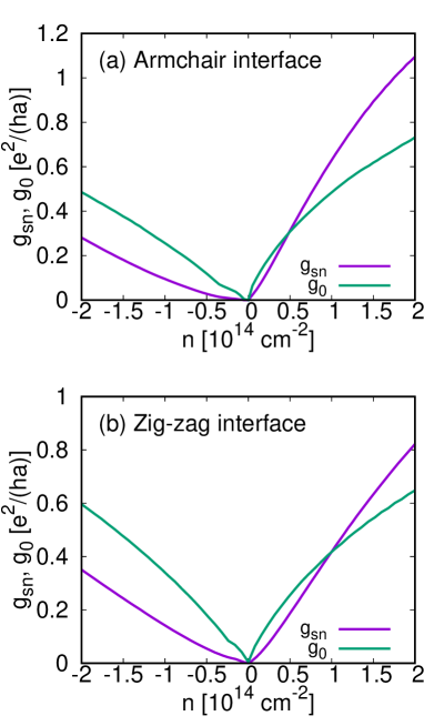
We show the differential conductance as a function of source-drain bias voltages in Fig. 4. The vertical and horizontal axes indicate the normalized differential conductance by the conductance in the normal phase of NbSe2 and the source-drain voltage , respectively. Here, the bias voltage is normalized by the gap energy , and implies that incident electrons have the energy matched to the edge of quasi-particle band. In the electron-doped hetelojunction , the normalized differential conductance is suppressed and not sensitive to the charge density and the structure of interface, the armchair structure in (b) and the zig-zag structure in (e). The differential conductance for , on the other hand, strongly depends on the charge density, and it exceeds the normal conductance with increase in . This result indicates that the Andreev reflection is enhanced with increase in . The interface structure of heterojunction also quantitatively changes the differential conductance as shown in (c) and (f), and the armchair interface enhances it for hole-doped heterojunctions, . We also plot the dependence of the differential conductance in the superconducting phase and the normal conductance in the normal phase at in Fig. 5. In the case of , the normal conductance is always larger than the differential conductance for both of the interface structures.
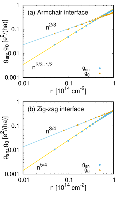
We also show the log-log scale plot of the dependence for the hole-doped heterojunction in Fig. 6. The numerical data align on a line in the form of in both cases of and . The gradient of lines is corresponding to the power index . Although the index changes with the interface structure, the difference of the index between and is a half regardless of the interface. This difference causes the crossover from to with an increase of in Fig. 5.
The analytic formula in Sec. II also provides the difference consistent with the numerical result. The Andreev reflection probability and the transmission probability are represented by functions of which is proportional to because of the quadratic dispersion and the constant density of state. Since is fulfilled inside the superconducting gap, the power index of with respect to is that of plus a half. Here the half is attributed to the integration with respect to for calculating from at each . The transmission probability has the power index of plus a half. Therefore, it is confirmed that the difference of power indexes is a half by using the analytic results in Eq. (20) and (25) in Sec. II.
IV Discussion
Finally, we consider the mismatch of power index between the numerical and analytic results. It is attributed to the simplification of band structure of NbSe2 in the analytic formulation. The Fermi pocket in TMDCs is not isotropic around the K, K′, and points and warping due to three-fold rotation symmetry of the crystal structure. The trigonal warping could change the wave vector dependence of Andreev reflection and transmission coefficients. Moreover, the heterostructure with the Armchair interface allows the electronic transmission between the K or K′ valley in MoSe2 and the valley in NbSe2 as discussed in our previous paper.Habe (2019) This also can fluctuates the power index of and . However, the difference of power index can remain robust even if the two types of interface are coexisting in the realistic heterojucntion. Therefore, this crossover can be an experimental proof of the pseudo-spin triplet Cooper pair in the superconducting NbSe2 monolayer.
V Conclusion
In this paper, we have analyzed the pseudo-spin texture of electrons forming spin singlet Cooper pairs in superconducting TMDC monolayers and shown that the parallel pseudo-spin pair is realized in the superconducting monolayer. The pseudo-spin polarizing direction varies with the direction and magnitude of the wave number. Forming a heterojunction of superconducting and metallic monolayers, the pseudo-spin direction affects the electronic transmission and reflection probability. The Andreev reflection, the electronic transmission with transforming a Cooper pair, vanishes in the limit of Fermi energy crossing the valence band edge. We numerically calculated the conductance in the normal phase and the superconducting phase at each charge density. We found that the conductance decreases with changing the phase from the normal one to the superconducting one in the low charge density region but it increases in the high charge density region. This charge density dependence is attributed to the difference of pseudo-spin polarizing axis in the two TMDC monolayers, and it can be a proof of parallel pseudo-spin Cooper pair.
References
- Helveg et al. (2000) S. Helveg, J. V. Lauritsen, E. Lægsgaard, I. Stensgaard, J. K. Nørskov, B. S. Clausen, H. Topsøe, and F. Besenbacher, Phys. Rev. Lett. 84, 951 (2000).
- Mak et al. (2010) K. F. Mak, C. Lee, J. Hone, J. Shan, and T. F. Heinz, Phys. Rev. Lett. 105, 136805 (2010).
- Coleman et al. (2011) J. N. Coleman, M. Lotya, A. O’Neill, S. D. Bergin, P. J. King, U. Khan, K. Young, A. Gaucher, S. De, R. J. Smith, I. V. Shvets, S. K. Arora, G. Stanton, H.-Y. Kim, K. Lee, G. T. Kim, G. S. Duesberg, T. Hallam, J. J. Boland, J. J. Wang, J. F. Donegan, J. C. Grunlan, G. Moriarty, A. Shmeliov, R. J. Nicholls, J. M. Perkins, E. M. Grieveson, K. Theuwissen, D. W. McComb, P. D. Nellist, and V. Nicolosi, Science 331, 568 (2011).
- Lee et al. (2012) Y.-H. Lee, X.-Q. Zhang, W. Zhang, M.-T. Chang, C.-T. Lin, K.-D. Chang, Y.-C. Yu, J. T.-W. Wang, C.-S. Chang, L.-J. Li, and T.-W. Lin, Adv. Mater. 24, 2320 (2012).
- Dong and Kuljanishvili (2017) R. Dong and I. Kuljanishvili, Journal of Vacuum Science & Technology B 35, 030803 (2017).
- Lu et al. (2015) J. M. Lu, O. Zheliuk, I. Leermakers, N. F. Q. Yuan, U. Zeitler, K. T. Law, and J. T. Ye, Science 350, 1353 (2015).
- Xi et al. (2015) X. Xi, L. Zhao, Z. Wang, H. Berger, L. Forró, J. Shan, and K. F. Mak, Nature Nanotechnology 10, 765 (2015).
- Wang et al. (2017) H. Wang, X. Huang, J. Lin, J. Cui, Y. Chen, C. Zhu, F. Liu, Q. Zeng, J. Zhou, P. Yu, X. Wang, H. He, S. H. Tsang, W. Gao, K. Suenaga, F. Ma, C. Yang, L. Lu, T. Yu, E. H. T. Teo, G. Liu, and Z. Liu, Nature Communications 8, 394 (2017).
- Ugeda et al. (2015) M. M. Ugeda, A. J. Bradley, Y. Zhang, S. Onishi, Y. Chen, W. Ruan, C. Ojeda-Aristizabal, H. Ryu, M. T. Edmonds, H.-Z. Tsai, A. Riss, S.-K. Mo, D. Lee, A. Zettl, Z. Hussain, Z.-X. Shen, and M. F. Crommie, Nature Physics 12, 92 (2015).
- Tang et al. (2017) S. Tang, C. Zhang, D. Wong, Z. Pedramrazi, H.-Z. Tsai, C. Jia, B. Moritz, M. Claassen, H. Ryu, S. Kahn, et al., Nature Physics 13, 683 (2017).
- Kershaw et al. (1967) R. Kershaw, M. Vlasse, and A. Wold, Inorganic Chemistry 6, 1599 (1967).
- Möckli and Khodas (2018) D. Möckli and M. Khodas, Phys. Rev. B 98, 144518 (2018).
- Aliabad and Zare (2018) M. R. Aliabad and M.-H. Zare, Phys. Rev. B 97, 224503 (2018).
- Sohn et al. (2018) E. Sohn, X. Xi, W.-Y. He, S. Jiang, Z. Wang, K. Kang, J.-H. Park, H. Berger, L. Forró, K. T. Law, et al., Nat Mater 17, 504 (2018).
- Shaffer et al. (2019) D. Shaffer, J. Kang, F. J. Burnell, and R. M. Fernandes, arXiv:1905.01063 (2019).
- Glodzik and Ojanen (2019) S. Glodzik and T. Ojanen, arXiv:1905.01063 (2019).
- Xiao et al. (2012) D. Xiao, G.-B. Liu, W. Feng, X. Xu, and W. Yao, Phys. Rev. Lett. 108, 196802 (2012).
- Shan et al. (2013) W.-Y. Shan, H.-Z. Lu, and D. Xiao, Phys. Rev. B 88, 125301 (2013).
- Zibouche et al. (2014) N. Zibouche, A. Kuc, J. Musfeldt, and T. Heine, Annalen der Physik 526, 395 (2014).
- Habe and Koshino (2017) T. Habe and M. Koshino, Phys. Rev. B 96, 085411 (2017).
- Cappelluti et al. (2013) E. Cappelluti, R. Roldán, J. A. Silva-Guillén, P. Ordejón, and F. Guinea, Phys. Rev. B 88, 075409 (2013).
- Habe (2019) T. Habe, arXiv:1904.0179 (2019).
- Huang et al. (2014) C. Huang, S. Wu, A. M. Sanchez, J. J. P. Peters, R. Beanland, J. S. Ross, P. Rivera, W. Yao, D. H. Cobden, and X. Xu, Nature Materials 13, 1096 (2014).
- Gong et al. (2014) Y. Gong, J. Lin, X. Wang, G. Shi, S. Lei, Z. Lin, X. Zou, G. Ye, R. Vajtai, B. I. Yakobson, H. Terrones, M. Terrones, B. Tay, J. Lou, S. T. Pantelides, Z. Liu, W. Zhou, and P. M. Ajayan, Nature Materials 13, 1135 (2014).
- Duan et al. (2014) X. Duan, C. Wang, J. C. Shaw, R. Cheng, Y. Chen, H. Li, X. Wu, Y. Tang, Q. Zhang, A. Pan, J. Jiang, R. Yu, Y. Huang, and X. Duan, Nature Nanotechnology 9, 1024 (2014).
- Chen et al. (2015a) K. Chen, X. Wan, W. Xie, J. Wen, Z. Kang, X. Zeng, H. Chen, and J. Xu, Advanced Materials 27, 6431 (2015a).
- Chen et al. (2015b) K. Chen, X. Wan, J. Wen, W. Xie, Z. Kang, X. Zeng, H. Chen, and J.-B. Xu, ACS Nano 9, 9868 (2015b).
- Zhang et al. (2015) X.-Q. Zhang, C.-H. Lin, Y.-W. Tseng, K.-H. Huang, and Y.-H. Lee, Nano Letters 15, 410 (2015).
- He et al. (2016) Y. He, A. Sobhani, S. Lei, Z. Zhang, Y. Gong, Z. Jin, W. Zhou, Y. Yang, Y. Zhang, X. Wang, B. Yakobson, R. Vajtai, N. J. Halas, B. Li, E. Xie, and P. Ajayan, Advanced Materials 28, 5126 (2016).
- Giannozzi et al. (2009) P. Giannozzi, S. Baroni, N. Bonini, M. Calandra, R. Car, C. Cavazzoni, D. Ceresoli, G. L. Chiarotti, M. Cococcioni, I. Dabo, A. Dal Corso, S. de Gironcoli, S. Fabris, G. Fratesi, R. Gebauer, U. Gerstmann, C. Gougoussis, A. Kokalj, M. Lazzeri, L. Martin-Samos, N. Marzari, F. Mauri, R. Mazzarello, S. Paolini, A. Pasquarello, L. Paulatto, C. Sbraccia, S. Scandolo, G. Sclauzero, A. P. Seitsonen, A. Smogunov, P. Umari, and R. M. Wentzcovitch, J. Phys.: Condens. Matter 21, 395502 (2009).
- Mostofi et al. (2008) A. A. Mostofi, J. R. Yates, Y.-S. Lee, I. Souza, D. Vanderbilt, and N. Marzari, Computer Physics Communications 178, 685 (2008).
- Qiu et al. (2013) D. Y. Qiu, F. H. da Jornada, and S. G. Louie, Phys. Rev. Lett. 111, 216805 (2013).
- Kim and Son (2017) S. Kim and Y.-W. Son, Phys. Rev. B 96, 155439 (2017).
- Drüppel et al. (2018) M. Drüppel, T. Deilmann, J. Noky, P. Marauhn, P. Krüger, and M. Rohlfing, Phys. Rev. B 98, 155433 (2018).
- Zhang et al. (2012) Y. Zhang, J. Ye, Y. Matsuhashi, and Y. Iwasa, Nano Letters 12, 1136 (2012).
- Li et al. (2015) M.-Y. Li, Y. Shi, C.-C. Cheng, L.-S. Lu, Y.-C. Lin, H.-L. Tang, M.-L. Tsai, C.-W. Chu, K.-H. Wei, J.-H. He, W.-H. Chang, K. Suenaga, and L.-J. Li, Science 349, 524 (2015).
- Xie et al. (2018) S. Xie, L. Tu, Y. Han, L. Huang, K. Kang, K. U. Lao, P. Poddar, C. Park, D. A. Muller, R. A. DiStasio, and J. Park, Science 359, 1131 (2018), https://science.sciencemag.org/content/359/6380/1131.full.pdf .
- Xi et al. (2016) X. Xi, H. Berger, L. Forró, J. Shan, and K. F. Mak, Phys. Rev. Lett. 117, 106801 (2016).
- Blonder et al. (1982) G. E. Blonder, M. Tinkham, and T. M. Klapwijk, Phys. Rev. B 25, 4515 (1982).
- Takane and Ebisawa (1992) Y. Takane and H. Ebisawa, Journal of the Physical Society of Japan 61, 1685 (1992), https://doi.org/10.1143/JPSJ.61.1685 .
- Ando (1991) T. Ando, Phys. Rev. B 44, 8017 (1991).
- Lewenkopf and Mucciolo (2013) C. Lewenkopf and E. Mucciolo, J Comput Electron 12, 203 (2013).
- Habe and Koshino (2015) T. Habe and M. Koshino, Phys. Rev. B 91, 201407 (2015).
- Habe and Koshino (2016) T. Habe and M. Koshino, Phys. Rev. B 93, 075415 (2016).