Tailored nanoscale plasmon-enhanced vibrational electron spectroscopy
Abstract
Vibrational optical spectroscopies can be enhanced by surface plasmons to reach molecular-sized limits of detection and characterization. The level of enhancement strongly depends on microscopic details of the sample that are generally missed by macroscopic techniques. Here we investigate phonons in h-BN by coupling them to silver-nanowire plasmons, whose energy is tuned by modifying the nanowire length. Specifically, we use electron beam milling to accurately and iteratively change the nanowire length, followed by electron energy-loss spectroscopy to reveal the plasmon-enhanced vibrational features of h-BN. This allows us to investigate otherwise hidden bulk phonons and observe strong plasmon-phonon coupling. The new milling-and-spectroscopy technique holds great potential for resolving vibrational features in material nanostructures.
Vibrational spectroscopy is key in a wide range of research areas and technological applications, from molecular fingerprinting to fundamental solid-state physics Zenobi (2017); Verma (2017). The discovery that plasmonic structures can increase the measured vibrational signal has driven the development of ultra-sensitive analytical techniques capable of reaching single-molecule detection, such as in surface-enhanced Raman spectroscopy Fleischmann et al. (1974); Nie and Emory (1997) (SERS) and surface-enhanced infrared absorption Osawa and Ikeda (1991) (SEIRA). Typically, plasmonic structures are designed in advance and molecules are randomly dispersed over them, leading to strongly enhanced signals associated with those sitting on the so-called hotspotsNie and Emory (1997). Alternatively, a metallic tip can be scanned over a sample to induce SERS locally, leading to chemical mapping at sub-molecular scales, a technique known as tip-enhanced Raman scattering Sonntag et al. (2014) (TERS).
Vibrational electron energy-loss spectroscopy (EELS) has been performed for decades mainly as a surface technique Ibach and Mills (1982) using wide beams with poor spatial resolution. The recent development of a new family of electron monochromators Krivanek et al. (2009) has allowed vibration mode measurements to be performed based on EELS Krivanek et al. (2014); Lagos et al. (2017); Senga et al. (2018) down to atomic spatial resolution in bulk materialsHage et al. (2019). Unfortunately, the signal-to-noise ratio of vibrational EELS is low for materials that are sensitive to the electron beam, thus imposing a lower bound on the volume necessary for analysis. This jeopardizes the high resolution mapping of fragile materials, such as organic molecules Rez et al. (2016). Recently, theoretical studies Neubrech et al. (2008); Konecna et al. (2018); Kordahl and Dwyer (2019) have proposed the use of infrared plasmonic fields to develop a new form of enhanced vibrational EELS which would overcome these limitations by making the molecules interact with the beam at a distance mediated by plasmons extended in a nanoparticle.
Here, we demonstrate plasmon-enhanced vibrational electron spectroscopy (PEVES) through the tailored coupling of plasmon resonances in metallic nanowires to phonon modes in h-BN thin flakes. Coupling is achieved by continuously shifting the energies of the plasmon modes of micrometer-long metallic nanowires (Fig. S1) using electron-beam controlled milling to bring them into resonance with specific h-BN vibrational modes (Fig. S2). We reveal three new effects when a plasmon-phonon resonance is encountered: 1) strong coupling between surface phonons and plasmons; 2) enhancement of the bulk vibrational EELS signal; and 3) emergence of previously geometry-forbidden dark phonon modes.
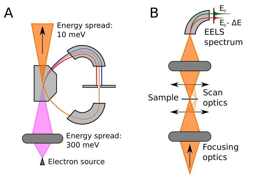
EELS measures the distribution of energy losses experienced by free electrons when interacting with a target Egerton (1996). The energy resolution is determined by the energy spread of the electron source, typically 250 meV for a cold field emitter source. This resolution can be improved down to a few meV using an electron monochromator (Fig. S3). To achieve subnanometer spatial resolution, the electron monochromator can be coupled to an electron microscope (Fig. S3). Finally, an electron spectrometer is used to acquire the spectrum of the electron beam after interaction with the sample. Here, we use such a setup implemented on a NION Hermes scanning transmission microscope (STEM), see Methods.
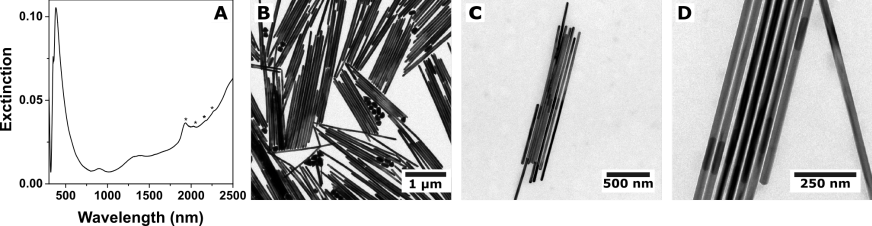
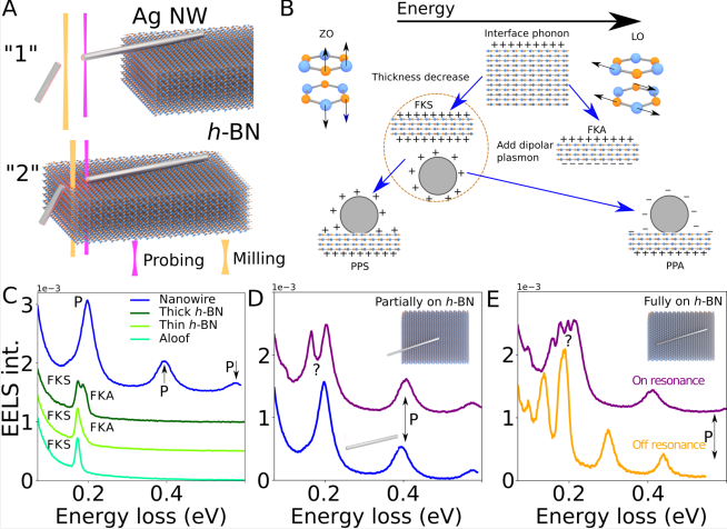
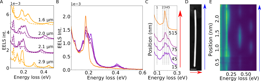
The plasmonic silver metallic nanowires were synthesized by chemical seeded growth as detailed elsewhere Mayer et al. (2015) (Fig. 1A) and subsequently deposited, either entirely (configuration (1)) or partially (configuration (2)), on an h-BN substrate Taniguchi and Watanabe (2007). In theory, extended h-BN possesses a variety of infrared-active either transverse optical (TO) or longitudinal optical (LO) phonons. Due to the h-BN anisotropy, TO and LO phonons may possess different energies depending on whether they are polarized out- or in-plane Geick et al. (1966). Bulk EELS is therefore very dependent on the orientation of the electron to the h-BN crystallographic orientation. Indeed, when the electron propagates along the [0001] h-BN direction, mainly the in-plane LO bulk mode is excited, while the out-of-plane modes can only be excited in a tilted configuration. Thin h-BN substrates sustain additionally two surface phonon modes: the charge-symmetric (FKS) and charge-antisymmetric (FKA) Fuchs-Kliewer modes, whose energies disperse as a function of thickness. A qualitative sketch of the energy hierarchy of the different modes discussed in the text is presented in Fig. 1B. For very thin substrates, the former (FKS) arises at the in-plane TO phonon energy (around 169 meV) and the later (FKA) at the out-of-plane LO phonon energy (around 198 meV). In EELS experiments, the FKS (resp. FKA) energy varies between the TO (resp. LO) energy and that of the h-BN interface phonon (around 195 meV). Also, the FKA intensity is usually much smaller than that of the FKS Batson and Lagos (2017); Lourenço-Martins and Kociak (2017), see (Fig. 1C, green curves). The FK modes usually overshadow the bulk modes, at least for the thickness range probed in this study (50-100 nm). Nanowire plasmons of well-defined energy are produced due to confinement, leading to modes that can be classified as dipolar, quadrupolar, etc., depending on the number of nodes in the induced-charge along the nanowire length. In the nanowire cross-section, the charge distribution is homogeneous. EELS is extremely sensitive to surface plasmon modes and reveals their nearly uniform energy spacing (Fig. 1C). Their energies are roughly proportional to the inverse of the nanowire length, which thus becomes a perfect parameter to tune the nanowire plasmon energies. Finally, we note that both surface plasmons and surface phonons (FK modes) can also be excited in a geometry where the beam does not directly hit the sample (”aloof geometry”) Nelayah et al. (2007); Krivanek et al. (2014); Lagos et al. (2017).
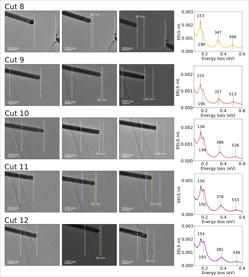
Plasmon-phonon interaction was probed initially using a sample configuration (”1” in Fig. 1A) where only surface phonons interact with surface plasmons, to avoid any potential overlap between surface and bulk effects. In this geometry, long silver nanowires with only one tip placed on different volumes of h-BN were modified in length by electron milling in order to bring their dipolar plasmon into and then out of resonance with respect to the h-BN FK modes.
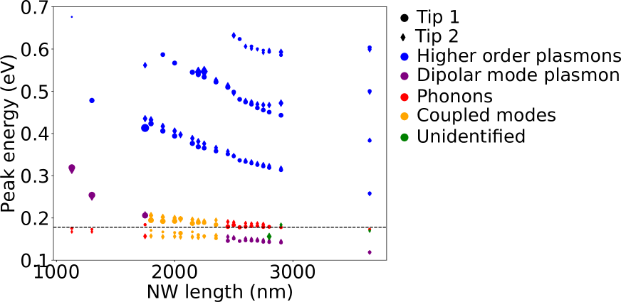
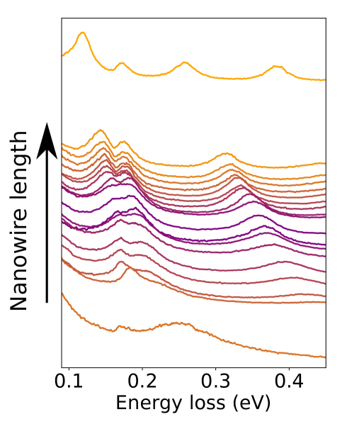
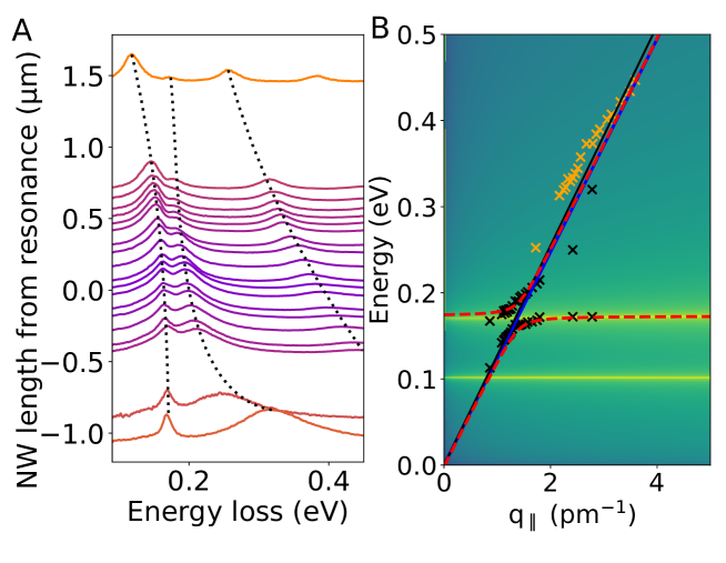
When their energies differ by more than meV, phonons and surface plasmons do not interact (Figs. 1D, blue curve, and 2A, orange curves). As the nanowire length is shortened, the dipolar plasmon energy approaches that of the FKS mode. Close to resonance, a second peak is observed at the nanowire tip in vacuum, away from h-BN, at an energy close to 180 meV (Figs. 1D and 2A, purple curves). The two peaks do not cross each other as the nanowire length is varied, exhibiting a minimum splitting of 37 meV (average splitting in the -m nanowire length range), comparable to the full width at half maximum of the two peaks (between 30 and 40 meV). The energy of the first peak continues to increase for nanowire lengths shorter than m. However, it does not disperse proportionally to the inverse of the nanowire length , as expected for plasmons on long metallic nanowires. This is in contrast with the higher order plasmon modes that indeed disperse as expected as (Fig. S4). This behavior is nicely reproduced by numerical calculations (Fig. 2B). Peak-splitting was observed to vary between nanowires (in the 0-52 meV range in Figs. S5-8).
These observations indicate strong coupling between the dipolar surface plasmon and the FKS mode. For small detuning, the two peaks cannot be assigned as either a plasmon or a phonon, but rather as hybrid plasmon-phonon (PP) modes, either charge-symmetric (low-energy, PPS) or charge-antisymmetric (high-energy, PPA), see Fig. 1B. After the anticrossing, the nature of the modes is inverted, as expected for strong coupling: the lower (higher) energy peak changes continuously from the plasmon (phonon) to the phonon (plasmon) mode. Strong coupling evidences a coherent field across the whole nanowire, as its signature is observed at a region of the nanowire where no h-BN is present and the aloof signal from h-BN without nanowire is not experimentally detectable. In fact, the coupled peaks are only observed where the dipolar mode is measurable, close to the nanowire tips (Fig. S9). This can be more clearly observed in a line profile of the hyperspectral image going from the nanowire tip in vacuum to the region supported on thin h-BN (Fig. S9). As the electron beam is moved away from the nanowire tip, the two coupled modes lose intensity. When it approaches h-BN, the lower energy FKS mode is observed at an intermediate energy between the two coupled modes. Finally, with the electron beam on h-BN, both FK modes are revealed.
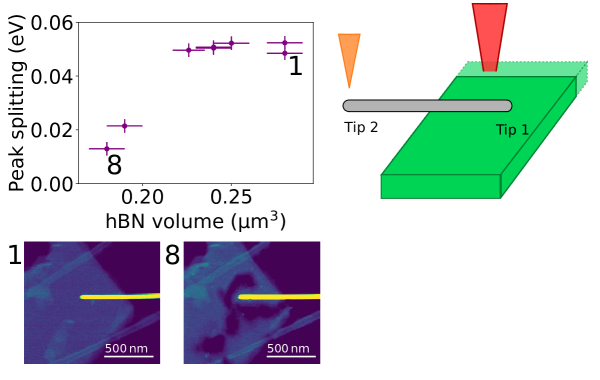
The energy splitting due to coupling depends on the amount of h-BN contained inside the modal volume of the dipole surface plasmon Konecna et al. (2018). For small quantities, no splitting is observed (Fig. S6). For intermediate amounts, a 17 meV splitting is observed in some measurements (Fig. S7). The largest observed splitting in this study is 52 meV Fig. S8. These results support the hypothesis that the volume of h-BN within the dipole surface plasmon modal volume determines the splitting of the two strongly-coupled peaks, starting from a large volume of h-BN, where the splitting continuously decreases from 52 meV down to 12 meV (Fig. S8). We note that a removal of h-BN performed only within 500 nm of the nanowire tip did modify the splitting, while removal farther away did not affect the splitting, again indicating that the coupling is mediated by the overlap of the plasmon field lines and h-BN.
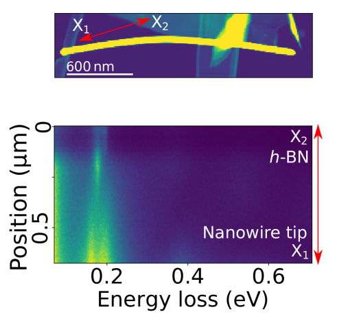
The above-described behavior is observed at the nanowire tip lying on h-BN, but with the complicating factor that h-BN losses are also present. To understand the signal when h-BN is present, a second sample geometry (”2” in Fig. 1A), in which the nanowire is lying completely on an homogeneous piece of h-BN, was used. The presence of plasmons with energies away from the phonon energies (Fig. 1E, orange curve) does not affect the phonon spectra. Close to a plasmon-phonon resonance, the spectra change substantially (Fig. 1E, purple curve and S10), with the appearance of multiple peaks at 100 meV, 161 meV, 177 meV, 197 meV, and 217 meV (Fig.. 3A, B and marked 1 through 5, respectively in C). This multiple peak structure is reproduced by theoretical calculations (dashed curves in Fig. 3A). The 161 meV and 217 meV modes do disperse with nanowire length, and can be safely attributed to the PPS and PPA modes (their dispersion is confirmed by numerical calculations shown in Fig. S11). Three peaks are left to be identified (100, 177, and 197 meV). For the 2.1 m long nanowire, peak energies do not change as a function of the distance away from the nanowire tip at which they are probed (Fig. 3B-C and S12), but their intensities do.
The 177 meV mode intensity increases away from the nanowire surface, while the four others vanish (Fig. 3B-C). The 177 meV mode can be interpreted as the FKS, excited in an aloof-like configuration when the beam is close to the nanowire tip. The probability of exciting it obviously decreases as the PPA and PPS, which are hybrid plasmon-FKS modes, are more intensely excited close to the nanowire tip.
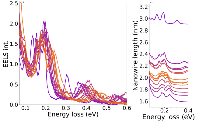
Away from the influence area of the dipolar mode, the vanishing of the PPA and PPS signals is expected, as they are formed where the plasmon field lines are intense enough. The 100 and 197 meV peaks show similar spatial variation, indicating that they have a common origin. The first of these energies matches that of the ZO normal mode Serrano et al. (2007) (a longitudinal optical phonon polarized along the anisotropy axis), and the second one corresponds well with that of the LO mode polarized perpendicular to the anisotropy axis (see a schematics on Fig. 1B). As these modes should not be observed in the sample geometry here considered, their observation can only be explained by their coupling to the plasmon mode, which enhances them. The enhancement is maximal within 30 nm of the nanowire surface, which strengthens the link to the surface plasmon.
In summary, two main effects are observed: the possibility to detect a bulk phonon mode (the ZO mode), whose excitation, in the absence of a nanowire, is geometry-forbidden, and an extreme enhancement of the LO and ZO modes. The magnitude of the enhancement cannot be quantified, as in the absence of nanowire both modes are not experimentally detectable.
Interestingly, the enhancement is not homogeneous across the whole nanowire: both ZO and LO modes are enhanced at the tips, while only the ZO mode is enhanced at the center (Fig. 3D,E). We attribute this effect to the dependence of the enhancement on the direction of the plasmon electric field, which changes along the nanowire length: close to the tips the field has substantial projections on all directions, while at the nanowire center it is mostly oriented parallel to the metal surface. Some phonon modes are only observed when the electric field has a component out of the h-BN plane. The PPS and PPA peaks are visible close to the nanowire tips (left and right of Fig. 3D), while others appear along the entire nanowire (Fig. 3D, ZO peak). In this respect, the symmetry of the plasmon electric field mode provides additional information about the phonons with which it interacts.
Controlled coupling between plasmon and phonon modes with precision below 10 meV opens the way to a new form of plasmon-enhanced vibrational spectroscopy (PEVES). Plasmon modes are highly localized in space, leading to stronger enhancement effects in volumes of the order of nm3 Neubrech et al. (2008); only a technique with sub-10 nm spatial resolution can exploit this high localization. The plasmonic enhancement has the additional benefit that smaller sample volumes can be probed than with regular EELS. More advanced sample designs should allow fingerprinting of molecular vibration modes. For example, one could produce dedicated slots in metallic structures, each of them containing different analytes; or a movable metallic tip could be added to the microscope holder (as demonstrated in previous workOhnishi et al. (1998)) to selectively enhance the vibrational modes along a molecule. Sequencing of DNA strands also appears as a possible application of PEVES by scanning both the tip and the electron beam.
Acknowledgements.
This project has received funding from the european union’s horizon 2020 research and innovation programme under grant agreement no 823717.This work has received support from the National Agency for Research under the program of future investment TEMPOS-CHROMATEM with the Reference No. ANR-10-EQPX-50. We acknowledge support from Spanish MINECO (MAT2017-88492-R and SEV2015-0522), ERC (Advanced Grants 789104-eNANO and 4DBIOSERS, AdG 787510), the Catalan CERCA Program, and Fundació Privada Cellex. The authors acknowledge Christoph Hanske for help in the nanowire sample preparation.References
- Zenobi (2017) R. Zenobi, “Introduction: Vibrational nanoscopy,” (2017).
- Verma (2017) P. Verma, Chem. Rev. 117, 6447 (2017).
- Fleischmann et al. (1974) M. Fleischmann, P. J. Hendra, and A. J. McQuillan, Chem. Phys. Lett. 26, 163 (1974).
- Nie and Emory (1997) S. Nie and S. R. Emory, Science 275, 1102 (1997).
- Osawa and Ikeda (1991) M. Osawa and M. Ikeda, J. Phys. Chem. 95, 9914 (1991).
- Sonntag et al. (2014) M. D. Sonntag, E. A. Pozzi, N. Jiang, M. C. Hersam, and R. P. Van Duyne, J. Phys. Chem. Lett. 5, 3125 (2014).
- Ibach and Mills (1982) H. Ibach and D. L. Mills, Electron energy loss spectroscopy and surface vibrations (Academic Press, San Diego, 1982).
- Krivanek et al. (2009) O. L. Krivanek, J. P. Ursin, N. J. Bacon, G. J. Corbin, N. Dellby, P. Hrncirik, M. F. Murfitt, C. S. Own, and Z. S. Szilagyi, Philos. Trans. Royal Soc. A 367, 3683 (2009).
- Krivanek et al. (2014) O. L. Krivanek, T. C. Lovejoy, N. Dellby, T. Aoki, R. W. Carpenter, P. Rez, E. Soignard, J. Zhu, P. E. Batson, M. J. Lagos, R. F. Egerton, and P. A. Crozier, Nature 514, 209 (2014).
- Lagos et al. (2017) M. J. Lagos, A. Trügler, U. Hohenester, and P. E. Batson, Nature 543, 529 (2017).
- Senga et al. (2018) R. Senga, K. Suenaga, P. Barone, S. Morishita, F. Mauri, and T. Pichler, arXiv:1812.08294 (2018).
- Hage et al. (2019) F. S. Hage, D. M. Kepaptsoglou, Q. M. Ramasse, and L. J. Allen, Phys. Rev. Lett. 122, 016103 (2019).
- Rez et al. (2016) P. Rez, T. Aoki, K. March, D. Gur, O. L. Krivanek, N. Dellby, T. C. Lovejoy, S. G. Wolf, and H. Cohen, Nat. Commun. 7, 10945 (2016).
- Neubrech et al. (2008) F. Neubrech, A. Pucci, T. W. Cornelius, S. Karim, A. García-Etxarri, and J. Aizpurua, Phys. Rev. Lett. 101, 157403 (2008).
- Konecna et al. (2018) A. Konecna, T. Neuman, J. Aizpurua, and R. Hillenbrand, ACS Nano 12, 4775 (2018).
- Kordahl and Dwyer (2019) D. Kordahl and C. Dwyer, Phys. Rev. B 99, 104110 (2019).
- Egerton (1996) R. F. Egerton, Electron Energy-Loss Spectroscopy in the Electron Microscope (Plenum Press, New York, 1996).
- Mayer et al. (2015) M. Mayer, L. Scarabelli, K. March, T. Altantzis, M. Tebbe, M. Kociak, S. Bals, F. J. García de Abajo, A. Fery, and L. M. Liz-Marzán, Nano Lett. 15, 5427 (2015).
- Taniguchi and Watanabe (2007) T. Taniguchi and K. Watanabe, J. Cryst. Growth 303, 525 (2007).
- Geick et al. (1966) R. Geick, C. H. Perry, and G. Rupprecht, Phys. Rev. 146, 543 (1966).
- Batson and Lagos (2017) P. E. Batson and M. J. Lagos, Ultramicroscopy 180, 34 (2017).
- Lourenço-Martins and Kociak (2017) H. Lourenço-Martins and M. Kociak, Phys. Rev. X 7, 041059 (2017).
- Nelayah et al. (2007) J. Nelayah, M. Kociak, O. Stéphan, F. J. García de Abajo, M. Tencé, L. Henrard, D. Taverna, I. Pastoriza-Santos, L. M. Liz-Marzán, and C. Colliex, Nat. Phys. 3, 348 (2007).
- Serrano et al. (2007) J. Serrano, A. Bosak, R. Arenal, M. Krisch, K. Watanabe, T. Taniguchi, H. Kanda, A. Rubio, and L. Wirtz, Phys. Rev. Lett. 98, 095503 (2007).
- Ohnishi et al. (1998) H. Ohnishi, Y. Kondo, and K. Takayanagi, Surf. Sci. Lett. 415, L1061 (1998).
- Sá́nchez-Iglesias et al. (2016) A. Sá́nchez-Iglesias, N. Winckelmans, T. Altantzis, S. Bals, M. Grzelczak, and L. M. Liz-Marzá́n, J. Am. Chem. Soc. 139, 107 (2016).
- Ashley and Emerson (1974) J. C. Ashley and L. C. Emerson, Surf. Sci. 41, 615 (1974).
Supplemental Materials: Tailored nanoscale plasmon enhanced vibrational electron spectroscopy
This PDF file includes:
Materials and Methods
Figs. S1 to S12
I Materials and Methods
I.1 Electron spectroscopy and microscopy
Experiments were performed on a modified Nion Hermes200 (known as ChromaTEM) equipped with an electron monochromator, an optimized electron spectrometer (Nion Iris) and a cold field emission electron gun. The NION Iris spectrometer was fitted with a Princeton Instrument Kuros camera. The electron beam used had a kinetic energy of 60 keV, an energy resolution (defined as the full width at half maximum (FWHM) of the zero-loss peak) between 6 and 10 meV (this value was optimized and controlled after each acquisition), a current intensity between 5 and 20 pA, a convergence half-angle of 10 mrad, and a FWHM in real space of about 1 nm. The spectrometer was set to have a diffraction pattern at its entrance (image coupling mode) and a 1 mm entrance aperture was used to collect electrons up to 15 mrad (half-angle). All data were acquired as hyperspectral images, with two spatial dimensions (electron beam scan in real space) and one energy loss dimension. All peak positions have been reported with an error of 5 meV (which include errors due to the background subtraction).
I.2 Sample preparation
The synthesis follows the protocol reported by Mayer et al. in 2015 Mayer et al. (2015). In order to proceed with the growth of AgAuAg bimetallic nanowires, it is necessary to synthetize Penta-twinned gold nanorods to be used as core for the epitaxial deposition of silver. The synthesis of this material can be found in the literature Sá́nchez-Iglesias et al. (2016).
Materials. Benzyldimethylhexadecylammonium chloride (BDAC), silver nitrate (AgNO3, ), L-ascorbic acid (AA, ), were purchased from Aldrich. All chemicals were used as received. Milli-Q water (resistivity 18.2 Mcm at 25 ∘C) was used in all experiments. All glassware was washed with aqua regia, rinsed with water, and dried before use.
AgAuAg bimetallica nanowires synthesis. 20 mL of the purified Penta-Twinned Au Nanorod solution was heated to 60 ∘C using an oil bath. A AgNO3 solution (0.004 M in water) and an AA solution (0.016 M in 20 mM BDAC) were prepared and loaded into separated syringes. Using a syringe pump, both AgNO3 and AA were added to the Penta-Twinned Au Nanorod solution at a rate of 300 L/h (0.24 mol of Ag(I) per mol of Au(0) per hour) under slow stirring keeping the temperature constant at 60 ∘C. The growth of the nanowires was monitored through UV-vis-NIR spectroscopy on a small sample (1 mL) periodically withdrawn from the growing solution. To obtain AgAuAg nanowires above 3 m in length (average 3.4 0.6 m for the specific sample used in this manuscript), the growth was continued for 72 hours.
I.3 AgAuAg nanowire and h-BN milling
Metallic nanowire and h-BN milling was performed on a JEOL 2010 electron microscope equipped with a thermionic electron gun (LaB6 crystal). This kind of microscope was chosen to ensure the maximum total current available in the focused electron beam (in contrast to the maximum current density, which would be achieved with cold field emission gun). Most efficient milling was achieved with 200 keV kinetic energy electrons and a beam extraction current between 10 and 15 A.
Milling of the two materials was achieved through different mechanisms. Ag atoms are heavy and energy conservation prevents efficient atoms removal by momentum transfer. For this reason, large currents were used to heat the material and diffuse atoms away from the target area. Because of this, milling was quite dependent on the underlying substrate. The highest precision was achieved with nanowires parts on vacuum or on h-BN. On the carbon support film milling was less favorable, probably due to good heat conductivity of the film. B and N atoms are light and are easily removed by direct momentum transfer from the electron beam.
I.4 Data analysis
Data acquisition and initial check was performed using Nion Swift and in-house Kuros driver. Data analysis was performed with Python libraries: Hyperspy, Numpy, Matplotlib and Scipy. Spectra were fitted with multiple Gaussians unless otherwise noted.
I.5 Sample preparation
Samples were prepared by drop casting sequentially solutions containing the metallic nanowires and h-BN flakes (chemically exfoliated in IPA). Nanowires where chosen by inspection in an electron microscope considering their length and the quantity of h-BN underlaying them.
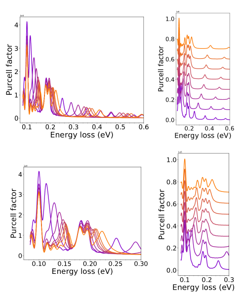
I.6 Purcell factor calculations
In order to understand the experimental measurements more quantitatively, we present numerical simulations of the optical response of our system (Ag nanowires on top of h-BN thin films) carried out by using a finite-difference in the time domain (FDTD) method. In these simulations, plasmon modes are excited by an electric dipole source placed near the end of the nanowire, at a position away from high-symmetry points in order to guarantee a nonzero electric field of the plasmon standing wave, and therefore, a high excitation efficiently. We exploit the proportionality between the EELS probability and the local density of electromagnetic states (LDOS) [1]
| (1) |
where is the elementary charge, is the frequency of the electromagnetic field, , and is the electron velocity. Here, is the projected LDOS (along the direction of the electron trajectory, which is taken along the axis) at the in-plane position of the electron trajectory and evaluated in wave vector space along the direction. Instead of this quantity, we compute the LDOS in real space along , which is in turn proportional to the so-called the Purcell factor (i.e., the enhancement of the decay rate of a dipole emitter placed at the position of interest, compared with the free space decay rate ). More precisely [2],
| (2) |
Although the LDOS forms in two expressions above are not equivalent, we argue that both plasmons and polaritons are extremely localized in space, so the main contribution to EELS will be roughly described by the second form, which is more direct to compute in our method.
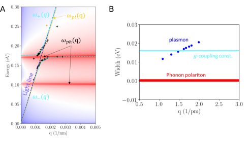
I.7 Strong coupling
Experimental data shows the anti-crossing behavior apparent to the strong coupling regime between plasmon and phonon modes. This can be modeled using a classical model of strongly coupled harmonic oscillators whose dispersion is give by a simple expression
| (3) |
where is the plasmon resonant frequency, is the phonon resonant frequency and is the coupling strength between plasmons and the phonons. The later served as a fitting parameter for us to fit the experimental data using the analytically calculated plasmon dispersion of the infinite nanowire and the phonon dispersion curves for the h-BN thin film. The infinite nanowire plasmon dispersion can be shown to be given with the expressionAshley and Emerson (1974)
| (4) |
where is the wire radius, is the azimuthal order of the plasmon ( in our case), , , and is the transverse wave vector in medium . The phonon-polariton modes of the h-BN film are calculated from Fresnel reflection coefficient. In particular, for Fig. S13A we use the imaginary part of the reflection coefficient for the polarized fields , which readily gives the hyperbolic phonon-polaritonic bands (KF modes). In Fig. S13B we compare the coupling strength with the plasmon and phonon resonance widths that are again extracted from simulations. It is clear that the coupling strength is larger than the plasmon and phonon widths for small values of , therefore indicating that the system undergoes strong coupling
II Supplementary figures