jkrich@uottawa.ca
1Department of Physics, University of Ottawa, ON, Canada
2School of Electrical Engineering and Computer Science, University of Ottawa, ON, Canada
Simudo: a device model for intermediate band materials
Abstract
We describe Simudo, a free Poisson/drift-diffusion steady state device model for semiconductor and intermediate band materials, including self-consistent optical absorption and generation. Simudo is the first freely available device model that can treat intermediate band materials. Simudo uses the finite element method (FEM) to solve the coupled nonlinear partial differential equations in two dimensions, which is different from the standard choice of the finite volume method in essentially all commercial semiconductor device models. We present the continuous equations that Simudo solves, show the FEM formulations we have developed, and demonstrate how they allow robust convergence with double-precision floating point arithmetic. With a benchmark semiconductor pn-junction device, we show that Simudo has a higher rate of convergence than Synopsys Sentaurus, converging to high accuracy with a considerably smaller mesh. Simudo includes many semiconductor phenomena and parameters and is designed for extensibility by the user to include many physical processes.
1 Introduction
Device models are essential components of the development of semiconductor devices, from transistors to solar cells to lasers. Standard semiconductor device models, such as Synopsys Sentaurus, treat materials with 0, 1, or 2 bands (i.e., dielectrics, metals, and semiconductors, respectively) along with an electrostatic potential. At a given location in a given material, each band has its own carrier concentration, with particle motion given by diffusion and electric-field-induced drift. Since the electric field itself depends on particle motion, the resulting Poisson/drift-diffusion (PDD) equations are nonlinear and require numerical solution in the general case Bank1983 ; Fichtner1983a ; Markowich1986 ; Piprek18 ; Schenk1998 .
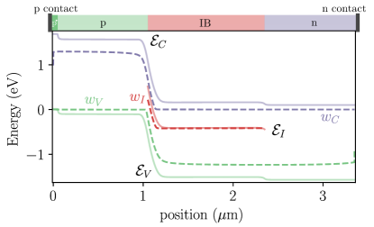
A new class of materials, called intermediate band (IB) materials, has been developed over the last 20 years with the goal of improving solar cell efficiency and producing effective infrared photodetectors Luque97 ; Okada15 ; Mailoa14 ; Berencen17 ; Wang18 . These IB materials are like semiconductors except they have an extra band of allowed electronic energy levels above the valence band (VB) and below the conduction band (CB), as shown in Fig. 1. Such a band structure permits optical absorption from VB to IB and from IB to CB, which is the key to the increased solar cell efficiency Luque97 . It is also possible to consider multiple IBs, though such materials have not yet been realized in practice Brown02 .
Where IB devices have been made, they have not generally been highly efficient, which is believed to be largely due to fast nonradiative recombination processes Okada15 ; Marti06 ; Wang09 ; Lopez11 ; Mailoa14 ; Berencen17 ; Wang18 ; Sullivan15 . It has not been possible, however, to perform standard device modeling to optimize these devices, to determine the ideal layer thicknesses, doping levels, etc., since standard semiconductor device models do not allow the possibility of treating a third band. Therefore, we do not know what efficiencies existing IB materials could permit, if they were optimized. Interpreting experiments on IB materials and designing the best devices require device modeling capabilities.
In order to describe the basic physics of IB devices, one must be able to describe
-
1.
Optical processes between CB, VB, and IB, with rates dependent on IB filling fraction ,
-
2.
Nonradiative processes between CB, VB, and IB, with rates dependent on ,
-
3.
Carrier transport within the IB,
-
4.
Junctions with standard semiconductors.
There is a large array of standard numerical semiconductor device models based on the coupled Poisson and carrier-continuity equations, including general purpose ones, such as Synopsys Sentaurus and Silvaco, as well as more specialized models such as Crosslight, which includes modelling of quantum well physics and a coupled treatment of carrier-density dependent optics for lasers, and TiberCAD Maur08 . Nextnano++ also includes features specific to quantum structures and can solve an 8-band k.p model self-consistently with the Poisson and drift-diffusion calculations Birner2007 . There are also more focused ones, such as PC1D Clugston97 ; Haug16 , AFORS-HETVarache15 , SCAPS Burgelman00 , and Solcore Alonso-Alvarez2018 , which are 1D models focused on solar cells. Many of these models allow treatment of deep-lying states inside the semiconductor band gap, primarily as Shockley-Read-Hall (SRH) trapping and recombination centers Shockley52 . Sentaurus and PC1D, for example, do not permit optical generation from the deep-lying states. SCAPS does permit both thermal and optical processes, but does not consider transport of carriers inside the defect band. We do not attempt a full characterization of all the available device models, but Table 1 shows which of these requirements are met by these device models.
| IB optics with photofilling | IB nonradiative processes | IB transport | Junctions | 2D | |
| Sentaurus | N | Y | limited | Y | Y |
| PC1D Clugston97 | N | Y | N | Y | N |
| SCAPS Burgelman00 | Y | Y | N | Y | N |
| TiberCAD Maur08 | N | Y | Y | Y | Y |
| Martí Marti02 | N | N | Y | N | N |
| Strandberg Strandberg11 | Y | N | Y | N | N |
| Tobias Tobias11 , Yoshida Yoshida12a | Y | N | Y | Y | N |
| Simudo | Y | Y | Y | Y | Y |
There have been a number of device models developed specifically for IB materials, mostly for solar cells, all in steady state. These include traditional Luque97 ; Cuadra04a ; Levy08 ; Hu10 and Boltzmann-approximation Strandberg17 ; Strandberg17a detailed balance models, semianalytic models in the drift Lin09 and diffusion Marti02 ; Navruz08 ; Krich14 limits, and PDD models Yoshida10 ; Strandberg11 ; Tobias11 ; Yoshida12a . The semianalytic models are specific to either the drift or diffusive limits, while the PDD models allow treatment of IB regions that are neither fully depleted nor fully quasi-neutral. A comparison of the features of the PDD models is also included in Table 1. To our knowledge, none has been released as open-source software.
Here we introduce Simudo, a free and open source steady state PDD solver with self-consistent optics for arbitrary numbers of bands. Simudo uses the finite element method (FEM) to solve the coupled Poisson, drift-diffusion, and Beer-Lambert optical propagation equations self-consistently, when necessary including changing according to local generation and recombination, with associated changes in the optical absorption coefficient. Simudo has built-in radiative recombination, Shockley-Read trapping, and SRH recombination models in the non-degenerate limit and is straightforward to extend to include other models of generation or recombination. All of the band parameters, from energies to mobilities to cross sections, can vary in space or as functions of other parameters.
Simudo has a number of innovations in its formulation of the problem, described below, and allows high-accuracy simulation of benchmark semiconductor problems while working with 64-bit arithmetic, making it useful both for standard semiconductor simulations as well as for IB devices. It is written in the Python programming language, using the FEniCS platform to solve the FEM problem AlnaesBlechta2015a . It exposes an easy-to-use API for defining problems and extracting results. It is designed for two-dimensional systems and is available for download at https://github.com/simudo/simudo.
Semiconductor device modeling is typically performed using the finite volume method (FVM), which ensures local charge conservation at each cell in the domain Eymard00 . Finite element methods are less common in semiconductor device models, though there are a number of examples He91 ; Maur08 ; Nachaoui99 ; Bochev15 . FEM is widely used for related advection-diffusion problems in computational fluid dynamics (CFD) studies Cockburn00 . Commercial packages for CFD, as for semiconductor device modeling, are generally based on the FVM method. TiberCAD, a commercial device modeling package with many novel features, uses FEM with continuous basis functionsMaur08 . Finite element methods including discontinuous local basis functions, called discontinuous Galerkin (DG) methods, also permit local charge conservation Cockburn00 , and they have recently begun to be applied to semiconductor device problems Kumar16 ; Kumar17 . FEM methods simplify consideration of complicated simulation domains and in theory allow higher-order convergence of solutions, but performance of such methods can only be determined with testing. We use such a DG-FEM method here to produce a general purpose steady state PDD solver capable of treating IB systems, and we show that Simudo realizes the higher-order convergence with mesh size, converging much more rapidly than Synopsys Sentaurus as the mesh spacing is reduced. As shown in Sec. 3.5, for a reference pn-diode, Simudo demonstrates quartic self-convergence with mesh density while FVM-based Synopsys Sentaurus demonstrates only quadratic convergence. In the reference problem, Simudo achieves 5-6 digits of convergence with 193 mesh points while Sentaurus requires more than 3000. Simudo provides both a flexible framework for the study of IB devices and also a freely available example of a DG-FEM semiconductor device model.
In Section 2, we define the coupled partial differential equations (PDEs) Simudo solves. Section 3 describes the heart of Simudo, giving in detail the conversion of the equations of Section 2 to the weak forms solved using FEM. This section describes the choices for dynamical variables, the weak forms used for FEM, and how these choices enable Simudo to achieve accuracy despite the problems of finite precision arithmetic. This section concludes with a comparison to Synopsys Sentaurus on a benchmark pn-diode, showing the high quality of Simudo’s results. Section 4.1 gives examples of setting up a simple problem using the API, including examples of its convenient topology definitions and Section 4.2 demonstrates the extensibility of Simudo to include new physical processes (in this case, Auger recombination). Section 4.3 demonstrates the use of Simudo to analyze a system originally studied in Ref. Marti02 , showing that its model works better than had been anticipated in the case with equal subgap optical absorption cross sections, but that unequal subgap absorption cross sections produce more complicated phenomena that require IB transport to describe properly.
2 Statement of problem
In this section, we describe the mathematical model of the steady state PDD and optical problems we use in Simudo. Carriers both drift in response to electric fields and diffuse. Carriers are generated optically and recombine using a variety of models. The local carrier concentration determines both the electric field and the optical absorption coefficients, so the transport, Poisson, and optical propagation equations are all coupled. Symbols used in this manuscript are summarized in Table 2.
| Symbol | Definition |
|---|---|
| Carrier density in band | |
| Band edge energy of band ; central energy of IB | |
| Sign of carriers in band (+ for VB, - for CB) | |
| Quasi-Fermi level of carriers in band | |
| Current density in band | |
| Mobility of carriers in band | |
| Diffusion coefficient of carriers in band | |
| Surface recombination velocity of carriers in band | |
| Effective density of states for nondegenerate band | |
| Integrated density of states for intermediate band | |
| Filling fraction of IB | |
| for positive sign and for negative sign | |
| Charge neutral filling fraction of IB | |
| Net generation in band due to all generation and recombination processes | |
| Temperature | |
| Boltzmann constant | |
| Elementary charge | |
| Electrostatic potential, electric field, and charge density | |
| Optical absorption coefficient from band to at vacuum wavelength | |
| Optical cross section from band to | |
| Photon spectral flux density at wavelength lambda in direction | |
| Photon flux in direction from to , i.e., | |
| Surface normal vector | |
| Direction of light propagation |
2.1 Carrier transport and generation
We consider a CB, a VB, and some number of IBs under the assumption that the carrier population in each band is in local quasi-equilibrium with a temperature and quasi-Fermi level , where can be one of for the CB, VB, and IB, respectively. In the case of multiple IBs, can take values , indexing the various IBs, but we simplify the following discussion to consider the case of just one IB, indexed as .
In the most common approximation of semiconductor device modeling, the carrier dynamics in each band can be described by the drift-diffusion equation and the continuity equation. Letting represent the carrier concentration in band , and are the hole and electron concentrations, respectively, which we use interchangeably with their standard symbols, and . We let give the charge of the carriers in band , for the VB and -1 for the CB. Then
| (1a) | ||||
| (1b) | ||||
where is the current density of carriers in band , is the carrier mobility, is the carrier diffusion constant, is the electric field, is the elementary charge, and contains all the generation, trapping, and recombination processes (see Section 2.2). For non-degenerate bands in which is sufficiently far from the band edge , we can write
| (2) |
where is the effective density of states of band , is the electrostatic potential, and is Boltzmann’s constant.
Then, assuming is spatially constant,
| (3) | ||||
| (4) |
For such nondegenerate bands, the Einstein relation gives , from which Eq. 1a gives Fichtner1983a
| (5) |
which we use instead of Eq. 1a. Equation 5 also applies to the case of degenerate bands, as shown in Poupaud1991a , even though the Einstein relation requires a modification. Moreover, Eq. 5 applies in the case of spatially-varying band structure (e.g., spatially-varying )Marshak1984a , so it is considerably more general than this derivation.
Since an intermediate band is often partially filled, we cannot model it using the non-degenerate approximation of Eq. 2. We write for the density of states of the IB, such that is the total density of IB states. If the IB has quasi-Fermi level , the electron concentration is
| (6) |
If the bandwidth of the IB is narrow relative to , we can approximate the IB density of states as a Dirac delta , and so
| (7) |
where is the filling fraction of the IB, and can be written as where is the Fermi function. We work in this limit for the remainder of this manuscript. Extending beyond this sharp-IB case is not difficult but requires more cumbersome notation.
2.2 Carrier generation and recombination
Each band’s continuity equation (Eq. 1b) has a generation term . This term is the sum of contributions from all generation and recombination processes to the band, which depend on which physical models are included in the simulations. We now specify the details of optical generation and a variety of recombination processes , each of which enters either as a negative or positive contribution to , as required for the process.
2.2.1 Optical carrier generation
Modeling optical carrier generation requires modeling the changing light intensity through the device. We use a simple Beer-Lambert model for optical propagation and absorption
| (8) |
where is the photon spectral flux at vacuum wavelength and direction of propagation and is the total absorption coefficient, which can be written as
where is the absorption coefficient for the optical process at wavelength that moves a carrier from band to band . In the usual semiconductor case, and is finite for corresponding to energies larger than the band gap. Free-carrier absorption is included in The carrier generation rate in band due to optical processes is then
| (9) |
Further details of the optical propagation model are described in Section 2.3.
In nondegenerate bands, there are always enough carriers to excite in or out of a band. That is, the valence band always has electrons available, and the conduction band has empty states available to be filled, so the absorption coefficient is insensitive to the free carrier density in the bands. In an IB, however, the VBIB process requires empty states in the IB while the IBCB process requires filled states in the IB. To capture this phenomenon, we write
| (10) | ||||
| (11) |
where is the optical capture cross section from band to at wavelength of a single intermediate state. We can combine these equations into a single expression,
| (12) |
where is just and is the number of holes in band , and is understood to be when . Since depends on the carrier concentrations, and the carrier concentrations depend on (through the generation rate ), the transport and the optical models feed into each other, so they must be solved in a self-consistent manner.
2.2.2 Recombination and trapping
Simudo offers several built-in radiative and nonradiative recombination and trapping mechanisms using the non-degenerate limit for the CB and VB, each including an equivalent thermal generation. An example is the SRH recombination model with a single trap level at energy Shockley52 , in which two trapping processes (of an electron and a hole) produce a recombination event, with recombination rate
| (13) |
where are the carrier lifetimes and are the carrier concentrations of holes and electrons, respectively, if their quasi-Fermi levels were equal to . This appears as a negative contribution to for both CB and VB.
We can model traps as intermediate bands with tracked explicitly, in which case we implement standard Shockley-Read trapping Shockley52 ,
| (14) |
where is the IB filling fraction of carriers with charge , and is the Shockley-Read lifetime for band , as in Eq. 13 Shockley52 . Note that makes a negative contribution to and a positive contribution to , while makes a negative contribution to both and .
Simudo also implements radiative trapping from band to . When we use Boltzmann statistics rather than Bose statistics for the emitted photons, which is valid when remains at least a few below , as in Ref. Strandberg11 , then the radiative trapping can be written
| (15) |
where
| (16) |
where is the index of refraction, and is either or for , respectively. Note that Ref. Strandberg11 includes only the recombination term, and we add the corresponding thermal generation term, which is the -1 in Eq. 15. We can re-express Eq. 15 in a similar form to the nonradiative terms by using the relation
As with Eq. 2, Eqs. 14-16 are valid in the non-degenerate limit where does not approach but full degenerate statistics are used for the IB. Extensions to the degenerate limit can be added, if desired. Simudo also treats standard radiative recombination between conduction and valence bands Nelson03 .
We also treat surface recombination at external surfaces of the device, which imposes a boundary condition
| (18) |
where is the surface recombination velocity of carriers in band at boundary is the normal to , and is the carrier concentration at equilibrium McIntosh14 . The current release of Simudo supports only or , which impose or , respectively.
2.3 Optical equations
For each wavelength, we need to solve the optical propagation according to Eq. 8. For stability of the numerical solution, it is convenient to use a second-order equation so that we can apply boundary conditions on both the inlet and outlet boundaries Zhao2013a . We take the derivative of Eq. 8 with respect to the direction of propagation,
| (19) |
With no reflection from the back, the boundary conditions are then
| (inlet) | (20a) | |||||||
| (outlet) | (20b) | |||||||
where is a spectral photon flux at the inlet boundary.
In the case where is constant for in an interval , the optical flux at all wavelengths in that range obeys Eq. 19 and can thus be treated together. We can write
where is a photon flux (where is a spectral photon flux). In this case, we have
Simudo uses this form, which allows simple treatment of piecewise constant absorption coefficients with a small number of optical fields . When optical fields with only one propagation direction are considered, we write the spectral flux density and the flux density .
2.4 Poisson’s equation
In electrostatics, Poisson’s equation relates , the charge density , and the permittivity ,
| (21) |
It can also be split into two equations
| (22a) | ||||
| (22b) | ||||
where is the electric field.
The charge density is the sum of the static charge and the mobile charge in each band. In an IB material,
| (23) |
where , are the shallow acceptor and donor doping concentrations, respectively, the mobile charge in the IB is , with the IB filling fraction of the bulk IB material at . For a donor-type IB , and for an acceptor-type IB . Note that in writing the shallow dopant terms and , we are assuming complete ionization of these impurities.
3 Numerical method
Simudo uses the finite element method (FEM) to solve the coupled Poisson/drift-diffusion and optics problems, given by Eqs. 1b,5,19, and 22. The FEM method divides the simulation domain into cells, which are generally triangles in 2D, and enforces a weak form of the desired PDE’s with a set of test functions defined on those cells, with boundary conditions applied on the domain boundary . The method is well-described in many reference texts Johnson1987a ; Gockenbach2006a ; Donea2003a . In this section, we detail the weak forms used for these coupled equations and the solution method for the resulting nonlinear system. We benchmark Simudo against the industry standard Synopsys Sentaurus commercial simulator on a standard semiconductor problem to show the quality of our results.
3.1 Solution method
The PDD problem is a coupled nonlinear system of PDEs, which we solve iteratively using Newton’s method as implemented in the FEniCS package. The solution procedure is outlined in Fig. 2. The goal is to find a solution that satisfies Eqs. 1b,5,22 and associated that obeys Eq. 19. The optical problem is solved alongside the PDD problem in a self-consistent manner. That is, the PDD subproblem produces the absorption coefficient (which, for processes involving the IB, depends on the filling fraction). The optical subproblem is then solved using these absorption coefficients, yielding a new photon flux , which is fed back into the PDD where it enters in the optical carrier generation process, and the cycle iterates until a self-consistent solution is found.
The convergence of Newton’s method depends on the quality of the initial guess. Steps 1 and 2 in Fig. 2 are the pre-solver, which is used once to make the initial guess for the main Newton solver, illustrated in step 3. The full procedure is:
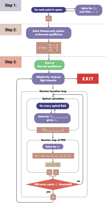
-
1.
For each point in space, calculate the equilibrium Fermi level at that point assuming local charge neutrality and .
Physically, this step finds the in each location that makes it charge neutral, before any charge is allowed to flow.
-
2.
Determine the built-in potential of the equilibrium system, using as the initial guess. That is, solve only Eq. 22 for while keeping all and thus all .
Physically, this step allows charge to move, forming depletion regions as the carriers move to achieve a zero-current configuration that satisfies Poisson’s equation. The carrier density inside bulk-like regions of space changes little from the bulk equilibrium value in step 1, making an excellent guess in large regions of space.
-
3.
Main solver loop Adaptively ramp up light intensity and/or bias, starting with thermal equilibrium (dark, no bias). Each solution requires a loop of Newton iterations. Within each Newton iteration, do the following:
-
(a)
Optical calculation For each optical field , solve for the photon flux given the latest value of . Note that Eq. 19 is linear when is fixed.
-
(b)
PDD Newton step Perform one Newton step of the PDD problem.
-
i.
Solve for . Use the value of (and thus optical carrier generation) computed in the previous step.
-
ii.
Update .
As an option, logarithmic damping can be applied to to prevent Newton’s method from diverging, e.g., where for or other user-defined value Gaury2019a .
-
i.
-
(a)
We now describe the weak forms that we use for each of Eqs. 1b,5, 19, and 21. There is much flexibility in the choice of particular weak forms, all of which can be equivalent to the same strong form. In Section 3.3.2 we illustrate the use of a partitioned offset representation for , which allows internal currents to be calculated accurately with double-precision arithmetic.
3.2 Poisson equation
Here we introduce the formulation we use to implement Eq. 22. We use a mixed method to solve for both and explicitly Brezzi1985a ; Roberts1991a . The potential is represented as a superposition of discontinuous Galerkin (DG) basis functions of order (cell-wise discontinuous polynomials), and is represented using Brezzi-Douglas-Marini basis functions of order (cellwise discontinuous polynomials with continuous normal component on cell boundaries) Brezzi1985a . We use the BDM space for all vector quantities, including and . The BDM space is H(div) conforming, meaning the divergence is accurately calculated and fluxes between cells are preserved, which makes it a natural choice for conserved or almost conserved vector quantities.111In the BDM space, the normal fluxes are shared by adjacent elements. The flux exiting the perimeter of a collection of cells exactly equals the sum of fluxes out of each of the cells, with exact arithmetic. While is not a conserved quantity, due to generation and recombination that occur inside of cells, the BDM space ensures that is accurately preserved when passing between cells. A method using CG or DG functions for would be susceptible to numerical errors associated with non-conservation of currents between cells, and we show in Sec. 3.3.2 that Simudo conserves current well in a pn diode. In the results below, .
We multiply Eq. 22a by test function and Eq. 22b by test function , then integrate each spatially, giving the weak forms
| (24) | ||||
| (25) |
which must hold for every test function and , where is the full domain and is the boundary. Note that Eq. 24 includes an integration by parts. In this case, the electric field BC is an essential BC, imposed by reducing the set of test functions to those that satisfy the BC, while the potential BC is a natural BC.
3.3 Transport equations
The drift-diffusion equations are often numerically challenging to solve in semiconductors. In carrier density-based formulations, poor resolution of the gradients of makes linear interpolation of current density unstable, which the Scharfetter-Gummel box method corrects for FVM methods Bank1983 . Additionally, catastrophic cancellation can occur in Eq. 1a, e.g., for the majority carrier in a quasi-neutral region of a semiconductor, when the drift and diffusion contributions are nearly equal in magnitude. The current is given by the difference and can be hard to evaluate with finite precision arithmetic. We address these issues by using a quasi-Fermi-level-based representation for carrier density Cummings09 ; Nachaoui99 . Calculating in finite precision for Eq. 5 can also be challenging when is very flat, and in Sec. 3.3.2 we introduce a partitioned offset representation for to allow accurate determination of with essentially no extra computational cost. We use a mixed FEM method that solves explicitly for both and the current density . As described in Sec. 3.2, the BDM space of basis functions enforces local current conservation in the solutions, which also enables local current densities to be well determined. Without the mixed method, local current conservation is enforced indirectly, and we were not able to obtain well-converged results for local currents.
3.3.1 Quasi-Fermi level formulation
The quasi-Fermi level is represented as a superposition of DG basis functions of order , and the current density is represented using BDM basis functions of order . Section 3.2 contains a discussion of these functions’ properties and of the mixed method. In the results below, .
3.3.2 Quasi-Fermi level offset partitioning
As written, Eq. 26b still suffers from a form of catastrophic cancellation in its last term, which corresponds to the gradient term in Eq. 5. Since for , the last term is nonzero only if varies within the domain where is nonzero. can be extremely flat, for example in quasineutral regions, which makes this integral hard to calculate with finite arithmetic precision. This difficulty is more apparent in Eq. 5: if is small,222relative to a representation of that stores its value on the nodes of the mesh cannot resolve such small changes in across space.
We circumvent this issue by using an offset representation for . The idea is to give each cell in the domain its own (spatially constant) base quasi-Fermi level relative to which the new dynamical variable is expressed. That is, where is the quantity we actually solve for instead of . Before every Newton iteration step, the of each cell is initialized to the cell average of from the previous iteration. This representation allows small spatial changes of to be accurately represented, enabling accurate determination of the current.
The last remaining question is how to adjoin regions with different base values. We connect them by adding a surface integral jump term to Eq. 26b, resulting in
| (27) |
where is the jump operator, which takes the difference between the values of a discontinuous expression on either side of a facet. The rest of this section is dedicated to deriving that term and comparing the result to a formulation without the offset representation.
We substitute into Eq. 26b, and we obtain
| (28) |
Our goal now is to rewrite the term. Since is constant on each cell , within each cell. We integrate by parts using
| (29) |
yielding
| (30) |
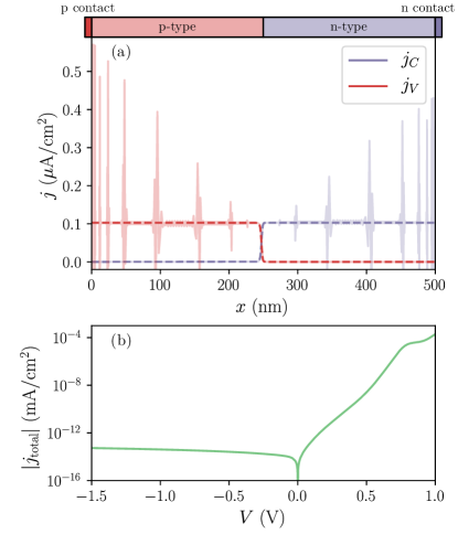
We perform a test of Simudo, which uses the partitioned offset representation, against the identical model without the offset representation. We consider a standard silicon pn-junction diode with symmetric doping of cm-3 and SRH lifetimes of 1 ns and 1 s in the p- and n-type regions, respectively. Each region has a length of 250 nm, for total device length of 500 nm. Although the problem is one-dimensional, we consider a 2D region with a height of . At each contact, the majority carrier has an infinite surface recombination velocity while the minority carrier has zero surface recombination. We use a mesh with 769 points in the x-direction, which is tightest near the contacts and junction and expands out geometrically toward the middle of the quasi-neutral regions. The mesh has 2 points in y-direction, and further details of the mesh are given in Sec. 3.5.
The offset representation allows internal current densities to be resolved accurately throughout the device. Figure 3(a) shows the electron and hole currents under 0.16 V bias. Without the offset representation, the majority currents are poorly resolved, due to the inability to resolve with double-precision arithmetic. The majority currents in the no-offset model become worse as the mesh density increases (not shown), as expected for approximations of . Figure 3(b) shows the total charge current density at the contact, and the results with and without the offset representation agree to 5 digits. We conclude that the offset representation allows robust extraction of internal current densities but does not seem to be important for the overall current density of the test device. The offset representation imposes essentially no extra computational cost on Simudo while enabling robust determination of internal current densities.
3.4 Optics
The optical problem is solved by self-consistently iterating through the optical flux variables and independently solving Eq. 19 for each one. For convenience, we write , , and for the remainder of this section. We represent using CG basis functions of order .
We now derive the weak form used in Simudo to solve each optical propagation problem. We follow closely the derivation in Zhao2013a of the modified second order radiative transfer equation (MSORTE) method, without the scattering matrix. Integrating Eq. 19 with a test function gives
| (31) |
where and . Using Eq. 29, we obtain
| (32) |
Inserting the outlet boundary condition Eq. 20b into the first term, we obtain the final weak form
| (33) |
The inlet boundary condition Eq. 20a is applied directly on as an essential boundary condition.
3.5 Sentaurus benchmark comparison
To validate Simudo, we benchmark it against the industry standard Synopsys Sentaurus device simulator. Since Sentaurus does not support intermediate band materials, the benchmark is limited to standard semiconductors. Our test problem is the same silicon pn-junction as considered in Section 3.3.2, with the overall as shown in Fig. 3(b). See below for a discussion of the differences in implementation of the Ohmic condition between Simudo and Sentaurus.
We study the convergence of the results as the mesh is refined, using a number of mesh points in the x-direction ranging from 45 to 12289, with the same meshes used for both Sentaurus and Simudo. The mesh spacing is nonuniform in the x-direction since the carrier and current densities vary most rapidly near the contacts and the junction. The meshes are generated by splitting the structure into two regions, one extending from the p-contact to the junction and one from the n-contact to the junction. In each region, a mesh spacing is applied to the cell adjacent to the contact and the cell adjacent to the junction. The mesh spacing increases geometrically toward the center of each region with a growth factor of 1.2. To generate the finest mesh sizes, these cells are further subdivided into 4, 16 or 64 equal parts. There are 2 points in the y-direction. The computational cost generally increases with the number of degrees of freedom rather than with the number of cells in the mesh. Simudo has more degrees of freedom associated with each cell than Sentaurus, due to its higher-order basis functions. For this mesh, Simudo has 36 degrees of freedom per triangle while Sentaurus has 9 per triangle, with 2 triangles per mesh point. In this mesh, each triangle has at least one edge on the boundary of the device, which increases the number of degrees of freedom per triangle compared to a mesh where most triangles share sides; this effect is similar for both methods.
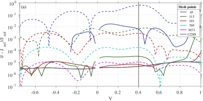
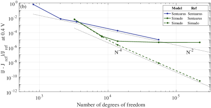
Figure 4(a) shows the results of the study, where we plot the relative error in for each simulation, with the reference current taken from Sentaturus with the densest mesh. With 193 mesh points, Simudo converges approximately as well as Sentaurus with 3073 mesh points. Above 769 mesh points, the Simudo results show no further improvement in error, indicating either that Simudo and Sentaurus converge to results that differ at the level or that Sentaurus with 12289 mesh points is only converged to the level, while Simudo may have converged more precisely. The simulations were performed on different machines, so we do not report timing data.
The figure makes clear that Simudo converges much more rapidly with mesh size than Sentaurus, which demonstrates the higher order convergence that FEM is supposed to provide over FVM. Figure 4(b) shows the scaling of the errors with the number of degrees of freedom in each simulation, at 0.4 V. The solid blue line shows that Sentaurus’ self-convergence scales like with the number of degrees of freedom. The dashed green line shows Simudo’s self-convergence, with taken from the Simudo simulation with 12289 mesh points. It shows that Simudo’s self-convergence scales like with the number of degrees of freedom. For all but the smallest meshes, Simudo’s convergence is superior to Sentaurus’ at the same number of degrees of freedom. Taken together, these figures show that with 193 mesh points, Simudo’s result is as good as Sentaurus’ with 64 times as many mesh points, which is equivalent to 16 times as many degrees of freedom.
Note that the boundary conditions at the contacts are not precisely the same for the Sentaurus and Simudo simulations. Both are intended to simulate Ohmic contacts for the majority carrier and surface recombination velocities of 0 for the minority carrier. The Simudo simulations are performed with surface recombination velocity and 0 for the majority and minority carriers, respectively, imposing equilibrium carrier concentration at the boundary for majority carriers and setting for minority carriers, as described in Sec. 2.2.2. The Sentaurus simulations are performed with for the minority carriers, in agreement with Simudo, and the default “Ohmic contact” boundary condition for the majority carriers, which imposes charge neutrality and equilibrium carrier concentration at the contact. Under small and reverse bias, these two sets of boundary conditions should be equivalent, but under large forward bias, the default Sentaurus boundary condition is expected to give incorrect results due to its imposition of charge neutrality Synopsys15 . Sentaurus provides a “Modified Ohmic” boundary condition, which should be closer to the Simudo boundary condition, but we were unable to attain convergence using it. As a result, at larger biases the Simudo and Sentaurus results diverge from each other, and we do not include them in Fig. 4. For biases larger than 1 V, the diode is in high injection, and the Boltzmann approximation used in this calculation is not accurate, regardless.
4 Examples and results
In this section, we give examples of using Simudo. Section 4.1 shows how to set up a simple 1-dimensional pn-junction device and demonstrates the helpful tools that Simudo provides for defining regions and boundaries. Section 4.2 shows the extensibility of Simudo by illustrating the code required to add a new Auger recombination process. Section 4.3 illustrates the use of Simudo to study a system first considered in Ref. Marti02 .
4.1 PN junction and topology definitions
We include in the supplementary material the code listing equilibrium.py describing a simple pn-junction device in Simudo. This example constructs the device and implements steps 1-4 of the pre-solver shown in Fig. 2. Here, we discuss some of the pieces of that code and illustrate the useful topology construction operations built in to Simudo.
In the 1-dimensional pn-junction example, the object ls contains information about the layers, including their sizes, positions, and mesh. The object pdd sets up the Poisson/drift-diffusion solver and has information about the bands in each material, including recombination processes and boundary conditions. In this example, there are only two bands (VB, CB); for a problem including an IB, pdd would have a third band, too.
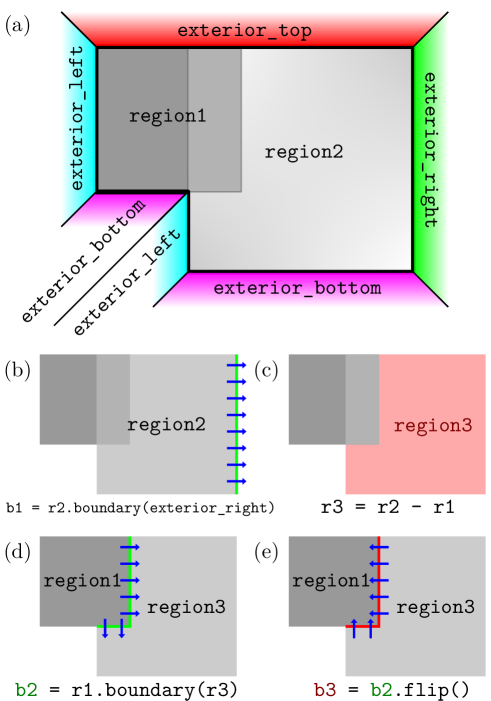
Simudo is designed for 2-dimensional simulations, and it has sophisticated tools to define the arrangement of materials, dopings, contacts, meshing regions, or other user-defined spatial properties. In many FEM solvers, interfaces must be tracked manually, including their orientation, to ensure that integrals over those interfaces are added together properly. Simudo introduces a set of topology tools that instead allow users to define the regions and interfaces in which they are interested, and Simudo takes care of all the bookkeeping. The user defines regions as desired (e.g., emitter, base, defective-region), which can then be given properties, whether they be doping levels, recombination parameters, or other desired properties. These regions are initially defined abstractly, without having any coordinates in the device, using CellRegions and FacetRegions, and are later connected to geometry and materials by the mesh generator.
Full details are given in the documentation accompanying Simudo, but
we give a further illustration of these methods in Figs. 5
and 6. That example illustrates the
creation of arbitrary CellRegion objects, including unions
and intersections, and edges that connect them. When R
is a CellRegions container, accessing a nonexistent attribute
(such as R.domain) causes its creation. The user can define
new CellRegion objects by applying Boolean operations
on previous ones and new FacetRegion objects by using
the boundary method. For example, consider the region
R.region1. Then
R.region1.boundary(R.region2) creates a signed boundary
from region1 to region2, as illustrated in
Fig. 5. All of these custom regions are
kept as symbolic expressions and evaluated by Simudo only when needed
(e.g., when asked to apply a boundary condition or when asked to compute
a volume or surface integral). This layer of abstraction allows the
user not to worry about the details of mesh markers, entity indices,
and facet orientations LoggMardalEtAl2012a , and is described
more fully in the documentation that accompanies Simudo.
The examples in Figs. 5-6 illustrate another useful concept. The mesh generation interprets the external region as being outside the simulation domain, allowing convenient definitions for boundary conditions and current flow. The FacetRegions are used in the pn-junction example shown in the supplementary material to define the boundary conditions, which – in step 2 – are conductive at the left and right contacts and nonconductive at the top and bottom surfaces. That example also shows how the mesh can be refined by adding extra mesh points near the contacts.
4.2 Extensibility: Adding Auger recombination
The initial release of Simudo contains radiative and Shockley-Read trapping and recombination processes in the non-degenerate limits for VB, CB. The user can easily add modified physics to their problems, which we demonstrate here with an example of adding an Auger recombination process to Simudo, with the form
| (34) |
where are the Auger coefficients, and and are the hole and electron concentrations at thermal equilibrium, respectively Nelson03 . The code is listed in Fig. 7. The function get_generation_user(band) adds a negative local generation rate in the CB and VB and returns 0 for all other bands. This recombination process moves particles between two bands, the src_band and the dst_band. In this case, where the electrons and holes have opposite charge, the Auger process destroys both particles simultaneously; if both carrier types involved in the process had the same charge (e.g., for a CB-to-IB trapping process), the process would represent a particle-number-conserving transfer (rather than a recombination) from the src_band to the dst_band, with the appropriate sign for the recombination process determined by the get_band_generation_sign method (inherited from TwoBandEOPMixin). This method’s sign convention is that the dst_band always gains carriers through the generation process, while the src_band gains or loses as required by conservation of charge.
4.3 P[IB]N junction
In Ref. Marti2002a , the authors consider a quantum-dot-based IB solar cell with a p-n-IB-p-n structure. They present a drift-diffusion model for the IB region only, with the carrier density and current density boundary conditions obtained from a depletion approximation and law of the junction. This model assumes that transport is diffusion-dominated in the IB region, and drift can therefore be neglected. This early device model gave important insights into the behavior of IB devices.
| Value | Definition |
|---|---|
| Conduction band edge energy | |
| Intermediate band energy | |
| Valence band edge energy | |
| CB and VB effective density of states | |
| IB density of states | |
| CB and VB mobility | |
| IB mobility | |
| Absorption coefficient for CV process | |
| Optical cross section for CI process | |
| Optical cross section for IV process | |
| Dielectric constant | |
| Sun temperature | |
| Cell temperature | |
| Solar concentration factor | |
| IB region length | |
| Charge-neutral IB filling fraction |
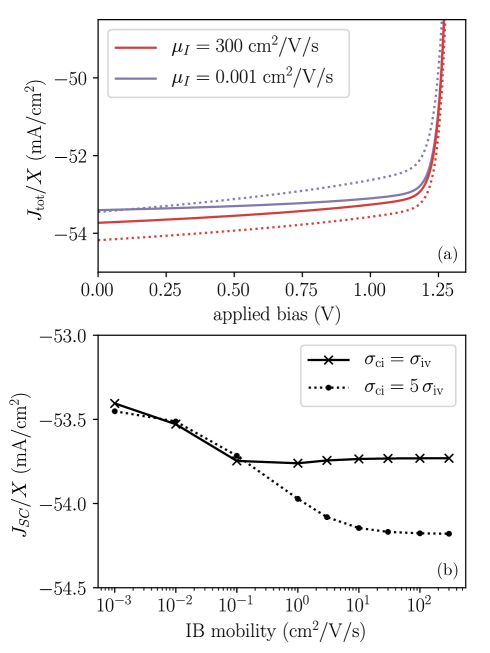
In testing the self-consistency of the model, the authors estimate the IB mobility required to remain in the diffusion-dominated regime, finding that an IB mobility greater than is required to make their model consistent. This claim raises an immediate question: does something interesting happen when the IB mobility goes below that threshold? Since Simudo is a full drift-diffusion device model, we can directly answer that question.
We model a similar device with a simpler p-IB-n structure. This device has the same band and absorption parameters as the device described in Marti2002a , summarized in Table 3. The incident light is a blackbody spectrum at with a solar concentration factor . The device has equal subgap optical cross sections and nearly current matched (within 10%) incident photon fluxes for the two subgap transitions. In this case, the local IV and CI generation rates are nearly identical throughout the IB device. The code to set up this problem is included in the supplementary material, in marti2002.py.
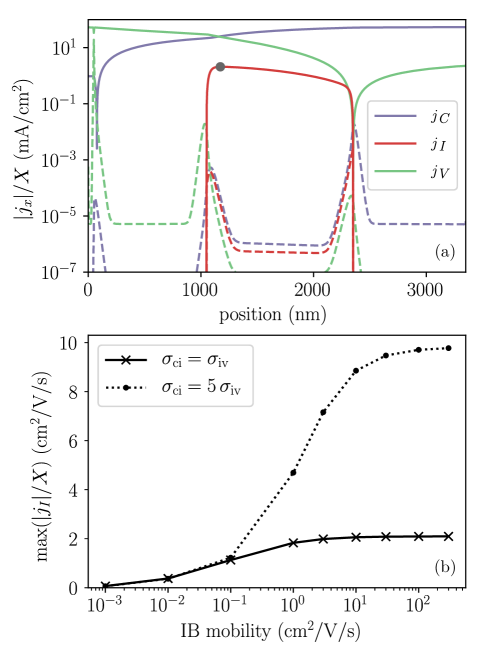
We simulate this device with ranging from to , with resulting J-V curves shown as solid lines in Fig. 8a, which is tightly zoomed and still shows only minor effects of this over- change in . In fact, the IB and drifts currents contribute negligibly to the transport inside the IB region and the current remains diffusion-dominated throughout, as shown in Fig. 9a.
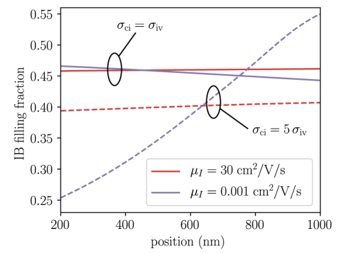
The device behavior is approximately independent of because the IV and CI generation rates are roughly equal at each point in the device, so IB transport is not required to enable sub-gap current matching, but this behavior is not generic for all IB devices. We illustrate this effect by increasing by a factor of five (while keeping unchanged). In this case, the device is still globally approximately current-matched, but the CI absorption process occurs preferentially at the top of the device while the IV generation occurs deeper in the IB region. The device thus relies on IB transport for the CI and IV generation rates to balance over the full device. These effects are shown in the dashed curves of Fig. 8, which show a stronger dependence on than in the matched case. When IB mobility is low, the excess CI generation in the front of the device instead causes local CI trapping, with equivalent local IV trapping toward the back of the device, reducing overall current. In the high-mobility case, the overall current is slightly larger with the mismatched absorptions, due to the increased optical depth. Figure 8b shows how varies with in both of these cases, where the greater dependence on in the mismatched case is apparent. Figure 9b shows that in the matched- case, is never particularly large, while it grows to be five times larger in the mismatched case, showing the role of IB currents in internally balancing the optical absorptions.
In the low-mobility limit, where is always small, when local CI and IV current generations are imbalanced, the filling fraction of the IB must shift to equalize generation and recombination at each point Strandberg09 . This effect is visible in Fig. 10, where at low mobility, the mismatched- case has photodepletion at the front side and photofilling at the back side, consistent with excess CI generation at the front and excess IV generation at the back. Both the matched- and the high-mobility mismatched- cases maintain an approximately uniform IB filling fraction.
These examples together show the utility of Simudo to explore the performance of IB devices and resolve an assertion made in earlier device models without the benefit of a coupled PDD/optics solver.
5 Conclusion
The availability of a device model for intermediate band materials should enable both understanding of this new class of materials and optimization of IB devices. Simudo’s use of the FEM and its methods for overcoming catastrophic cancellation may also prove useful in standard semiconductor device simulation. Simudo has been validated against Synopsys Sentaurus for standard semiconductor devices and shown to converge more rapidly with mesh size. This self-consistent solution of the Poisson/drift-diffusion and optical propagation equations provides a platform for studying a wide range of optoelectronic materials and devices, including solar cells and photodetectors, with tools to enable extensibility to arbitrary generation and recombination models, thermal effects, and more. The near-term roadmap for Simudo includes explicit heterojunction support and nonlocal tunneling, which will be available with future releases at github.com/simudo/simudo. We hope that the free and open source nature of this software will enable further development of IB materials and device simulation more broadly.
Acknowledgments
We acknowledge funding from US Army Research Laboratory (W911NF-16-2-0167), the Natural Sciences and Engineering Research Council of Canada TOP-SET training program, and computing resources from Compute Canada. We thank Emily Zinnia Zhang for alpha testing Simudo, contributing the first code implementing trapping processes, and valuable conversations.
References
- (1) R.E. Bank, D.J. Rose, W. Fichtner, Numerical Methods for Semiconductor Device Simulation, IEEE Transactions on Electron Devices 30(9), 1031 (1983)
- (2) W. Fichtner, D. Rose, R. Bank, Semiconductor device simulation, IEEE Transactions on Electron Devices 30(9), 1018 (1983)
- (3) P.A. Markowich, The Stationary Semiconductor Device Equations. Computational Microelectronics (Springer Vienna, Vienna, 1986)
- (4) J. Piprek (ed.), Handbook of Optoelectronic Device Modeling & Simulation (CRC Press, Boca Raton, FL, 2018)
- (5) A. Schenk, Advanced Physical Models for Silicon Device Simulation (Springer-Verlag Wien, 1998)
- (6) A. Luque, A. Martí, Increasing the Efficiency of Ideal Solar Cells by Photon Induced Transitions at Intermediate Levels, Phys. Rev. Lett. 78(26), 5014 (1997)
- (7) Y. Okada, N.J. Ekins-Daukes, T. Kita, R. Tamaki, M. Yoshida, A. Pusch, O. Hess, C.C. Phillips, D.J. Farrell, K. Yoshida, N. Ahsan, Y. Shoji, T. Sogabe, J.F. Guillemoles, Intermediate band solar cells: Recent progress and future directions, Applied Physics Reviews 2(2), 021302 (2015)
- (8) J.P. Mailoa, A.J. Akey, C.B. Simmons, D. Hutchinson, J. Mathews, J.T. Sullivan, D. Recht, M.T. Winkler, J.S. Williams, J.M. Warrender, P.D. Persans, M.J. Aziz, T. Buonassisi, Room-temperature sub-band gap optoelectronic response of hyperdoped silicon, Nat Commun 5, 3011 (2014)
- (9) Y. Berencén, S. Prucnal, F. Liu, I. Skorupa, R. Hübner, L. Rebohle, S. Zhou, H. Schneider, M. Helm, W. Skorupa, Room-temperature short-wavelength infrared Si photodetector, Scientific Reports 7, 43688 (2017)
- (10) M. Wang, Y. Berencén, E. García-Hemme, S. Prucnal, R. Hübner, Y. Yuan, C. Xu, L. Rebohle, R. Böttger, R. Heller, H. Schneider, W. Skorupa, M. Helm, S. Zhou, Extended Infrared Photoresponse in -Hyperdoped at Room Temperature, Phys. Rev. Applied 10(2), 024054 (2018)
- (11) A.S. Brown, M.A. Green, Impurity photovoltaic effect: Fundamental energy conversion efficiency limits, J. Appl. Phys. 92(3), 1329 (2002)
- (12) A. Martí, E. Antolín, C.R. Stanley, C.D. Farmer, N. López, P. Díaz, E. Cánovas, P.G. Linares, A. Luque, Production of Photocurrent due to Intermediate-to-Conduction-Band Transitions: A Demonstration of a Key Operating Principle of the Intermediate-Band Solar Cell, Phys. Rev. Lett. 97(24), 247701 (2006)
- (13) W. Wang, A.S. Lin, J.D. Phillips, Intermediate-band photovoltaic solar cell based on ZnTe:O, Appl. Phys. Lett. 95(1), 011103 (2009)
- (14) N. López, L.A. Reichertz, K.M. Yu, K. Campman, W. Walukiewicz, Engineering the Electronic Band Structure for Multiband Solar Cells, Phys. Rev. Lett. 106(2), 028701 (2011)
- (15) J.T. Sullivan, C.B. Simmons, T. Buonassisi, J.J. Krich, Targeted Search for Effective Intermediate Band Solar Cell Materials, IEEE Journal of Photovoltaics 5(1), 212 (2015)
- (16) M.A. der Maur, A multiscale simulation environment for electronic and optoelectronic devices. Ph.D. thesis, Universita’ degli Studi di Roma Tor Vergata (2008)
- (17) S. Birner, T. Zibold, T. Andlauer, T. Kubis, M. Sabathil, A. Trellakis, P. Vogl, nextnano: General Purpose 3-D Simulations, IEEE Transactions on Electron Devices 54(9), 2137 (2007)
- (18) D.A. Clugston, P.A. Basore, PC1D version 5: 32-bit solar cell modeling on personal computers, in Twenty Sixth IEEE Photovoltaic Specialists Conference (1997), pp. 207–210
- (19) H. Haug, J. Greulich, PC1Dmod 6.2 - Improved Simulation of c-Si Devices with Updates on Device Physics and User Interface, Energy Procedia 92(1876), 60 (2016)
- (20) R. Varache, C. Leendertz, M. Gueunier-Farret, J. Haschke, D. Muñoz, L. Korte, Investigation of selective junctions using a newly developed tunnel current model for solar cell applications, Solar Energy Materials and Solar Cells 141, 14 (2015)
- (21) M. Burgelman, P. Nollet, S. Degrave, Modelling polycrystalline semiconductor solar cells, Thin Solid Films 361-362, 527 (2000)
- (22) D. Alonso-Álvarez, T. Wilson, P. Pearce, M. Führer, D. Farrell, N. Ekins-Daukes, Solcore: a multi-scale, Python-based library for modelling solar cells and semiconductor materials, Journal of Computational Electronics 17(3), 1099 (2018)
- (23) W. Shockley, W.T. Read, Statistics of the Recombinations of Holes and Electrons, Phys. Rev. 87(5), 835 (1952)
- (24) A. Marti, L. Cuadra, A. Luque, Quasi-drift diffusion model for the quantum dot intermediate band solar cell, IEEE Transactions on Electron Devices 49(9), 1632 (2002)
- (25) R. Strandberg, T.W. Reenaas, Drift-diffusion model for intermediate band solar cells including photofilling effects, Prog. Photovolt: Res. Appl. 19(1), 21 (2011)
- (26) I. Tobías, A. Luque, A. Martí, Numerical modeling of intermediate band solar cells, Semiconductor Science and Technology 26(1), 014031 (2011)
- (27) K. Yoshida, Y. Okada, N. Sano, Device simulation of intermediate band solar cells: Effects of doping and concentration, Journal of Applied Physics 112(8), (2012)
- (28) L. Cuadra, A. Martí, A. Luque, Influence of the overlap between the absorption coefficients on the efficiency of the intermediate band solar cell, IEEE Transactions on Electron Devices 51(6), 1002 (2004)
- (29) M.Y. Levy, C. Honsberg, Intraband absorption in solar cells with an intermediate band, Journal of Applied Physics 104(11), 113103 (2008)
- (30) W.G. Hu, T. Inoue, O. Kojima, T. Kita, Effects of absorption coefficients and intermediate-band filling in InAs/GaAs quantum dot solar cells, Appl. Phys. Lett. 97(19), 193106 (2010)
- (31) R. Strandberg, Analytic -Characteristics of Ideal Intermediate Band Solar Cells and Solar Cells With Up and Downconverters, IEEE Transactions on Electron Devices 64(5), 2275 (2017)
- (32) R. Strandberg, The -Characteristic of Intermediate Band Solar Cells With Overlapping Absorption Coefficients, IEEE Transactions on Electron Devices 64(12), 5027 (2017)
- (33) A.S. Lin, W. Wang, J.D. Phillips, Model for intermediate band solar cells incorporating carrier transport and recombination, Journal of Applied Physics 105(6), 064512 (2009)
- (34) T. Navruz, M. Saritas, Efficiency variation of the intermediate band solar cell due to the overlap between absorption coefficients, Solar Energy Materials and Solar Cells 92(3), 273 (2008)
- (35) J.J. Krich, A.H. Trojnar, L. Feng, K. Hinzer, A.W. Walker, Modeling intermediate band solar cells: a roadmap to high efficiency, in Proc. SPIE 8981, Physics, Simulation, and Photonic Engineering of Photovoltaic Devices III (2014), p. 89810O
- (36) K. Yoshida, Y. Okada, N. Sano, Self-consistent simulation of intermediate band solar cells: Effect of occupation rates on device characteristics, Applied Physics Letters 97(13), 133503 (2010)
- (37) M.S. Alnæs, J. Blechta, J. Hake, A. Johansson, B. Kehlet, A. Logg, C. Richardson, J. Ring, M.E. Rognes, G.N. Wells, The FEniCS Project Version 1.5, Archive of Numerical Software 3(100) (2015)
- (38) R. Eymard, T. Gallouët, R. Herbin, in Handbook of Numerical Analysis, vol. 7 (Elsevier, 2000), pp. 713–1018
- (39) Y. He, G. Cao, A generalized Scharfetter-Gummel method to eliminate crosswind effects (semiconduction device modeling), IEEE Transactions on Computer-Aided Design of Integrated Circuits and Systems 10(12), 1579 (1991)
- (40) A. Nachaoui, Iterative solution of the drift-diffusion equations, Numerical Algorithms 21, 323 (1999)
- (41) P. Bochev, K. Peterson, M. Perego, A multiscale control volume finite element method for advection-diffusion equations, Int. J. Numer. Meth. Fluids 77(11), 641 (2015)
- (42) B. Cockburn, G.E. Karniadakis, C.W. Shu (eds.). Discontinuous Galerkin Methods: Theory, Computation, and Applications, Lecture Notes in Computational Science and Engineering, vol. 11 (Springer, Berlin, Heidelberg, 2000)
- (43) G. Kumar, M. Singh, A. Bulusu, G. Trivedi, A Framework to Simulate Semiconductor Devices Using Parallel Computer Architecture, in Journal of Physics: Conference Series, vol. 759 (IOP Publishing, 2016), vol. 759, pp. 012,098–
- (44) G. Kumar, M. Singh, A. Ray, G. Trivedi, An FEM based framework to simulate semiconductor devices using streamline upwind Petrov-Galerkin stabilization technique, in 2017 27th International Conference Radioelektronika (2017), pp. 1–5
- (45) F. Poupaud, C. Schmeiser, Charge transport in semiconductors with degeneracy effects, Mathematical methods in the applied sciences 14(5), 301 (1991)
- (46) A.H. Marshak, C. Van Vliet, Electrical current and carrier density in degenerate materials with nonuniform band structure, Proceedings of the IEEE 72(2), 148 (1984)
- (47) J. Nelson, The Physics of Solar Cells (Imperial College Press, 2003)
- (48) K.R. McIntosh, L.E. Black, On effective surface recombination parameters, Journal of Applied Physics 116(1) (2014)
- (49) J. Zhao, J. Tan, L. Liu, A second order radiative transfer equation and its solution by meshless method with application to strongly inhomogeneous media, Journal of Computational Physics 232(1), 431 (2013)
- (50) C. Johnson, Numerical solution of partial differential equations by the finite element method (Cambridge University Press, 1987)
- (51) M.S. Gockenbach, Understanding and implementing the finite element method (SIAM, 2006)
- (52) A.H. Jean Donea, Finite element methods for flow problems (Wiley, 2003)
- (53) B. Gaury, Y. Sun, P. Bermel, P.M. Haney, Sesame: a 2-dimensional solar cell modeling tool, Solar Energy Materials and Solar Cells 198, 53 (2019)
- (54) F. Brezzi, J. Douglas, L.D. Marini, Two families of mixed finite elements for second order elliptic problems, Numerische Mathematik 47(2), 217 (1985)
- (55) J. Roberts, J.M. Thomas, in Finite Element Methods (Part 1), Handbook of Numerical Analysis, vol. 2 (Elsevier, 1991), pp. 523–639
- (56) D.J. Cummings, M.E. Law, S. Cea, T. Linton, Comparison of discretization methods for device simulation, International Conference on Simulation of Semiconductor Processes and Devices 2009 pp. 1–4 (2009)
- (57) Synopsys Inc., Sentaurus Device User Guide, vK-2015 (Synopsys Inc., 2015)
- (58) A. Logg, K.A. Mardal, G.N. Wells, et al., Automated Solution of Differential Equations by the Finite Element Method (Springer, 2012)
- (59) A. Marti, L. Cuadra, A. Luque, Quasi-drift diffusion model for the quantum dot intermediate band solar cell, IEEE Transactions on Electron Devices 49, 1632 (2002)
- (60) R. Strandberg, T.W. Reenaas, Photofilling of intermediate bands, J. Appl. Phys. 105(12), 124512 (2009)