Effect of local chemistry and structure on thermal transport in doped GaAs
Abstract
Using a first-principles approach, we analyze the impact of DX centers formed by S, Se, and Te dopant atoms on the thermal conductivity of GaAs. Our results are in good agreement with experiments and unveil the physics behind the drastically different effect of each kind of defect. We establish a causal chain linking the electronic structure of the dopants to the thermal conductivity of the bulk solid, a macroscopic transport coefficient. Specifically, the presence of lone pairs leads to the formation of structurally asymmetric DX centers that cause resonant scattering of incident phonons. The effect of such resonances is magnified when they affect the part of the spectrum most relevant for thermal transport. We show that these resonances are associated with localized vibrational modes in the perturbed phonon spectrum. Finally, we illustrate the connection between flat adjacent minima in the energy landscape and resonant phonon scattering through detailed analyses of the energy landscape of the defective structures.
I INTRODUCTION
The properties of charge carriers in semiconductors determine their suitability for specific electronic and optoelectronic applications.Sze_Book06 ; Brennan_Book99 Defects and impurities provide a path for their control but can also introduce unwanted behavior by scattering or capturing electrons or holes, thereby limiting the carrier concentrations and mobilities.Queisser_Science98 Furthermore, defects in semiconducting materials can also have a significant effect on thermal transport, which is typically dominated by phonons.Callaway_PRB60 ; Katre_PRL17 ; Katre_PRM18 ; Polanco_PRB18
GaAs is one of the most prominent members of the family of group III-V semiconductors. Introducing electron-donating defects by substituting group-VI atoms, i.e., S, Se or Te, on the As position seems like an obvious route to obtain -type conductivity. However, VI-doped GaAs (GaAs:VI) exhibits deep donor states, which are attributed to the formation of so-called DX centers. DX centers can be thought of as a defect complex where the defect, , is accompanied by a unknown lattice distortion, , which acts as an acceptor. Understanding and controlling the formation of the DX centers has been pursued for decades.Mooney_JAP90
The experimental data on thermal conductivity for GaAs:VI is intriguing.CarlsonJAP65 ; VuillermozPSSA77 At , the experimental lattice thermal conductivity is approximately lower in GaAs:S compared to Se- and Te-doped GaAs, despite the carrier concentration being almost an order of magnitude lower in the GaAs:S sample ( cm-3 compared to around cm-3).CarlsonJAP65 ; VuillermozPSSA77 One possible explanation could be that the carrier concentration obtained from Hall coefficient measurements does not correspond to the actual defect concentrations. This would be the case if acceptor DX centers compensate the electron doping substitutional defects. Another possible explanation could be the presence of exceptionally strong phonon scatterers. Some of us have recently investigated the effect of doping on the thermal conductivity () of 3C-SiC.Katre_PRL17 Far from being a relatively universal function of defect concentration, the reduction of due to doping was found to have an intricate dependence on the chemical nature of the dopant. In particular, boron doping in 3C-SiC leads to resonant scattering at low frequencies that drastically hinders thermal transport.Katre_PRL17 We have proposed degenerate adjacent minima in the energy landscape for the substitution as a possible explanation of the low-frequency resonances.Dongre_JMCC18 In this context the several proposed structures with similar energiesParkPRB96 ; DuPRB05 ; MaPRB13 for the DX centers in GaAs:VI are interesting.
The lower thermal conductivity of the GaAs:S sample could well be the signature of a resonance breaking the usual Rayleigh behavior of the acoustic-mode scattering. This interpretation would give additional support to the proposed connection between the minima structure of the potential energy surface and the presence of resonances in the scattering rates, thereby providing a simple and intuitive way of identifying systems which will exhibit resonant phonon scattering.
In the present paper, we investigate whether the simple picture of competing minima holds for the complex structure of GaAs:VI. We explore the influence of DX centers formed through S, Se and Te doping at the As site in GaAs on its lattice thermal conductivity. The role of lone pair electrons in the formation of the DX centers is illustrated using the electron localization function (ELF).ELF We compare our calculated with available experimental resultsCarlsonJAP65 ; VuillermozPSSA77 and show how the formation of those centers and the associated lattice distortion causes a significant reduction of thermal conductivity in GaAs. The reduction is related to the presence of resonances in the phonon scattering rates at low frequencies. We calculate the perturbed Green’s functions of the systems and show how the resonances represent localized vibrational modes directly connected to the aforementioned distortion. The energy landscape of the DX centers is explored using the nudged elastic band (NEB) methodHenkelman_JCP001 to provide further evidence of a qualitative connection between the perturbation of the interatomic force constants and a flat area in the potential energy surface caused by adjacent minima.
The paper is arranged as follows: In Section II, we provide methodological and computational details. In section III, we present and analyze the results of our calculations. Finally, we extract the main conclusions in section IV.
II Methodology
II.1 Lattice thermal conductivity
The lattice thermal conductivity tensor () can be calculated in the relaxation time approximation from the expression
| (1) |
where is the volume of the unit cell, is the Boltzmann constant, T is the temperature, and denote Cartesian axes, is the Bose-Einstein occupancy, and and are an angular frequency and a group velocity respectively. The subscript runs over phonon branch indices and runs over phonon wave vectors. The total phonon scattering rate can be expressed as the sum of the contributions from different scattering mechanisms using Matthiessen’s rule
| (2) |
where has its roots in the intrinsic anharmonicity of the crystal, which enables three-phonon processes, is introduced by isotopic mass disorder and is due to other defects present in the crystal. The three-phonon scattering rates can be calculated from the third-order interatomic force constants (IFCs) of the unperturbed crystal.almaBTE The contribution due to isotopic mass disorder can be computed using the method developed by Tamura et al..TamuraPRB84 The calculation of the scattering rates due to the defects in the crystal is described in the next subsection.
II.2 Phonon scattering by defects
The phonon scattering rates due to defects can be obtained by employing the optical theorem from perturbation theoryMingoPRB10
| (3) |
where is the volume concentration of the point defect and the angular frequency of incident phonons. The matrix connects the phonon wave functions of the pristine and perturbed systems, and can be calculated as
| (4) |
Here, is the retarded Green’s function of the pristine system, and is defined as
| (5) |
and account for changes in mass and force constants between the perfect and defect-laden structures, respectively. is diagonal, with elements
| (6) |
and nonzero only for the on-site terms. and are the masses of the defect and of the original atom at the -th site, respectively. The elements of the force-constant perturbation matrix are
| (7) |
where and are the IFCs of the defect-laden and perfect structure respectively, and , are atom indices. The -matrix can also be used to obtain the retarded Green’s function of the perturbed system, , via the Dyson equation:
| (8) |
II.3 Computational Details
All the structural information and IFCs are extracted from density functional theory (DFT) calculations carried out using the projector-augmented plane wave methodPAW94 with an energy cutoff of and the local density approximation to exchange and correlation as implemented in VASP.VASP196 ; VASP299 We consider both and supercells (containing 128 and 250 atoms, respectively) for the calculations of IFCs of the defect structures. The DX centers are stable or metastable only in a negatively charged acceptor state,ParkPRB96 so we assume the charge state for all the structures. The NEB calculation is only carried out using a supercell.Henkelman_JCP001 For optimization, the total energy and force convergence criteria are set to and . The calculated lattice parameter for GaAs is , which matches well with other theoretical and experimental results.PierronAC66 ; MullinJAP76 ; NielsenPRB85 The supercell volume is kept fixed during the optimization of the defect structures.
The second- and third-order IFCs are calculated through the direct method as implemented in the Phonopy phonopy and thirdorder.pyShengBTE codes respectively, with atomic displacements of . For third-order IFCs, we consider up to 6th-nearest-neighbor interactions. For the non-analytical correction to the dynamical matrix, the Born effective charges and the dielectric tensor are calculated perturbatively with VASP.
After a careful convergence test, we settle on a grid of q-points to compute the Green’s function using the tetrahedron method,tetrahedron and on a grid to sample the incident phonons. Using these grids the calculated thermal conductivity was converged down to 40K The calculated defect scattering rates are used to obtain the final thermal conductivity using the almaBTE code.almaBTE
III Results and Discussion
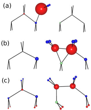
We calculate the lattice thermal conductivity in S-, Se- and Te- doped GaAs. We consider four different defect structures in each case. We study the defect, where the impurity atom simply replaces the As atom in the zincblende structure, and the more complex broken-bond (BB) and - and -cation-cation-bond (CCB) DX-center structures. All the structures are fully relaxed, and the resulting configurations for GaAs:S are shown in Fig. 1. The optimized atomic structures of the BB-DX and -CCB-DX defects [Fig. 1(b and d)] closely reproduce those in previous reports.ParkPRB96 ; DuPRB05 ; MaPRB13 The -CCB-DX case in Fig. 1(c) is slightly different from the previously reported structureParkPRB96 ; DuPRB05 in that we find an asymmetric relaxation. The energy of our asymmetric structure is only lower than the previously reported structure. However, the asymmetric relaxation is necessary for the -CCB-DX center to be mechanically stable and to obtain purely real phonon frequencies.
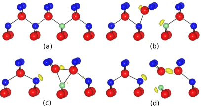
The ELFsELF for all the DX centers are also shown in Fig. 1. The ELF yields an estimate of the local effect of Pauli repulsion on the behavior of the electrons and allows a real-space mapping of the core, bonding and non-bonding regions in a crystal as well as an understanding of the nature of bonding and the presence of lone pairs of electrons.Savin_Angew97 The formation of electronic lone pairs plays an important role in the stabilization of the individual DX center structures.Onopko01 Fig. 1(b) illustrates how, in the BB-DX case, the bond between the dopant and Ga atom breaks due to the formation of lone pairs on the dopant and the neighboring Ga atom and how the repulsion from the negatively charged sulfur defect causes the neighboring Ga to occupy an interstitial position. For the - and -CCB-DX centers, a similar picture of bond breaking is observed, as shown in Fig. 1(c) and (d). In this case, lone pairs are formed on the dopant and on an As atom. Moreover, the ELF reflects a strong cation-cation (Ga-Ga) covalent bond. Thus, complex lattice relaxations around the dopant are involved in the DX centers which, as mentioned above, are believed to have a strong effect on thermal conductivity.
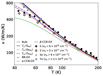
The thermal conductivity is calculated for all four defect structures for S-, Se- and Te-doped GaAs. The results for the defect in S-, Se- and Te-doped GaAs and for the DX centers of GaAs:S are shown in Fig. 2 and compared with the experimental values obtained from single crystal samples.VuillermozPSSA77 ; CarlsonJAP65 The calculated thermal conductivity of pristine bulk GaAs is also plotted as a reference. In the region above , where the thermal conductivity is dominated by three-phonon processes, the thermal conductivities for the defect-laden structures are very close to each other and to the bulk values, and are inversely proportional to the temperature. Theoretical calculations are performed at defect concentrations corresponding to the experimentally reported carrier concentrationsVuillermozPSSA77 ; CarlsonJAP65 and it can be seen that the thermal conductivities of bulk and -defect-containing GaAs are almost identical over the whole range of temperature. Even in the low-temperature region () the influence of the defects is small. The experimental values for Se- and Te-doped samplesCarlsonJAP65 only show signs of weak defect scattering and match well with our calculated values for the simple substitutional defect. On the other hand, the calculated thermal conductivity for different DX centers in GaAs:S deviates significantly from the bulk thermal conductivity in the low-temperature region. Fig. 2 shows that a similar suppression of the low-temperature lattice thermal conductivity is observed experimentally for GaAs:S.VuillermozPSSA77 This clearly points to the DX centers having very different strengths as phonon scatterers. It is interesting to note that a similar depression of the experimental thermal conductivity in HgSe in the temperature range from was attributed to a resonance in the phonon-defect scattering rates.Nelson_PRL69 We have also considered boundary scattering as a possible alternative explanation of the low temperature thermal conductivity. However, to obtain a satisfactory agreement with experiment (see supplementary material), average grain sizes below 1 mm were necessary, which seems unreasonable as the experiments were performed on high quality single crystals with reported sizes around 25 mm.VuillermozPSSA77
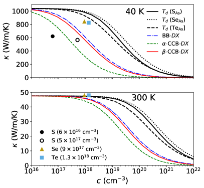
In the experimental reports used as sources for the data in Fig. 2 there is no information about the type of defect present in the sample. While the carrier concentration obtained from Hall coefficient measurements gives an indication of the defect concentration it may not directly correspond to the actual values. This will be the case when DX centers and substitutional defects, which act as acceptor and donors respectively, compensate each other. We have previously proposed a compensation scenario to explain the thermal conductivity of FeSi.Stern_PRB18 In Fig. 3 we show the variation of thermal conductivity as a function of carrier concentration for all the defects considered and for the DX centers of GaAs:S at two different temperatures, , and . Among the defects in Fig. 3, the Te-doped one leads to the largest reduction of thermal conductivity, followed by S and Se. This can be understood simply in terms of the mass difference between As and the doped atom, which takes values of , and for the S, Se, and Te atoms, respectively. The thermal conductivity is substantially lowered by BB-DX, -CCB-DX and -CCB-DX GaAs:S centers, in that order. At the low carrier concentrations found in experimental measurements, the difference is only observable at low temperatures where phonon scattering by DX centers dominates. It can be seen that the experimental data for GaAs:S ( W/mK at 40 K) can be explained by the presence of DX-centers at concentrations between cm-3 and cm-3. This would fit very well into a picture where the Fermi level is pinned to the center of the band gap by compensating and oppositely charged defects. This would lead to both a low defect concentration, due to the 1.5 eV band gap of GaAs, and to an even lower carrier concentration, due to the compensation between -donor and DX-acceptor defects. On the other hand, if the thermal conductivity were to be explained by substitutional -defects alone, a defect concentration close to 1020 cm-3 would be necessary, Fig. 3. It is thus clear that a picture of uncompensated substitutional defects cannot simultaneously explain the low carrier concentration and the reduced thermal conductivity. Similar behaviors are observed in the cases of Se and Te, and the corresponding figures are shown in the supplementary material. More specifically, the lowest thermal conductivities for a given concentration are obtained for the -CCB-DX and -CCB-DX centers in Se and Te, respectively.
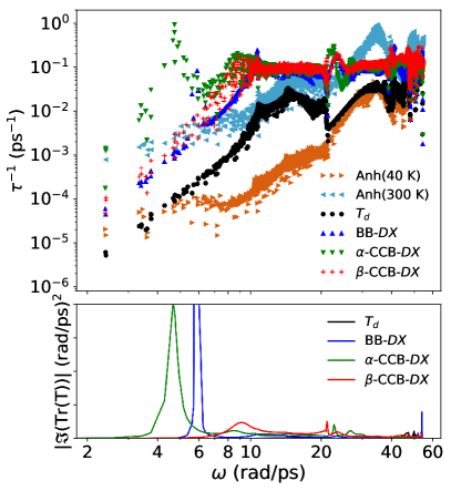
A lowered thermal conductivity points to more intense phonon scattering. Fig. 4 shows the scattering rates due to defects at a hypothetical concentration of and the trace of the imaginary part of the matrix for the and DX centers of GaAs:S. The anharmonic scattering rates at and are shown in order to illustrate the dominance of different scattering mechanisms at different temperatures. Most noticeably, the scattering rates caused by the -CCB-DX exhibit a prominent peak at a frequency of . This peak is the signature of resonant phonon scattering and perfectly matches the corresponding peak in the elements of the matrix. In fact, a marked peak in the imaginary part of the trace of the scattering T matrix has been shown to be a straightforward way to identify the resonance scattering.Katre_PRL17 ; Dongre_JMCC18 A very sharp peak also appears in the BB-DX case at about , whereas the anomalously high scattering rates of -CCB-DX are mainly found around 8 rad/ps, close to where the transverse acoustic band of GaAs enters the edge of the Brillouin zone.Arrigoni_PRB18 As can be seen by comparing Figs. 3 and 4, the order of magnitude of the scattering rates in the low-frequency range has a significant impact on the thermal conductivity. It is clear that all the DX-centers have a higher scattering rate, and result in a lower thermal conductivity, than the substitutional defect. It is also clear that the resonance for the BB-DX falls in such a narrow frequency range that it affects the thermal conductivity much less than the large broad peak found in case of the -CCB-DX. In the case of Se, we observe a similar trend in the thermal conductivity, likewise explained by the magnitude of the scattering rates in the low-frequency region (Figs. 2 and 3, supplementary material). For Te, we observe a different trend, where the lowest value of the thermal conductivity is registered for the -CCB-DX center (Fig. 2, supplementary material). However, this can also be understood from the scattering rates (Fig. 3, supplementary material) since -CCB-DX introduces scattering rates that are two orders of magnitude higher than those of BB-DX and -CCB-DX for the same concentration. In the following we will look into the origin of the narrow peak.
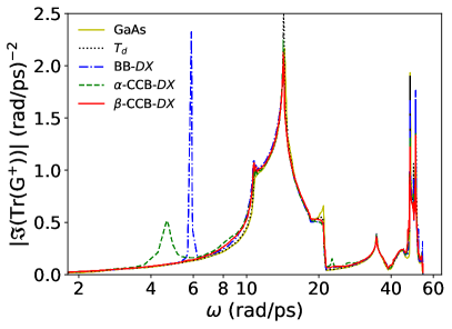
To dig further into the nature of the resonances, we have calculated the Green’s function of the perturbed system, , via the Dyson equation, Eq. (8). The trace of the imaginary part of the projection of on the degrees of freedom of the supercell is shown in Fig. 5 as representative of the phonon density of states (DOS) of the perturbed system. Besides the propagating modes inherited from the unperturbed structure, the plot shows a clear peak at each frequency where a resonance is observed in the scatterings rates. Such peaks hint at more localized vibrations as causes of those resonances. To confirm this inference, in Fig. 6 we plot the individual DOS projected on the atoms making up the defect at a frequency corresponding to the peak, with each atom represented by a sphere with a volume proportional to its relative contribution to the phonon DOS. It can be seen that the -like peak for BB-DX (see Figs. 4 and 6) corresponds to modes almost entirely localized around the Ga atom that is displaced to an interstitial position. The broader peak in the case of -CCB-DX is associated to an intermediate degree of localization made possible by the asymmetric structural relaxations around the dopant. The interaction (i.e., scattering) of incident phonons with those intermediately localized modes strongly hinders thermal transport. Finally the broad peak observed for -CCB-DX is quite delocalized over the surroundings of the defect.
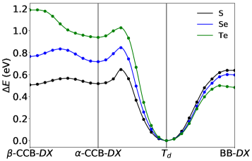
In a previous study, we posited that two or more close energy minima in the energy landscape are a necessary condition for having resonant phonon scattering since they create very flat-bottomed energy valleys.Dongre_JMCC18 Thus, we calculate the barriers to transitions between different configurations using the NEB method. Fig. 7 shows the results for all structures and all dopants. It can be seen that the defect has the lowest energy among all the impurities and the DX centers are thus only locally stable. We constructed intermediate structures between all four defects. However, we found that the paths connecting the CCB- and BB-DX defects relax to the structure, which also seems reasonable considering the structures in Fig. 1. Still, the energy minima corresponding to the DX centers are very flat. This is in line with our earlier analysis of the conditions necessary for finding an IFC perturbation large enough to produce resonances in the scattering rates in the low-frequency region for the DX centers.Dongre_JMCC18
IV Conclusions
The formation of DX centers in GaAs is explained by investigating the electron localization function, and we conclude that the lone pair electrons play a crucial role in determining their structure. We performed ab initio calculations of the lattice thermal conductivity of GaAs in the presence of defects or DX centers induced by S, Se, and Te dopants. The calculated thermal conductivity shows good agreement with existing measurements.
The asymmetric relaxation in the DX centers causes strong perturbations in the IFCs resulting in intense phonon scattering even at low defect concentrations. The results thereby strengthen the emerging understanding of how the lattice thermal conductivity can be used to unveil the dominant defects in semiconductors.
The resonances in the phonon scattering rates were attributed to localized vibrational modes in the perturbed system associated to the structural distortions. These localized modes are connected to flat valleys in the energy landscape such as those emerging from degenerate minima. Overall, we show the dramatic influence of the local atomic structure of the dopant on a macroscopic quantity like the thermal conductivity and illustrate how to take it into account, which might be useful for advanced semiconductor design.
ACKNOWLEDGMENT
A. K. thanks Bonny Dongre and Marco Arrigoni for their help in the calculations. The authors acknowledge support from the European Union’s Horizon 2020 Research and Innovation Action, Grant No. 645776 (ALMA), and from the French (ANR) and Austrian (FWF) Science Funds, project CODIS (ANR-17-CE08-0044-01 and FWF-I-3576-N36). We also thank the Vienna Scientific Cluster for providing the computational facilities (project number 70958: ALMA).
References
- (1) S. M. Sze and K. K. Ng, Physics of semiconductor devices, John wiley & sons, 2006.
- (2) K. F. Brennan, The physics of semiconductors: with applications to optoelectronic devices, Cambridge university press, 1999.
- (3) H. J. Queisser and E. E. Haller, Science 281, 945 (1998).
- (4) J. Callaway and H. C. von Baeyer, Phys. Rev. 120, 1149 (1960).
- (5) A. Katre, J. Carrete, B. Dongre, G. K. H. Madsen, and N. Mingo, Phys. Rev. Lett. 119, 075902 (2017).
- (6) A. Katre, J. Carrete, T. Wang, G. K. H. Madsen, and N. Mingo, Phys. Rev. Materials 2, 050602 (2018).
- (7) C. A. Polanco and L. Lindsay, Phys. Rev. B 98, 014306 (2018).
- (8) P. M. Mooney, J. Appl. Phys. 67, R1 (1990).
- (9) R. O. Carlson, G. A. Slack, and S. J. Silverman, J. Appl. Phys. 36, 505 (1965).
- (10) P. L. Vuillermoz, J. Jouglar, A. Laugier, and H. R. Winteler, Phys. Status Solidi (a) 41, 561 (1977).
- (11) B. Dongre, J. Carrete, A. Katre, N. Mingo, and G. K. H. Madsen, J. Mater. Chem. C 6, 4691 (2018).
- (12) C. H. Park and D. J. Chadi, Phys. Rev. B 54, R14246 (1996).
- (13) M.-H. Du and S. B. Zhang, Phys. Rev. B 72, 075210 (2005).
- (14) J. Ma and S.-H. Wei, Phys. Rev. B 87, 115210 (2013).
- (15) A. D. Becke and K. E. Edgecombe, J. Chem. Phys. 92, 5397 (1990).
- (16) G. Henkelman, B. P. Uberuaga, and H. Jónsson, J. Chem. Phys. 113, 9901 (2000).
- (17) J. Carrete, B. Vermeersch, A. Katre, A. van Roekeghem, T. Wang, G. K. H. Madsen, and N. Mingo, Computer Physics Communications 220, 351 (2017).
- (18) S.-i. Tamura, Phys. Rev. B 30, 849 (1984).
- (19) N. Mingo, K. Esfarjani, D. A. Broido, and D. A. Stewart, Phys. Rev. B 81, 045408 (2010).
- (20) P. E. Blöchl, Phys. Rev. B 50, 17953 (1994).
- (21) G. Kresse and J. Furthmüller, Phys. Rev. B 54, 11169 (1996).
- (22) G. Kresse and D. Joubert, Phys. Rev. B 59, 1758 (1999).
- (23) E. D. Pierron, D. L. Parker, and J. B. McNeely, Acta Crystallogr. 21, 290 (1966).
- (24) J. B. Mullin, B. W. Straughan, C. M. H. Driscoll, and A. F. W. Willoughby, J. Appl. Phys. 47, 2584 (1976).
- (25) O. H. Nielsen and R. M. Martin, Phys. Rev. B 32, 3792 (1985).
- (26) A. Togo and I. Tanaka, Scr. Mater. 108, 1 (2015).
- (27) W. Li, J. Carrete, N. A. Katcho, and N. Mingo, Comp. Phys. Commun. 185, 1747–1758 (2014).
- (28) P. Lambin and J. P. Vigneron, Phys. Rev. B 29, 3430 (1984).
- (29) A. Savin, R. Nesper, S. Wengert, and T. F. Fässler, Angew. Chemie Int. Ed. 36, 1808 (1997).
- (30) D. Onopko and A. Ryskin, Semiconductors 35, 1223 (2001).
- (31) D. A. Nelson, J. G. Broerman, E. C. Paxhia, and C. R. Whitsett, Phys. Rev. Lett. 22, 884 (1969).
- (32) R. Stern, T. Wang, J. Carrete, N. Mingo, and G. K. H. Madsen, Phys. Rev. B 97, 195201 (2018).
- (33) M. Arrigoni, J. Carrete, N. Mingo, and G. K. H. Madsen, Phys. Rev. B 98, 115205 (2018).
- (34) C. Persson, Y.-J. Zhao, S. Lany, and A. Zunger, Phys. Rev. B 72, 035211 (2005).