Microring resonators on a suspended membrane circuit for atom-light interactions
Abstract
Creating strong coupling between quantum emitters and a high-fidelity photonic platform has been a central mission in the fields of quantum optics and quantum photonics. Here, we describe the design and fabrication of a scalable atom-light photonic interface based on a silicon nitride microring resonator on a transparent silicon dioxide-nitride multi-layer membrane. This new photonic platform is fully compatible with freespace cold atom laser cooling, stable trapping, and sorting at around 100 nm from the microring surface, permitting the formation of an organized, strongly interacting atom-photonic hybrid lattice. We demonstrate small radius (around 16 ) microring and racetrack resonators with a high quality factor () of , projecting a single atom cooperativity parameter () of 25 and a vacuum Rabi frequency () of MHz for trapped cesium atoms interacting with a microring resonator mode. We show that the quality factor is currently limited by the surface roughness of the multi-layer membrane, grown using low pressure chemical vapor deposition (LPCVD) processes. We discuss possible further improvements to a quality factor above , potentially achieving single atom cooperativity parameter higher than 500 for strong single atom-photon coupling. Our microring platform may also find applications in on-chip solid-state quantum photonics.
I Introduction
Creating efficient atom-light nanophotonic interfaces with stably trapped atoms in their optical near-field can lead to a wide range of applications in quantum optics, quantum communications, and quantum many-body physics O’brien et al. (2009); Cirac and Kimble (2017); Chang et al. (2018). Optical nanofibers Vetsch et al. (2010); Goban et al. (2012); Kato and Aoki (2015); Sorensen et al. (2016); Corzo et al. (2016), photonic crystal waveguides Goban et al. (2015), and cavities Thompson et al. (2013); Tiecke et al. (2014) are exemplary platforms that have recently demonstrated atom trapping and large atom-light interactions in the evanescent field of their guided modes. Key enabling features for enhanced coupling are sub-diffraction transverse confinement of guided photons and enhanced photonic density of states, achieved either through forming micro- or nano-scale Fabry-Perot cavities or through slow light effects in photonic crystal waveguides. They permit several far-off resonant optical trapping schemes Grimm et al. (2000) in the near-field, such as two-color evanescent field traps Le Kien et al. (2004); Balykin et al. (2004); Lacroûte et al. (2012), side-illuminating optical traps Thompson et al. (2013); Goban et al. (2015); Pérez-Ríos et al. (2017), or a hybrid trap formed by Casimir-Polder vacuum force and a single-color optical potential in photonic crystal waveguides Hung et al. (2013); Gonzalez-Tudela et al. (2015). With near field (100 nm) trapping above the dielectric surface, it is generally expected that tens to more than a hundred-fold increase in atom-photon coupling rate may be found for a trapped atom in a nanophotonic platform compared to those realized in mirror-based optical cavities and resonators.
On the other hand, achieving coherent quantum operations with high-fidelity requires ultra-low optical loss in the host dielectric nanostructures Douglas et al. (2015); Gonzalez-Tudela et al. (2015), and has remained a challenge. In cavity quantum electrodynamics (QED), the figure of merit for quantum coherence is favored by a large single atom cooperativity parameter , requiring that the atom-photon coupling strength is large compared to the geometric mean of the photonic loss rate () and the atomic radiative decay rate into freespace (). For a perfect quantum emitter, (assuming a spherical symmetric dipole) and depends solely on the ratio between the quality factor of the photonic mode (of frequency and freespace wavelength ) and the effective mode volume , which is inversely proportional to the guided-mode photon energy density at the atomic trap location. State-of-the-art high-Q nanophotonic platforms have yet to achieve cooperativity parameters due to limited that stems mostly from fabrication imperfections. For example, and is reported recently for a photonic crystal cavity Tiecke et al. (2014) and an atom-induced cavity near the band edge of a photonic crystal waveguide Hood et al. (2016); Douglas et al. (2015) that are tailored for coupling with alkali atoms at resonant wavelengths ranging from nm at rubidium D2-line to nm at cesium D1-line. There are multiple schemes in existence for boosting in atom-nanophotonic platforms Chang et al. (2018). For comparison, monolithic micro-photonic resonators such as silica micro-toroids Aoki et al. (2006), bottles O’Shea et al. (2013), and spheres Shomroni et al. (2014) or silicon nitride micro-disks Barclay et al. (2006) are other photonic resonator structures with ultrahigh quality factors but with large for transit atoms in time-of-flight. The prospect of direct laser cooling and atom trapping in their optical near field has remained elusive, partially due to geometrical constraints and limited optical access through the dielectric structures and their substrates Alton (2013), if present.
In this paper, we report a planar-type microring photonic structure and its racetrack-variant design capable of simultaneous realizations of strong confinement for large atom-photon coupling rate, experimentally accessible atom trapping and sorting schemes, and high , serving as a coherent, scalable atom-photon quantum interface. Our implementation is based on silicon nitride microring resonators that have recently achieved ultrahigh quality factors in telecom optical wavelength band Xuan et al. (2016); Ji et al. (2017) and close to Cs atomic spectroscopy bands Kaufmann et al. (2018). We adapt the design to geometries tailored for cavity QED with neutral atoms and address major challenges that need to be overcome. We enable full optical access for laser cooling and trapping of alkali atoms, e.g. atomic cesium, directly on a microring by fabricating it on a transparent membrane substrate. Moreover, we investigate various trapping schemes including two-color evanescent field trap and top-illuminating optical tweezer trap at tunable distances around 100 nm above a resonator waveguide, as well as the combination of both schemes for atom array sorting.
II Overview of the platform
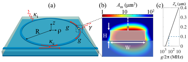
Figure 1 shows the schematics of our resonator platform. The microrings are fabricated on top of a suspended SiO2-Si3N4 multi-layer membrane, formed by a m-thick SiO2 (silicon dioxide) layer and a nm-thick Si3N4 (silicon nitride) bottom-layer that can provide high tensile stress after being released from a silicon substrate to form a large window around an area of mm 8 mm; see Fig. 2. The high tensile stress offered by the nitride bottom layer is necessary to preserve the optical flatness of the membrane. The transparent membrane allows laser beams to be sent from either top or bottom sides of the microring structure, allowing cold atoms to be directly laser cooled, trapped, and transported on the surface of a microring resonator Kim et al. (2019).
Due to its higher mode field intensity above the surface of the resonator waveguide (Supplement 1 Sec. 1-A), we utilize the fundamental transverse-magnetic (TM) mode for creating atom-light coupling. The cross section of the resonator waveguide is chosen for sufficient evanescent field strength above the waveguide surface while maintaining high . The small radius of the microring m ensures a moderately small mode volume , where is the circumference of the ring and is the effective mode area defined as
| (1) |
Here denotes the transverse atomic location in cylindrical coordinates, is the dielectric function of the microring structure, and is the TM-mode electric field. Figure 1 (b) plots the cross section of the effective mode area of a TM-mode at cesium D1-line nm. A moderately small mode area m2 can be achieved when an atom is placed at around nm above the microring surface, projecting a mode volume of m3, single-photon vacuum Rabi frequency MHz, and a cooperativity parameter . Achieving high in such a small microring can thus make this platform well-suited for on-chip cavity QED experiments with high fidelity.
A linear bus waveguide is fabricated next to an array of microrings to couple to the clockwise (CW) and counter-clockwise (CCW) resonator modes. Away from the microring coupling region, the bus waveguide is tapered and extends all the way towards the edge of the transparent window where the waveguide is then embedded in a dioxide (or vacuum) top-cladding layer.
As shown in Fig. 2, a U-shaped fiber groove is fabricated for epoxy fixture of a lensed optical fiber, which is edge-coupled to the bus waveguide with % (or % with vacuum cladding) single-pass coupling efficiency as expected through our finite-difference-time-domain (FDTD) calculations cit (a). We have currently achieved % coupling efficiency with vacuum cladding. The lensed fiber, the edge-coupled bus waveguide, and an array of coupled microrings form a complete package of high-fidelity atom-light nanophotonics interface; see Fig. 2.
III Fabrication of microring membrane circuit and optical measurements
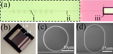
Figure 2 (a-b) show the optical image of a fabricated membrane optical circuit (see Kim et al. (2019) for fabrication procedures). SEM images of microring and racetrack resonators on the membrane with coupling waveguide buses are shown in Fig. 2(c-d).
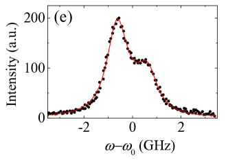
We characterize the quality factors near cesium D1 line by scanning the frequency of the coupled TM-mode and image the scattered light from individual rings on a charge-coupled-device (CCD) camera. The resonant frequency of the microring, , has been thermally tuned by a freespace laser beam heating the silicon part of the optical circuit in vacuum Tiecke et al. (2014). Figure 2(d) shows a sample measurement. Double resonant peaks have been observed due to coherent back-scattering effect from fabrication imperfections that mixes the CW and CCW modes and creates an energy splitting (see Supplement 1 Sec. 1-B). Our measured CCD counts can be well fitted by a coupled-mode model Srinivasan and Painter (2007) that captures mode-splitting and the peak asymmetry (see also Eq. 2 and Supplement 1 Sec. 1-B). The fit gives total photon loss rate 1.01 GHz, corresponding to an under-coupled quality factor of due to waveguide coupling rate smaller than the intrinsic loss rate .
Using the measurement results and the fabricated geometry m, we project the single atom cooperativity parameter to be , calculated using MHz; under the same and the geometry presented in Fig. 1, we project with MHz. We note that there is still much room for improvement. Below we discuss in detail the optical loss analysis and optimization for maximizing cooperativity .
III.1 Current fabrication limit and mitigation methods
Currently, surface scattering dominates the photon loss in our fabricated microrings; see also Supplement 1 Sec. 3-A for fundamental limits of the microring platform regarding material absorption. We have characterized the surfaces of the multi-layer film using atomic force microscopy (AFM) and obtained the root-mean-squared roughness nm and the correlation length nm for the top nitride layer. For the bottom surface roughness of the microring, we infer from the surface quality of the dioxide middle layer, which we measured nm. We estimate the edge roughness and correlation length to be around nm by employing multipass e-beam writing technique Ji et al. (2017); Roberts et al. (2017) and optimized inductively coupled-plasma reactive-ion etching process with CHF3/O2 gas chemistry Krückel et al. (2015); Ji et al. (2017); Roberts et al. (2017). In Supplement 1 Sec. 3-B, we adopt a volume current method to model the scattering loss rate due to the measured surface roughness Borselli et al. (2005). Our result indicates that is in reasonable agreement with our measured quality factor.
Due to the major roughness incurred in the LPCVD-deposited dioxide layer, we note that the surface roughness of the microring is around three times worse than a typical single layer nitride deposited on a silicon wafer or on a thermally grown dioxide film. Possible improvements can be made by using a chemical mechanical polishing (CMP) technique to reduce the surface roughness in the top nitride layer and the middle dioxide layer as well. It has been reported that the surface roughness and the correlation length of a nitride thin film can be greatly reduced down to nm and nm from its original rough surface Ji et al. (2017). Alternatively, the edge roughness and correlation length may be reduced to nm and nm by using a plasma-assisted resist reflow technique Porkolab et al. (2014). These immediate technological improvements permit a potential 10-fold increase in , as will be discussed below.
III.2 Q/Vm optimization
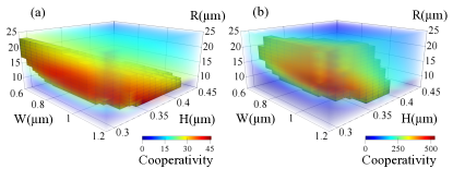
Given the characteristics of the surface quality and edge roughness, we perform finite element method (FEM) analysis cit (b) to obtain a geometrical design that maximizes , concerning the dominant losses including the surface scattering loss and the waveguide bending loss. By scanning the cross-section and the radius of the microring, it is observed that the waveguide cross-section cannot be reduced indefinitely due to the constraint of surface scattering. Similarly, the radius of the ring is constrained to be above m due to larger bending loss and scattering loss occurring at the sidewalls at larger bend curvature.
In Fig. 3, we plot the cooperativity parameter as a result of the scan, assuming an atom is trapped at nm. With the surface roughness at its current value, as in fig. 3(a), is maximized when the waveguide geometry tends towards larger cross section (), which reduces surface scattering, and smaller radius , which reduces the mode volume. The best projection uses a smaller ring m than in our current design and m. For reduced surface roughness, as in Fig. 3(b), a resonator geometry of m, as shown in Fig. 1, can achieve . The projected cooperativity reaches , an almost 12 times improvement from our current optimal value. Similarly, a fundamental transverse-electric (TE) mode can also be optimized with a different geometry, giving higher but with a lower optimal due to larger .
IV Atom trapping in the optical nearfield of the microring platform
We now discuss two schemes, both capable of creating tight far off-resonant optical traps for cold atoms around nm above the top surface of the microring. While either scheme can function fully independently, we discuss the combination of both schemes for atom array assembly on a microring (racetrack) resonator.

IV.1 State-insensitive two-color evanescent field trap
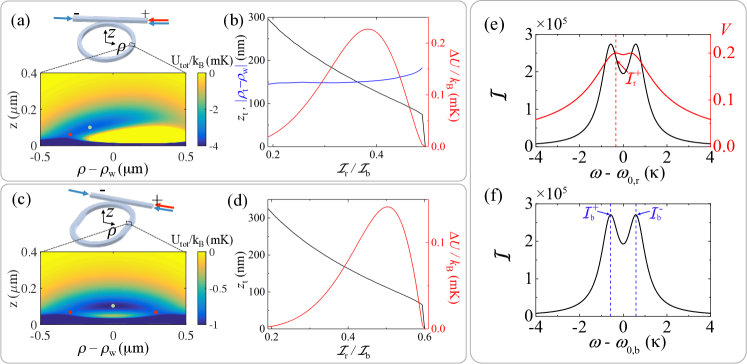
The evanescent field trapping scheme shares similarities with those realized in nano-fiber traps Le Kien et al. (2004); Lacroûte et al. (2012), and proposed in nanophotonic waveguides Meng et al. (2015); Stievater et al. (2016). The trap is formed by two TM modes excited near the ‘magic’ wavelengths nm and nm, so that they do not create differential light shifts in the laser cooling transition of cesium (Supplement 1 Sec. 2). Here, (frequency ) is blue-detuned from major optical transitions in the ground state, creating strongly repulsive optical force within a short range near the dielectric surface. (frequency ) is red-detuned, leading to an attractive force with longer decay length than that of the -mode. The combination of both modes creates a stable trap above the waveguide surface; see Fig. 4.
Along the microring, coherent back-scattering mixes the CW and CCW counter-propagating modes and converts an otherwise smooth evanescent field intensity profile into a standing wave pattern just like an optical lattice (Supplement 1 Sec. 1-B). An optical lattice potential can provide strong longitudinal trap confinement along the microring. Exciting the resonator from either end of the coupling waveguide bus with power and frequency near a resonance creates an electric field with a corrugated intensity profile
| (2) |
where the sign is given by the direction of bus waveguide coupling that excites opposite mixtures of the resonator modes (Supplement 1 Sec. 1-D); the sign flip is necessary due to coherent back-scattering. Here is a near-resonance energy build-up factor, with and a back-scattering rate ,
| (3) |
is the normalized mode field amplitude, giving , is the propagation wavenumber, is the arc length along the microring waveguide, and is a frequency dependent phase shift. The visibility of the corrugation is given by
| (4) |
where the amplitude factor for a TM-mode (Supplement 1 Sec. 1-B). For the simplicity of discussions, we assume the waveguide parameters are equal for the two color modes.
To form a homogeneous lattice trap along the resonator, we eliminate the standing wave pattern in the mode to avoid incommensurate alignment between the blue-repulsive node and the red-attractive anti-node in the lattice potential. As shown in Fig. 4, we couple blue-detuned light from either end (+ and ) of the waveguide bus with symmetric detuning about to completely cancel the potential corrugation (Eq. 2) cit (c). We note that a large detuning between the modes is necessary to eliminate their interference contribution to the trap potential.
We calculate the two-color evanescent field trap potential using the incoherent sum of two-color potentials as
| (5) |
where (a.u.; in atomic unit) and (a.u.) are atomic dynamic scalar polarizabilities at frequencies and , respectively. Similarly, are the excited mode fields, and are energy build-up factors of the two color modes (see Fig. 4 (e, f)); is the wave number of the red mode, and is shifted to center on a lattice site.
The two-color evanescent field trap can be made state-insensitive, that is, independent of the Zeeman sublevels of cesium ground state atoms. We note that the vector light shift is completely canceled in the presented coupling scheme Lacroûte et al. (2012), as discussed in Supplement 1 Sec. 2-C. Thus, we only include the scalar light shift in Eq. (5).
Figure 4(a) shows sample potential cross sections in a transverse plane above the microring. Due to finite curvature of the microring waveguide that results in non-equal center shifts of the two color modes, the trap center is shifted inwards by nm and the trap axes are rotated. To avoid trap distortion, a racetrack resonator design [Fig. 4(c)] can be employed, where a symmetric trap can be found above the linear segments of the racetrack. The trap centers in Fig. 4(a,c) are nm on a microring and nm on a racetrack, respectively, where is the top surface center of the microring (racetrack) waveguide.
To illustrate that the trap is strong enough against the atom-surface attraction, we have included in Fig 4 the contribution of a Casimir-Polder potential for , where Hzm4 is for cesium atom-Si3N4 surface coefficient and nm is an effective wavelength Stern et al. (2011). The total trap potential
| (6) |
is dominated by only when nm. Here, the trap opens at potential saddle points near nm for a ring and nm for a racetrack; defines the trap depth , which is K in Fig. 4(a,c), and is 10 times larger than the typical temperature of laser-cooled cesium atoms.
The energy build-up factors used to calculate the trap on the microring (racetrack) in Fig. 4(a,c) are () for the mode and () for the modes, respectively. Using the coupling scheme and parameters associated with Fig. 4(e,f), the required total power is W (56 W) for and W (W) for modes in a microring (racetrack), respectively.
We note that by adjusting the power ratio of the two color modes, can be moved away from or pulled closer to the waveguide surface. In Fig. 4(b,d), we keep fixed while tuning the ratio (or ) and show that the trap center can be tuned from nm to nm. Meanwhile, remains fairly unchanged. This important feature would allow us to initiate atom trapping and sorting at nm and perform atom-light coupling at nm, discussed later.
Figure 5 shows the lattice potential along the axial position of a microring and a racetrack, plotted using the cross sections of in the planes of and , respectively. The low visibility (Fig. 4(e)) in the attractive TM-mode keeps the lattice potential nearly attractive everywhere along the resonator until very close to the resonator waveguide surface nm. This feature allows atoms to traverse freely along the resonator without seeing strong potential barrier until they are cooled into individual lattice sites at nm.
IV.2 Top-illuminating optical potential
Illuminating the microring from the top surface using a red-detuned beam (wavelength ) can also create a tight optical potential due to the top-illuminating beam interfering with its reflection from the microring structure (Fig. 6). The trap site closest to the dielectric surface, typically within a distance , can be utilized for trapping atoms in the near-field region of the resonator mode. Once an atom is trapped, the top-illuminating beam can also be steered in the horizontal plane to transport and organize atoms along the microring. This simple scheme need not have trapping light guided by the resonator, and can be universally applied to any dielectric structures with finite surface reflectance. The strength and position of the first trap site can in principle be finely adjusted through geometrically tuning the phase shift of the reflected light. In fact, this method has been successfully implemented in a number of pioneering experiments trapping atoms on suspended nanostructures Thompson et al. (2013); Goban et al. (2015), although fully independent trap tuning cannot be achieved because the geometry of a nanostructure needs to be adjusted and its desired guided mode property is inevitably affected.
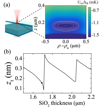
For the microring (racetrack) platform, trap condition in a top-illuminating potential can be finely adjusted independent of the waveguide properties, since multiple interfaces exist in the underlying membrane substrate. A desired trap condition can be realized simply by tuning the thickness of the dioxide or nitride layers in the membrane, as illustrated in Fig. 6.
Figure 6(a) shows a sample potential cross-section , where the optical potential is calculated by using a FDTD method cit (a) with a tightly focused Gaussian beam (nm) of a beam waist m and a power of mW projected from the top of the microring waveguide. The beam is polarized along , which is perpendicular to local waveguide orientation, to minimize reflection from the surface of the microring. In Fig. 6(b), we scan the thickness of the membrane, and illustrate a configuration such that the closest trap site to the microring surface is centered around nm, where is significantly smaller than nm, and the trap depth of K. With a tightly focused beam waist, the top-illuminating beam forms a tweezer-like optical potential, providing also strong transverse (along ) and axial (along ) confinements. The former is due to the waveguide width (), leading to a strong intensity variation in the transverse direction. The axial confinement, on the other hand, is ensured by the small beam waist of the tweezer beam. For the example given in Fig. 6(a), the trap frequencies are kHz.
IV.3 Trap loading and atom sorting along a microring (racetrack) resonator
In Kim et al. (2019), we have experimentally demonstrated that cold atoms can be directly laser-cooled on a membrane optical circuit and loaded into a top-illuminating optical tweezer trap. We note that the presence of lattice potential along a tweezer trap likely reduces the probability for cold atoms to be cooled directly into the first site near the microring surface. Instead, multiple atoms may be randomly confined along the lattice of microtraps within a tweezer. An optical conveyor belt can be implemented to transport trapped atoms onto the microring surface Kim et al. (2019). By monitoring the transmission of a resonator mode tuned to atomic resonance, it is possible to transport trapped atoms onto the micro-ring surface with deterministic control.
On the other hand, a two-color evanescent field trap provides a smooth transverse potential landscape (along ), allowing a large number of laser-cooled atoms to be loaded uninterruptedly from freespace into the lattice potential at nm above the microring, which has recently been demonstrated in nanofiber traps Le Kien et al. (2004); Balykin et al. (2004); Lacroûte et al. (2012). Nonetheless, these trapped atoms should randomly fill the optical lattice without organization.
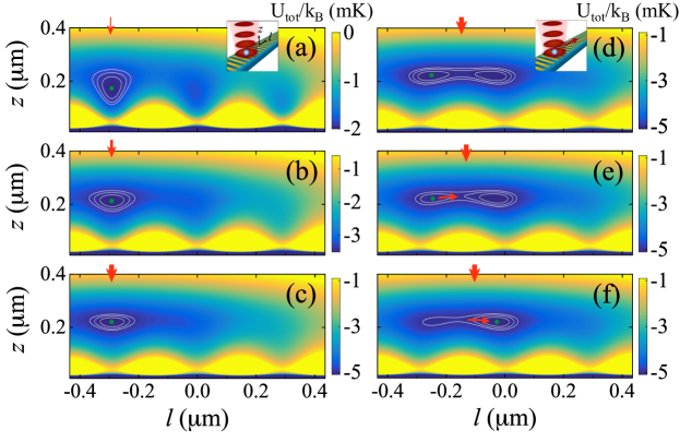
In Fig. 7, we illustrate how a tweezer trap can be used to sort trapped atoms in an evanescent field trap, similar to those in an optical lattice in freespace Barredo et al. (2016). To begin with, one may utilize the two-color evanescent field trap for initial atom loading into at nm. Following laser cooling, fluorescence imaging Kim et al. (2019) can be performed to determine the atomic distribution along the resonator. Once identifying the location of all trapped atoms, an optical tweezer trap can be ramped on to draw an atom into a new vertical position nm (Fig. 7(a-c)), and transport it along the resonator into a designated lattice site (Fig. 7(d-f); across multiple sites). Following transport, the tweezer beam can then be adiabatically ramped off, releasing the trapped atom back to the evanescent field trap at . Atom-sorting can be realized by reiterating the procedures to reorganize atoms in different trap sites.
V Conclusion and outlook
In this paper, we have demonstrated that microring and racetrack resonator platforms can be fabricated to be completely compatible with laser cooling and trapping with cold atoms and with reasonably high cooperativity parameters . This number can be further boosted by more than 10-fold with further fabrication improvements, thus holding great promises as an on-chip atom cavity QED platform. We have discussed two viable optical trapping schemes, both using magic wavelengths of atomic cesium, for localizing atoms around nm above the dielectric surface of a resonator waveguide structure. The combination of both schemes permits controlled atom transport along a resonator, allowing for the formation of an organized atom-nanophotonic hybrid lattice useful for collective quantum optics and many-body physics Chang et al. (2018); Hung et al. (2016).
Lastly, we note that although our emphasis is on coupling with cold trapped atoms, these microrings may also be adapted for coupling with solid state quantum emitters Wei et al. (2015); Saskin et al. (2019); Nandi et al. (2019), or with atomic thermal vapors Ritter et al. (2016, 2018). For emitters on the surface of a resonator waveguide and considering only the radiative losses, the effective mode volume and using our current fabricated structures, where n is the host refractive index for embedded quantum emitters. Improving to would lead to a projected that may be potentially useful for on-chip solid-state quantum photonics.
Acknowledgements
We acknowledge discussions from H. J. Kimble, S.-P. Yu, S. Bhave, M. Hosseini, S. Caliga, Y. Xuan, and B.-L. Yu. Funding is provided by the AFOSR YIP (Grant NO. FA9550-17-1-0298), ONR (Grant NO. N00014-17-1-2289) and the Kirk Endowment Exploratory Research Recharge Grant from the Birck Nanotechnology Center.
References
- O’brien et al. (2009) J. L. O’brien, A. Furusawa, and J. Vučković, Nature Photonics 3, 687 (2009).
- Cirac and Kimble (2017) J. I. Cirac and H. J. Kimble, Nature Photonics 11, 18 EP (2017).
- Chang et al. (2018) D. E. Chang, J. S. Douglas, A. González-Tudela, C.-L. Hung, and H. J. Kimble, Rev. Mod. Phys. 90, 031002 (2018).
- Vetsch et al. (2010) E. Vetsch, D. Reitz, G. Sague, R. Schmidt, S. T. Dawkins, and A. Rauschenbeutel, Phys. Rev. Lett. 104, 203603 (2010).
- Goban et al. (2012) A. Goban, K. S. Choi, D. J. Alton, D. Ding, C. Lacroute, M. Pototschnig, T. Thiele, N. P. Stern, and H. J. Kimble, Phys. Rev. Lett. 109, 033603 (2012).
- Kato and Aoki (2015) S. Kato and T. Aoki, Physical Review Letters 115, 093603 (2015).
- Sorensen et al. (2016) H. Sorensen, J.-B. Beguin, K. Kluge, I. Iakoupov, A. Sorensen, J. Muller, E. Polzik, and J. Appel, Physical Review Letters 117, 133604 (2016).
- Corzo et al. (2016) N. V. Corzo, B. Gouraud, A. Chandra, A. Goban, A. S. Sheremet, D. V. Kupriyanov, and J. Laurat, Physical Review Letters 117, 133603 (2016).
- Goban et al. (2015) A. Goban, C.-L. Hung, J. Hood, S.-P. Yu, J. Muniz, O. Painter, and H. Kimble, Physical Review Letters 115, 063601 (2015).
- Thompson et al. (2013) J. D. Thompson, T. G. Tiecke, N. P. de Leon, J. Feist, A. V. Akimov, M. Gullans, A. S. Zibrov, V. Vuletic, and M. D. Lukin, Science 340, 1202 (2013), ISSN 0036-8075, 1095-9203.
- Tiecke et al. (2014) T. G. Tiecke, J. D. Thompson, N. P. de Leon, L. R. Liu, V. Vuletic, and M. D. Lukin, Nature 508, 241 (2014), ISSN 0028-0836.
- Grimm et al. (2000) R. Grimm, M. Weidemüller, and Y. B. Ovchinnikov, in Advances in atomic, molecular, and optical physics (Elsevier, 2000), vol. 42, pp. 95–170.
- Le Kien et al. (2004) F. Le Kien, V. I. Balykin, and K. Hakuta, Physical Review A 70, 063403 (2004).
- Balykin et al. (2004) V. Balykin, K. Hakuta, F. Le Kien, J. Liang, and M. Morinaga, Physical Review A 70, 011401 (2004).
- Lacroûte et al. (2012) C. Lacroûte, K. Choi, A. Goban, D. Alton, D. Ding, N. Stern, and H. Kimble, New Journal of Physics 14, 023056 (2012).
- Pérez-Ríos et al. (2017) J. Pérez-Ríos, M. E. Kim, and C.-L. Hung, New Journal of Physics 19, 123035 (2017).
- Hung et al. (2013) C.-L. Hung, S. M. Meenehan, D. E. Chang, O. Painter, and H. J. Kimble, New Journal of Physics 15, 083026 (2013), ISSN 1367-2630.
- Gonzalez-Tudela et al. (2015) A. Gonzalez-Tudela, C.-L. Hung, D. E. Chang, J. I. Cirac, and H. J. Kimble, Nature Photonics 9, 320 (2015), ISSN 1749-4885.
- Douglas et al. (2015) J. S. Douglas, H. Habibian, C.-L. Hung, A. Gorshkov, H. J. Kimble, and D. E. Chang, Nature Photonics 9, 326 (2015).
- Hood et al. (2016) J. D. Hood, A. Goban, A. Asenjo-Garcia, M. Lu, S.-P. Yu, D. E. Chang, and H. Kimble, Proceedings of the National Academy of Sciences 113, 10507 (2016).
- Aoki et al. (2006) T. Aoki, B. Dayan, E. Wilcut, W. P. Bowen, A. S. Parkins, T. Kippenberg, K. Vahala, and H. Kimble, Nature 443, 671 (2006).
- O’Shea et al. (2013) D. O’Shea, C. Junge, J. Volz, and A. Rauschenbeutel, Physical review letters 111, 193601 (2013).
- Shomroni et al. (2014) I. Shomroni, S. Rosenblum, Y. Lovsky, O. Bechler, G. Guendelman, and B. Dayan, Science 345, 903 (2014).
- Barclay et al. (2006) P. E. Barclay, K. Srinivasan, O. Painter, B. Lev, and H. Mabuchi, Applied physics letters 89, 131108 (2006).
- Alton (2013) D. J. Alton, Ph.D. thesis, California Institute of Technology (2013).
- Xuan et al. (2016) Y. Xuan, Y. Liu, L. T. Varghese, A. J. Metcalf, X. Xue, P.-H. Wang, K. Han, J. A. Jaramillo-Villegas, A. A. Noman, C. Wang, et al., Optica 3, 1171 (2016).
- Ji et al. (2017) X. Ji, F. A. S. Barbosa, S. P. Roberts, A. Dutt, J. Cardenas, Y. Okawachi, A. Bryant, A. L. Gaeta, and M. Lipson, Optica 4, 619 (2017).
- Kaufmann et al. (2018) P. Kaufmann, X. Ji, K. Luke, M. Lipson, and S. Ramelow, in Conference on Lasers and Electro-Optics (Optical Society of America, 2018), p. JTu2A.72.
- Kim et al. (2019) M. E. Kim, T.-H. Chang, B. M. Fields, C.-A. Chen, and C.-L. Hung, Nature Communications 10, 1647 (2019).
- cit (a) https://www.lumerical.com.
- Srinivasan and Painter (2007) K. Srinivasan and O. Painter, Phys. Rev. A 75, 023814 (2007).
- Roberts et al. (2017) S. P. Roberts, X. Ji, J. Cardenas, A. Bryant, and M. Lipson, in Conference on Lasers and Electro-Optics (Optical Society of America, 2017), p. SM3K.6.
- Krückel et al. (2015) C. J. Krückel, A. Fülöp, T. Klintberg, J. Bengtsson, P. A. Andrekson, and V. Torres-Company, Opt. Express 23, 25827 (2015).
- Borselli et al. (2005) M. Borselli, T. J. Johnson, and O. Painter, Opt. Express 13, 1515 (2005).
- Porkolab et al. (2014) G. A. Porkolab, P. Apiratikul, B. Wang, S. H. Guo, and C. J. K. Richardson, Opt. Express 22, 7733 (2014).
- cit (b) https://www.comsol.com.
- Meng et al. (2015) Y. Meng, J. Lee, M. Dagenais, and S. Rolston, Applied Physics Letters 107, 091110 (2015).
- Stievater et al. (2016) T. H. Stievater, D. A. Kozak, M. W. Pruessner, R. Mahon, D. Park, W. S. Rabinovich, and F. K. Fatemi, Optical Materials Express 6, 3826 (2016).
- cit (c) Alternatively, one may also excite the blue-detuned mode via single end of the waveguide bus using a laser of finite line width (GHz) so that no coherent back-scattering can establish within the microring.
- Stern et al. (2011) N. P. Stern, D. J. Alton, and H. J. Kimble, New Journal of Physics 13, 085004 (2011), URL https://doi.org/10.1088%2F1367-2630%2F13%2F8%2F085004.
- Barredo et al. (2016) D. Barredo, S. d. Leseleuc, V. Lienhard, T. Lahaye, and A. Browaeys, Science 354, 1021 (2016), ISSN 0036-8075, 1095-9203.
- Hung et al. (2016) C.-L. Hung, A. González-Tudela, J. I. Cirac, and H. J. Kimble, Proceedings of the National Academy of Sciences 113, E4946 (2016), ISSN 0027-8424, 1091-6490.
- Wei et al. (2015) G. Wei, T. K. Stanev, D. A. Czaplewski, I. W. Jung, and N. P. Stern, Applied Physics Letters 107, 091112 (2015).
- Saskin et al. (2019) S. Saskin, J. Wilson, B. Grinkemeyer, and J. D. Thompson, Physical review letters 122, 143002 (2019).
- Nandi et al. (2019) A. Nandi, X. Jiang, D. Pak, D. Perry, K. Han, E. S. Bielejec, Y. Xuan, and M. Hosseini, arXiv preprint arXiv:1902.08898 (2019).
- Ritter et al. (2016) R. Ritter, N. Gruhler, W. Pernice, H. Kübler, T. Pfau, and R. Löw, New Journal of Physics 18, 103031 (2016).
- Ritter et al. (2018) R. Ritter, N. Gruhler, H. Dobbertin, H. Kübler, S. Scheel, W. Pernice, T. Pfau, and R. Löw, Physical Review X 8, 021032 (2018).
- Oxborrow (2007) M. Oxborrow, IEEE Transactions on Microwave Theory and Techniques 55, 1209 (2007), ISSN 0018-9480.
- Cheema and Kirk (2010) M. I. Cheema and A. G. Kirk, in COMSOL conference (2010).
- Pfeiffer et al. (2018) M. H. P. Pfeiffer, J. Liu, A. S. Raja, T. Morais, B. Ghadiani, and T. J. Kippenberg, Optica 5, 884 (2018).
- Ding et al. (2012) D. Ding, A. Goban, K. Choi, and H. Kimble, arXiv preprint arXiv:1212.4941 (2012).
- Payne and Lacey (1994) F. Payne and J. Lacey, Optical and Quantum Electronics 26, 977 (1994).
- Poulton et al. (2006) C. G. Poulton, C. Koos, M. Fujii, A. Pfrang, T. Schimmel, J. Leuthold, and W. Freude, IEEE Journal of selected topics in quantum electronics 12, 1306 (2006).
- Kuznetsov (1985) M. Kuznetsov, Journal of Lightwave Technology 3, 674 (1985), ISSN 0733-8724.
Appendix A Electric field profile and mode-mixing in a microring resonator
A.1 Mode profile in an ideal microring
Due to the small dimensions of our microring geometry, it supports only fundamental modes within the resonator waveguide at the wavelengths of our interest. A perfect microring supports resonator modes of integer azimuthal mode number , whose electric field can be written as , where the spatial field profile in cylindrical coordinates is
| (7) |
We additionally require that the mode field satisfies the normalization condition , where is the vacuum permittivity and is the dielectric function. Here, () are real functions and are independent of due to cylindrical symmetry. We note that the azimuthal field component is out of phase with respect to the transverse fields due to strong evanescence field decay and transversality of the Maxwell’s equation. The perfect resonator modes are traveling waves and the sign indicates the direction of circulation. The mode fields of opposite circulations are complex conjugates of one another . We can assign a propagation number , where is the arc length.
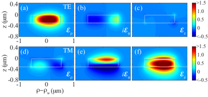
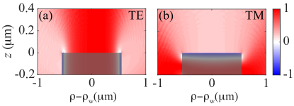
The electric field functions are evaluated using a software employing a finite element method (COMSOL) Oxborrow (2007); Cheema and Kirk (2010). Fig. A.1 shows the electric field components (in cylindrical coordinates) of the fundamental transverse electric (TE) and transverse magnetic (TM) resonator modes. The fields are slightly asymmetric across the center of the waveguide at due to finite curvature of the microring (radius m). We also note that the out-of-phase axial component is stronger in the TM-mode, resulting from stronger evanescent field along the axis where the waveguide confinement is strongly subwavelength.
A.2 Mode mixing in a microring
In the presence of fabrication imperfections, surface scatters induce radiation loss and mode mixing. The former, together with other intrinsic loss mechanisms (discussed in Borselli et al. (2005); Ji et al. (2017); Pfeiffer et al. (2018)), induces intrinsic resonator energy loss at a rate . The latter effect can be treated perturbatively, with photons scattered from one resonator mode into another. Assuming small dielectric irregularities in a high-Q resonator, only counter-propagating modes with identical azimuthal number can couple via back-scattering from the surface roughness (at a rate ). In this paper we obtain this back-scattering rate experimentally.
To understand mode-mixing and its impact on the resonator mode profiles, we apply well-established coupled mode theory Srinivasan and Painter (2007) for two counter propagating modes of interest. Using to denote the amplitude of the clock-wise (CW) and counter clock-wise (CCW) propagating resonator modes in a mode-mixed resonator field
| (8) |
we have the following coupled rate equation
| (9) |
where is the frequency detuning from the bare resonance , is the coherent back-scattering rate, and is a scattering phase shift. The total loss rate includes resonator intrinsic loss rate and the loss rate from coupling to the bus waveguide.
Due to the back-scattering terms in Eq. 9 mixing CW and CCW modes, a new set of normal modes are established whose rate equations are decoupled from each other and the frequencies of the new modes are shifted by and relative to the unperturbed resonance, respectively. The electric field of the mixed mode can be written as (), where
| (10) |
and we have dropped an overall factor for convenience. The fields in Eq. 10 should also satisfy the normalization condition. With the presence of back-scattering, the resonator mode polarization now becomes linear but is rotating primarily in the - (-) plane for TE (TM) mode along the microring.
A.3 Atom-photon coupling in a microring resonator
We consider the atom-photon coupling strength
| (11) |
where is the transition dipole moment, is the electric field polarization vector, , is the Planck constant divided by , and is the effective mode volume at atomic position ,
| (12) |
Here follows the definition Eq. 1 in the main text and is the circumference of the microring.
We note that the coupled modes in Eq. 11 can be the CW and CCW modes, that is , when . On the other hand, if , an atom should be coupled to a mixed mode with . Our microring platform corresponds to the latter case. We also note that the exact value of the transition dipole moment depends on the atomic location and dipole orientation. In the main text, we simply replace with the reduced dipole moment , where , and arrive at
| (13) |
A.4 Exciting the resonator mode via an external waveguide
If we consider exciting the resonator mode with input power (actual power normalized with respect to ) from either end of the bus waveguide, additional amplitude growth rate can be added to the right hand side of Eq. 9; in the case of a lossless coupler . Due to phase matching conditions between the linear waveguide and the microring, only couples to the CCW(CW) mode and not to the other mode of opposite circulation. In the original CCW/CW basis, the mode amplitudes are
| (14) |
where . If we now consider exciting the resonator modes from one side of the bus waveguide, the intra-resonator field is
| (15) |
The sign in Eq. (15) indicates either (and ) or (and ). With back-scattering mixing counter-propagating modes, the field intensity is a standing wave
| (16) |
where . The sign flip in the intensity corrugation is due to the opposite mixtures of the resonator modes being excited, Eq. (15), and an overall phase shift in the back-scattered mode. We have a frequency-dependent energy build-up factor
| (17) |
where for a lossless coupler and
| (18) |
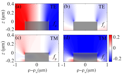
is the visibility of the standing wave; and equality holds when . Here, is a visibility amplitude factor. The presence of the axial field reduces the visibility of the standing wave: vanishes when and is largest with . As shown in Fig. A.2, the visibility of the TE mode is above the microring due to the smallness of the axial component. On the contrary, for TM-mode a smaller above the waveguide results from large as seen in Fig. A.1.
Appendix B AC Stark shift in an evanescent field trap
B.1 Scalar and vector light shifts in the ground state
When a ground state atom is placed above a microring with a strong evanescent field that is far-off resonant from the atomic resonances, it experiences a spatially varying AC stark shift
| (19) |
where is the dynamic polarizability tensor and is the vector components of the microring evanescent field. In the irreducible tensor representation, the above tensor product can be separated into contributions from scalar (rank-0), vector (rank-1), and tensor (rank-2) terms
| (20) |
where
| (21) | ||||
| (22) | ||||
| (23) |
and are the corresponding scalar, vector, and tensor polarizabilities, is the total angular momentum operator, and is the quantum number. We note that, for ground state atoms in the angular momentum state, . Therefore we do not consider throughout the discussions. The calculations of follow those of Ding et al. (2012), using transition data summarized within, and is not repeated here. Table 1 lists the value of polarizabilities used in the trap calculation.
| (a.u.) | (a.u.) | ||
|---|---|---|---|
| 3033 | -1632 | -0.5382 | |
| -2111 | -643.0 | 0.3046 |
B.2 Scalar and vector light shifts in an evanescent field trap
To form an evanescent field trap, the microring must be excited through an external waveguide. Equations (15-16) can be used to calculate the single-end excited resonator electric field. The complex polarization of a mixed resonator mode induces both scalar and vector components of the AC Stark shift. Using from Eq. (16), the scalar light shift forms a standing-wave potential
| (24) |
Meanwhile, the vector light shift depends on the cross product between the CW and CCW components in the excited field
| (25) |
which is smooth along the microring (independent of coordinate) and varies only in the transverse coordinates . Here, is the build up factor for the vector potential
| (26) |
In a special case when the atomic principal axis lies along the -axis, the vector light shift can be explicitly written as
| (27) |
where are the angular momentum ladder operators.
The explicit dependence on angular momentum operators in reveals a diagonal, state-dependent energy shift and off-diagonal coupling terms. Near the anti-nodes of a standing wave Eq. (16), which should serve as trap centers, the ratio between the vector and the scalar light shifts is found to be (dropping -related factors)
| (28) |
where represent the amplitudes of the diagonal and off-diagonal terms in the vector light shift Eq. (27), respectively.
Equation (28) suggests that the state dependent vector light shift can be smaller than the scalar shifts. For far-off-resonant light with frequency that is largely red- or blue-detuned from both cesium D1 and D2 lines, the vector polarizability ; see Table 1. The electric field polarization factor
| (29) |
provides additional suppression. As shown in Fig. B.3, a TE mode supports an off-diagonal factor and the diagonal factor . For a TM mode, and .
B.3 Eliminating the vector light shifts
In practical experiments, a state-independent trap is much preferred since it prevents parasitic effects such as dephasing or trap heating. To fully eliminate the vector shift, a straightforward method is to choose a proper detuning such that (provided that ) and , as suggested by Eqs. (26-27) and illustrated in Fig. B.4 (a). Visibility is at the same time maximized as creates equal superposition of CW and CCW modes up to a relative phase shift, as seen in Eq. 15. The excited field becomes linearly polarized with spatially rotating polarization, similar to the form in Eq. 10, and leads to zero vector shift. In this simple scheme, the scalar light shift build-up factor is also near its maximal value, as in Fig. B.4(a, c).
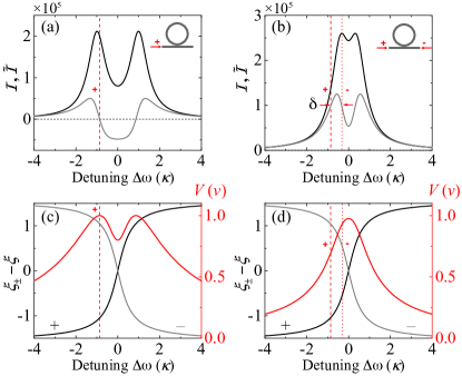
In cases when , a second option is to excite the resonator from both ends of the external waveguide, with one frequency aligned to the resonance peak and another one aligned such that the two excited fields have equal build-up factors as shown in Fig. B.4 (b). Due to large relative frequency detuning between the two fields, their contributions to the vector light shift, Eq. (27), are of opposite signs and can be summed up incoherently to completely cancel each other. The standing wave pattern in the total scalar shift [Eq. (24)], on the other hand, still remains highly visible. For the example shown in Fig. B.4 (b, d), the two excited fields have unequal intensity buil-up factors, , visibilities and a differential standing-wave phase shift . The incoherent sum of the scalar light shifts results in a new visibility
| (30) |
which gives and the standing wave pattern remains sufficiently strong.
B.4 Eliminating standing wave in the scalar potential
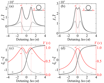
Modifications in the previous schemes allow further elimination of the standing wave potential. We make use of the fact that the standing wave patterns can be created 180 degrees out of phase with respect to each other when we excite the microring from either end of the bus waveguide with exact opposite frequency detuning to the bare resonance , as shown in Fig. B.5 for (a,c) and (b,d). Since we also have equal energy build-up factors and visibilities, , the standing wave pattern as well as the vector light shift can be fully cancelled, allowing us to create a state-independent, smooth evanescent field potential along the microring that is highly useful in our two-color trapping scheme.
Appendix C Losses in microring resonators
C.1 Fundamental limits of the microring platform
Without considering fabrication imperfections, the cooperativity parameter is fundamentally limited by the intrinsic quality factor due to finite material absorption () and the bending loss (). For stoichiometric LPCVD nitride films, it has been estimated that the absorption coefficient dB/m in the near infrared range Ji et al. (2017). At cesium D1 and D2 wavelengths, for example, we estimate that should contribute little to the optical loss in a fabricated microring. On the other hand, we numerically estimate the bending loss from FEM analysis. We have empirically found that when the radius of a microring is beyond 15 micron, as in our case, and the effective refractive index of the resonator mode is , constraining the minimum mode volume to be for an atom trapped around nm ( for a solid state emitter at the waveguide surface). Without further considering fabrication imperfections, the fundamental limit for the cooperativity parameter could be as high as ( on the waveguide surface).
C.2 Surface scattering loss
The analysis of surface scattering loss has been greatly discussed in the literature, see Payne and Lacey (1994); Poulton et al. (2006); Borselli et al. (2005) for example. Here we adopt an analysis similar to Borselli et al. (2005), but with a number of modifications. We evaluate the surface scattering limited quality factor by calculating
| (31) |
where is the energy stored in the ring, and are the unperturbed dielectric function and the resonator mode field, respectively, and is the radiated power due to surface scattering.
We adopt the volume current method Kuznetsov (1985) to calculate the radiation loss. To leading order, the radiation vector potential is generated by a polarization current density created by the dielectric defects, where is the dielectric perturbation function that is non-zero only near the four surfaces of the microring. In the far field, we have
| (32) |
The radiation loss can thus be estimated by the time averaged Poynting vector.
We note that the above method works best for a waveguide embedded in a uniform medium Kuznetsov (1985). In our case, a nitride waveguide on a dioxide substrate embedded in vacuum, an accurate calculation is considerably more complicated due to dielectric discontinuities in the surrounding medium. Here, we neglect multiple reflections and estimate the amount of scattering radiation in the far field (in vacuum) by separately evaluating the contributions from the four surfaces of a microring waveguide. We take , where and are the dielectric constants of nitride and the surrounding dioxide substrate or vacuum, respectively, and represents the distribution function of random irregularities near the -th surface. For the side walls at , surface roughness caused by etching imperfections; for top and bottom surfaces at , this results from imperfect film growth.
Using, Eqs. (32), we could then evaluate
| (33) |
where
| (34) |
The random roughness in the second line of the integral varies at very small length scale , as suggested by our AFM measurements. Thus, the electric field related terms in the first and the second lines above can be considered slow-varying. The integration over large ring surfaces should sample many local patches of irregularities, each weighed by similar electric field value and polarization orientation. We may thus replace with an ensemble averaged two-point correlation function , which can be determined from the AFM measurements. We approximate the two-point correlation with a Gaussian form
| (35) |
for top and bottom surfaces () and, similarly,
| (36) |
for the side walls (). In the above, and are the root-mean-squared roughness and the correlation length, respectively. is the Dirac delta function, and for lying within the range of the (perfect) ring waveguide and otherwise.
Plugging Eq. (35) into Eq. (34) to evaluate loss contribution from top and bottom roughness, we obtain
| (37) |
where, due to the short correlation length , we can simplify the azymuthal part of the integral by taking and arrive at the following
| (38) |
In the above, we used the fact that the integrant is none-vanishing only when and . Here is a geometric radiation parameter due to mode-field polarizations coupled to that of freespace radiation modes Borselli et al. (2005); We note that is polarization independent, different from the result of Borselli et al. (2005), because the surface scatterers are approximately spherically symmetric () in the sense of radiation at farfield.
Plugging Eq. (38) into Eq. (37), we arrive at
| (39) |
where is the averaged mode field and is the effective volume of the scatterers.
For scattering contributions due to side wall roughness, we adopt similar procedures and obtain
| (40) |
where the effective volume is , the effective mode field and . Here, is polarization dependent due to the geometric shape of the side wall roughness, with and .
We note that the apparent difference between the mode field contributions in Eqs. (39) and (40) is due to the effective volume of the surface and side wall scatterers. At the side walls, because the vertical length of the edge roughness is about the thickness of the waveguide and is rather comparable to the wavelength, interference effect manifests and modifies the scattering contribution from the mode field . If , gives the averaged mode field squared at the side walls.
We then evaluate the scattering-loss quality factor as
| (41) | ||||
| (42) |
where and define
| (43) | ||||
| (44) |
as the normalized, weighted mode field energy density.
In the main text we optimize by calculating . From Eq. (42) with given roughness parameters, it is clear that can be made higher by increasing the degree of mode confinement, which requires increasing the cross-section of the microring () to mitigate the surface scattering loss. However, this will be constrained by the desire to decrease the mode volume, that is, to increase the mode field strength at the atomic trap location . Moreover, the radius of the microring cannot be reduced indefinitely because of the increased bending loss and the surface scattering loss at the sidewall (the guided mode shifts toward the outer edge of the microring, as shown in Fig. A.1). An optimized geometry balances the requirement for proper mode confinement and small mode volume to achieve high .