Finite-size effect of critical penetration of Pearl vortices in narrow superconducting flat rings
Abstract
We revisit the critical penetration of Pearl vortices in narrow superconducting flat rings cooled in magnetic fields. Scanning superconducting quantum interference device microscopy measurements showed how magnetic field penetrates and vortices are trapped in flat rings made of amorphous MoGe thin films. Counting the number of trapped vortices for each image, we found that the vortices are completely excluded from the ring annulus when the applied field is below a threshold field : Above this field, the vortices increase linearly with field. The obtained values of depend on the annulus width and follow the relation with the superconducting flux quantum . This relationship provides an insight into the effect of the net-current circulating in the annular region, and also leads to a precise control to trap or eliminate vortices in flat rings.
I Introduction
Recent advances in microfabrication techniques provide an opportunity to manipulate the magnetic flux quantized in units of induced in a variety of superconducting micro/nano structures and devices cooled in magnetic fields. Of particular interest is the arrangement of quantized vortices (called Pearl vorticesPearlAPL1964 ) in thin films of finite size, which has attracted considerable academic interest for last two decades. In addition to the self-energy of the vortex, the vortex-vortex interaction depends on the size and shape of the film.Brandt2005 The interplay between the intervortex interaction and the confinement results in unique vortex states, different from the Abrikosov-vortex lattice in bulk superconductors. These include vortex polygons,Buzdin1993 concentric vortex shells,PalaciosPRL2000 ; BaelusPRB2004 and vortex fusion,MoshNature1995 ; BenoistZphys1997 ; SchweigertPRB1998 ; Chibotaru2004 which have been directly observed in imaging experiments on small superconducting discs,GrigoPRL2006 ; Kokubo2010 squares,MiskoSUST ; Kokubo2014 , triangles,ZhaoEPL2008 ; Kokubo2015 pentagons,HoSUST2013 and others.CrenPRL2009 ; TominagaPRB2013 ; Dang2018
In recent years there has been renewed interest in vortices trapped in small superconductors as one of the control sources for non-equilibrium excess quasiparticles. While micro/nanostructured superconductors have been incorporated in various devices for growing fields such as quantum information processing and metrology, their performances were (partly) degraded by accumulated excess quasiparticles. To suppress the overheating in the devices, vortex-trapped small superconductors can be key elements for tuning the population of the quasiparticles, leading to the improvement of quality factor in superconducting resonators,NsanzinezaPRL2014 the reduction of the energy relaxation time of superconducting qubits,WangNcomm2014 and the suppression of excessive current in electron turnstiles.TaupinNcomms10977 Then, it has become a revisited question how to control the vortex penetration and subsequent vortex trap in small superconductors with various shapes.
The critical penetration of vortices in small superconductors has been discussed through the size dependence of the characteristic threshold field for the complete exclusion of vortices from a thin superconducting stripLikhalev1972 ; Maksimova1998 ; Stan2004 ; KuitPRB2008 or a thin superconducting discBenoistZphys1997 ; Kogan2004 ; NishioPRL2008 where electromagnetic properties are governed by Pearl’s effective penetration depth with magnetic penetration depth and film thickness .PearlAPL1964 In the strip the first vortex trap occurs when magnetic field exceeds ln with being strip width, which is set by the energy balance between the self-energy ln of one vortex trapped in the middle of the strip and the interaction energy of the vortex with the screening current flowing in strip edges.Maksimova1998 The relationship between and has been studied through vortex imaging experiments on Nb, NdBa2Cu3Oy and YBa2Cu3O7-δ thin strips with a few tenth micron widths cooled in magnetic fields up to 1 mT.Stan2004 ; KuitPRB2008 ; SuzukiAPL2000
The issue of the size dependent is not trivial when it comes to a narrow flat ring. In response to applied magnetic field, the ring has the circulating current (e.g. in counterclockwise direction near the inner axial edge) induced by fluxoid with integer ) threading the hole and the screening current (flowing in clockwise direction near the outer axial edge) by applied magnetic field. The superposition of the two currents results in the counter current flow in the annular region between inner and outer radii . This resembles the situation for the strip which carries equal and opposite currents in edges. Therefore, one might expect naively that the threshold field for the complete vortex exclusion from the ring annulus depends on the annulus width .Kogan2004 ; Brandt2004 However, varies non-monotonously with due to transitions from the fluxoid state to , while the field dependence of is monotonous. This gives a stark contrast to the narrow strip, implying that the effect of the net current should be taken into account to determine . The situation is also different from a slitted ring/loop, where the net current is interrupted by a slit and the condition holds.Brandt2004 ; Brandt2005
So far much experimental effort has been devoted to the issue of the vortex (flux) trap in slitted superconducting loops for improving the performance of superconducting quantum interference devices (SQUIDs),SuzukiAPL2000 ; Wordenweber2002 while experiments on a simple narrow ring/loop (with no slit) have been limited.MillPRB2015 In this study, we report the direct observation of Pearl vortices trapped in narrow flat rings of amorphous superconducting films with different sizes by scanning SQUID microscopy (SSM). Different from the previous study made on square loops,Mitsuishi2018 the present data on the flat rings are able to examine the relationship between and without ambiguities arisen from the nonuniform width in loops. Our quantitative analysis shows that a fluxoid state with negligibly small net current gives a significant contribution to the first vortex trap.
II Experimental
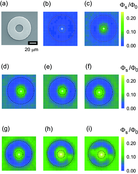
We prepared amorphous MoxGe1-x (MoGe) thin films with 80 2 , which were sputtered in argon gas atmosphere on water-cooled Si (100) substrates from the target composed of high purity germanium pieces (99.999) glued on top of a high purity molybdenum (99.99) plate. The uniformity in molybdenum (or germanium) distribution was confirmed by electron probe microanalysis with JOEL JXA-8530F. The film thickness = 0.21 m was determined by measuring the vertical profile of the sample edge by a stylus surface profiler. Using ultraviolet lithographic and chemical etching techniques, the films were partly patterned into Hall bars to determine the superconducting transition temperature K), the normal resistivity ( 1.4 m at 10 K), and the second critical field . Then, we estimated the zero-temperature magnetic penetration depth 0.46 m and the zero-temperature coherence length 4.4 nm from dirty limit expressions.Kes1983 Because the films are thinner than the penetration depth (), their electromagnetic properties are governed by rather than . The rest of the films were partly patterned into flat rings, as shown in Fig.1a, with different combinations of inner and outer radii for SSM imaging experiments. To reduce possible damage during the scanning, we deposited 0.1 m thick silicon-oxide film on top of the rings. The parameters of five samples we focus in present study are summarized in Table 1. For all the samples, the values of are fixed with 10 m, while those of are changed. This enables us to examine the effect of the annulus width on the critical penetration of Pearl vortices in flat rings.
| m) | m) | m) | T) | |
|---|---|---|---|---|
| C1 | ||||
| C2 | ||||
| C3 | ||||
| C4 | ||||
| C5 |
We used a scanning SQUID microscope (SQM-2000, SII Nanotechnology) with a sensor chip integrating a superconducting pickup coil with the effective diameter of m and niobium-based Josephson junctions. The sensor chip was mounted on a phosphor-bronze cantilever and tilted slightly with respect to the sample stage. By manipulating motorized precision positioning devices assembled under the sample stage, the sample surface was softly in contact with a corner of the sensor chip and scanned in direction during the image acquisition. Due to the weak pinning properties of amorphous MoGe films, the distance between the pickup coil and the sample surface is an important parameter to be controlled as the movement of the pick-up coil can drag and/or kick out vortices during the scanning.Kokubo2010 To reduce the coupled motion of vortices, we kept the distance of 5 m between the pickup coil and the sample surface. This allowed us to image individual vortices in amorphous thin films with reasonable lateral resolutions when the vortex density is low (see the Appendix). Small thermal drift present in the sample stage may distort SSM images and this occurs likely if the large area was scanned with a step size of 1 m. To exclude this drawback in our setup, all the SSM images on rings in the present study were taken with a 4 m step size. The sample stage has a multi-turn wound coil for applying small magnetic field perpendicular to the sample surface. The whole assembly including the sensor chip and the sample stage was covered with a -metal shield. The ambient magnetic field around the sample space was reduced to 1 T, which was subtracted from the magnitude of applied magnetic fields.
III Results and Discussion
Figures 1b-1i show a set of SSM images of the ring sample C4 ( 24.5 m) after cooling to 4.0 0.1 K in applied magnetic fields from 2 to 9 T with 1 T field step. A color bar indicates the magnitude of the magnetic flux through the pickup coil. The flux expulsion observed as a ring allows us to find the position of the sample in each image. One can also find that a dome like magnetic profile appears around the hole center marked with a cross, the intensity of which is larger than that outside the ring. This is known as a result of field focusing into the hole that occurs when small magnetic field (below ) is applied perpendicularly to a flat ring with finite screening.Brandt2004 ; Kirtly2003 There occurs magnetic field penetrations from the inner and outer axial edges (which lead to the counter circulating flow in the annular region), and no isolated magnetic flux is observed in the ring annulus up to 7 T. Meanwhile, as shown in Fig. 1h, one can recognize clearly the sudden appearance of a magnetic flux spot in lower right of the annulus at 8 T. Then, another flux spot emerges in the opposite side of the annulus (see Fig. 1i) at a slightly higher field of 9 T. Subsequently, the number of flux spots increased one by one with magnetic field. Because each spot lies within the annular region, it can be naturally regarded as a Pearl vortex.
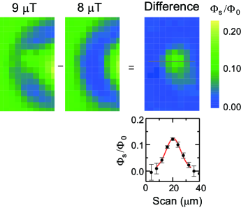
In order to clarify the magnetic flux trapped in the ring annulus, we take the difference between images. An example is shown in Fig. 2 where the part of the image data with the flux spot at 9 T (Fig. 1i) has been subtracted from that at 8 T (Fig. 1h) with the flux-free annular region.subtraction One can see that the magnetic flux trapped in the annulus is clearly visible, while the flux focused in the hole is largely reduced. We plot the profile of magnetic flux intensity along the cross section near the flux center, represented by a solid line (which corresponds to the scan direction of the pickup coil). It shows a broad peak in the annular region. HWHM (Half-width of the half maximum) of the peak is 7 m which is wider than the effective penetration depth (4 K)[= 2.3 m.NishioKPRB2008 This originates from the combined effect of the spread of the magnetic flux at the measurement position apart form the sample surface and the finite size ( 9 m) of the pickup coil. The profile of in Fig. 2 can be qualitatively reproduced by a monopole model because the condition , where and respectively are the in-plain distance and the height of the pickup coil from the flux center, is fulfilled.WynnPRL2001 ; NishioMPRB2008 ; GePRB2013 The magnetic field (perpendicular to the sample surface) originating from the magnetic monopole can be expressed as
As pointed out by Wynn et al.,WynnPRL2001 this model remains still acceptable as a good approximation even at =0, provided that is larger than the effective penetration depth, i.e., . Integrating over the effective area of the pickup coil (assuming a 9 m diameter perfect circle as the pickup coil), we obtain the total flux through the coil as function of . Under the condition of , the best fit to the flux profile (red line in Fig. 2) gives 7.8 0.2, resulting in 0.2 m, which is very close to the actual height of the pickup coil. We note that both width and magnitude of the flux profile are quantitatively close to our previous result of individual Pearl vortices in amorphous MoGe thin films.NishioKPRB2008 Therefore, each flux spot trapped in the ring annulus corresponds to a Pearl vortex accompanying the flux quantum .
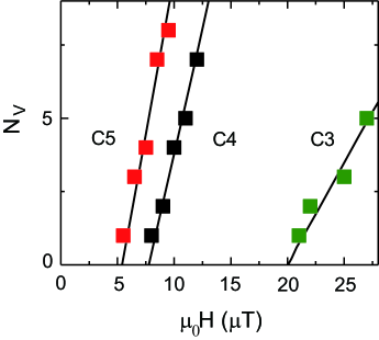
To determine the threshold field for the critical penetration of the C4 ring, we count the number of trapped flux (vortices) in the ring annulus in each image and plot it against applied field in Fig. 3. One can see that for the C4 ring (black symbols) increases linearly with applied field. This behavior can be approximated as with the area 3400 m2 of the annulus. Then, the threshold field 7.8 T is determined by the linear extrapolation to , as in a previous study made on Nb strips.Stan2004 As well as the C4 ring, the linear approximation fits nicely the data obtained in the C5 (C3) ring with wider (narrower) width and results in the lower (higher) threshold field 5.4 (20.2) T (see Fig. 3). Thus obtained values of are listed in Table 1.
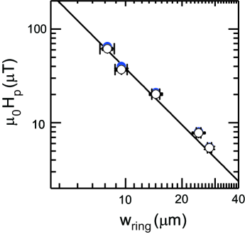
We plot the experimentally obtained values of against in Fig. 4. One can see from this log-log plot that the data follow the relationship of the form , being in good agreement with the naive expectation.Brandt2004 The prefactor was obtained as from the least square fit of the data to the relationship as represented by a solid line. Thus obtained relationship does hold even when using different definitions for (, e.g. the lowest field for one Pearl vortex trapped in the ring annulus), although the prefactor changes slightly.
Let us discuss the prefactor of the relationship by taking into account the net current in the annular region. The first vortex trap in the ring annulus can be sensitively affected by the net force exerted on the vortex. Therefore, it is reasonable to consider the situation for the zero-net current in the ring and incorporate it into the critical penetration. This corresponds to the circularly symmetric situation of with the fluxoid state and may occur when with a characteristic field , which is set by the effective area of the hole.BrojenyPRB2003 ; Brandt2004 Using the above relationship, we obtain
Thus, the prefactor is given by the fluxoid number at multiplied with the ratio of squared annulus width and the effective area. In order to test this conjecture, we quantitatively estimate the fluxoid number and its effective area by following the analysis by Brandt and Clem.Brandt2004 They numerically calculated field and current profiles of a flat ring for arbitrary values of and , covering the shape of our rings studied. For the C4 ring, we find the fluxoid number 4 with the characteristic field 1.8 T and the effective area m2. Here, we use dimensionless factors of and determined respectively from numerical results given in Figs. 6 and 12 of Ref. 30, provided that and 0.29. Substituting these to the above relation, we find that which is close to the experimentally obtained value of . It turns out that the products for the other rings agree with the experimental value within error bars. These reasonable coincidences support the aforementioned conjecture that the critical penetration of Pearl vortices in the ring annulus needs the zero-net-current condition.
We comment on the temperature dependence of the fluxoid number threading the hole. Near the effective penetration depth becomes divergently large (). Thus, one can use the dirty limit expression for the effective area ln.Brandt2004 Using parameters for the C4 ring, we find 5 which is larger than that at 4 K estimated above. This may have an important consequence for the critical penetration in the field-cooled ring, as the excess flux should be excluded from the hole during cooling from to 4 K and can be subsequently trapped as one vortex in the ring annulus at lower temperatures (not close to ). Thus, the temperature dependence of can lead to the reasonable process of the vortex trap in the flat ring cooled at the threshold field.
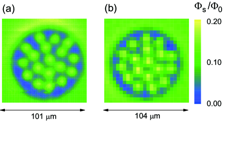
Finally, we discuss the critical penetration of Pearl vortices in narrow square loops. The previous SSM imaging experiments on narrow square loops made of amorphous MoGe and Nb thin films have reported the size dependent threshold field.Mitsuishi2018 The obtained values of obey , where the prefactor is 3.9 when one takes the widest spacing along the diagonal of the square or 1.8 when the narrowest one . These prefactors are also explainable when considering the situation of the zero-net current in loops. Following the aforementioned analysis, together with the numerical results of field and current profiles of a square loop,Brandt2005 we find that 3.7 and 1.4 for the widest and the narrowest spacings of the MoGe-A loop, respectively.parameters These products, together with ones obtained in other loops, turn out to be close to the prefactors in the above relations. Therefore, we believe that narrow flat rings and square loops share the same mechanism of the first vortex trap.
IV Conclusion
To summarize, we have presented SSM images of Pearl vortices trapped in narrow flat rings made of amorphous MoGe superconducting thin films cooled in different magnetic fields. Our data showed clearly the presence of a threshold field , above which the vortices are trapped in the ring annulus and increase linearly with applied field. The experimentally obtained values of depend on the annulus width and obey the relationship of the form with . Quantitative analysis on the prefactor revealed that the critical penetration in a flat ring occurs when the net force exerted on the vortex in the ring annulus becomes negligibly small. These findings are useful for trapping or eliminating Pearl vortices in flat rings, which can be crucial elements for designing various devices for quantum information processing, memory and metrology.
Acknowledgements.
N. K acknowledges M. Mitsuishi for technical assistance. This work was supported by JSPS KAKENHI (Grant Numbers 26287075 and 17K05537), and the Inter-university Cooperative Research Program of the Institute for Materials Research, Tohoku University (Proposal No. 17K0051 and 18K0012).*
Appendix A
The rest of the amorphous MoGe films used in the present study was patterned into other shapes including disks with different diameters. Figure 5a shows a SSM image on a 90 m diameter disk cooled in 8.2 T. The image was taken with a 1 m step size. One can see magnetic flux spots with well spaced (no strong overlaps) and nearly equal magnitude in the disk. They form the triple shell configuration characterized by (1,6,11) which represents that the most inner shell has one (Pearl) vortex, the middle shell is formed by 6 vortices and the most outer shell by 11 vortices.Kokubo2010 Figure 5b shows an image on the same disk cooled slightly higher field of 8.4 T taken with a 4 m step size. Despite large pixel blocks, one can reasonably find how vortices are arranged, supporting that each flux spot observed in Figs. 1h and 1i represents a Pearl vortex even with 4 m step-size measurements. The evolution of quasi-symmetric concentric vortex shells as function of vorticity was obtained from the set of SSM images on the same disk cooled in different magnetic fields.Kokubo2010 This excludes unintended inhomogeneity like cracks in the films used in the present study.
References
- (1) J. Pearl, Appl. Phys. Lett. 5, 65 (1964).
- (2) E. H. Brandt, Phys. Rev. B 72, 024529 (2005).
- (3) A. I. Buzdin, Phys. Rev. B 47, 11416 (1993).
- (4) J. J. Palacios, Phys. Rev. Lett. 84, 1796 (2000).
- (5) B. J. Baelus, L. R. E. Cabral, and F. M. Peeters, Phys. Rev. B 69, 064506 (2004).
- (6) V. V. Moshchalkov, L. Gielen, C. Strunk, R. Jonckheere, X. Qiu, C. V. Haesendonck, and V. Bruynseraede, Nature 373, 319 (1995).
- (7) R. Benoiset, and W. Zwerger, Z. Phys. B 103, 377 (1997).
- (8) V. A. Schweigert, and F. M. Peeters, Phys. Rev. B 57, 13817 (1998).
- (9) L. F. Chibotaru, G. Teniers, A. Ceulemans, and V. V. Moshchalkov, Phys. Rev. B 70, 094505 (2004).
- (10) I. V. Grigorieva, W. Escoffier, J. Richardson, L. Y. Vinnikov, S. Dubonos, and V. Oboznov, Phys. Rev. Lett. 96, 077005 (2006).
- (11) N. Kokubo, S. Okayasu, A. Kanda, and B. Shinozaki, Phys. Rev. B 82, 014501 (2010).
- (12) V. R. Misko, H. J. Zhao, F. M. Peeters, V. Oboznov, S. V. Dubonos, and I. V. Grigorieva, Supercond. Sci. Technol. 22, 034001 (2009).
- (13) N. Kokubo, S. Okayasu, T. Nojima, H. Tamochi, and B. Shinozaki, J. Phys. Soc. Jpn. 83, 083704 (2014).
- (14) H. J. Zhao, V. R. Misko, F. M. Peeters, S. Dubonos, V. Oboznov, and I. V. Grigorieva, Europhys. Lett. 83, 17008 (2008).
- (15) N. Kokubo, H. Miyahara, S. Okayasu, and T. Nojima, J. Phys. Soc. Jpn. 84, 043704 (2015).
- (16) H. T. Huy, M. Kato and T. Ishida, Supercond. Sci. Technol. 26, 06500 (2013).
- (17) T. Cren, D. Fokin, F. Debontridder, V. Dubost, and D. Roditchev, Phys. Rev. Lett. 102, 127005 (2009).
- (18) T. Tominaga, T. Sakamoto, H. Kim, T. Nishio, T. Eguchi, and Y. Hasegawa, Phys. Rev. B 87, 195434 (2013).
- (19) T. D. Vu, H. T. Huy, A. Ito, M. Toji, H. Shishido, M. Kato, M. Hayashi, and T. Ishida, Supercond. Sci. Technol. 31, 125009 (2018).
- (20) I. Nsanzineza, and B. L. T. Plourde, Phys. Rev. Lett. 113, 117002 (2014).
- (21) C. Wang, Y. Y. Gao, I. M. Pop, U. Vool, C. Axline, T. Brecht, R. W. Heeres, L. Frunzio, M. H. Devoret, G. Catelani, L. I. Glazman, and R. J. Schoelkopf, Nature Comm. 5, 5836 (2014).
- (22) M. Taupin, I. M. Khaymovich, M. Meschke, A. S. Mel’nikov, and J. P. Pekola, Nature Comm. 7, 109777 (2016).
- (23) K. K. Likhalev, Sov. Radiophys. 14, 722 (1972) [Radiofizika 14, 919 (1971)].
- (24) G. M. Maksimova, Phys. Solid State 40, 1607 (1998).
- (25) G. Stan, S. B. Field, and J. M. Martinis, Phys. Rev. Lett. 92, 097003 (2004).
- (26) K. H. Kuit, J. R. Kirtley, W. v. d. Veur, C. G. Molenaar, F. J. G. Roesthuis, A. G. P. Troeman, J. R. Clem, H. Hilgenkamp, H. Rogalla, and J. Flokstra, Phys. Rev. B 77, 134504 (2008).
- (27) V. G. Kogan, J. R. Clem, and R. G. Mints, Phys. Rev. B 69, 064516 (2004).
- (28) T. Nishio, A. Toshu, A. Nomura, K. Miyachi, T. Eguchi, H. Sakata, S. Lin, N. Hayashi, N. Nakai, M. Machida, and Y. Hasegawa, Phys. Rev. Lett. 101, 167001 (2008).
- (29) K. Suzuki, Y. Li, U. Utagawa, and K. Tanabe, Appl. Phys. Lett. 76, 3515 (2000).
- (30) E. H. Brandt, and J. R. Clem, Phys. Rev. B 69, 184509 (2004).
- (31) R. Wördenweber, and P. Selders, Physica C 366, 135 (2002).
- (32) S. A. Mills, C. Shen, Z. Xu, and Y. Liu, Phys. Rev. B 92, 144502 (2015).
- (33) M. Mitsuishi, N. Kokubo, K. Kitano, S. Okayasu, T. Nojima, and T. Sasaki, J. Phys.: Conf. Ser. 969, 012074 (2018).
- (34) P. H. Kes, and C. C. Tsuei, Phys. Rev. B 28, 5126 (1983).
- (35) See J. R. Kirtley, C. C. Tsuei, V. G. Kogan, J. R. Clem, H. Raffy, and Z. Z. Li, Phys. Rev. B 68, 214505 (2003) for details in the difference between the magnetic signal at the ring center and that outside the annular ring.
- (36) For the subtraction a careful adjustment was made with respect to sample position in the scale of lateral step size of 4 m.
- (37) T. Nishio, S. Okayasu, J. Suzuki, N. Kokubo, and K. Kadowaki, Phys. Rev. B 77, 052503 (2008).
- (38) J. C. Wynn, D. A. Bonn, B. W. Gardner, Y. J. Lin , R. Liang, W. N. Hardy, J. R. Kirtley, and K. A. Moler, Phys. Rev. Lett. 87, 197002 (2001).
- (39) T. Nishio, Q. Chen, W. Gillijns, K. D. Keyser, K. Vervaeke, and V. V. Moshchalkov, Phys. Rev. B 77, 012502 (2008).
- (40) J. Ge, J. Gutierrez, J. Cuppens, and V. V. Moshchalkov, Phys. Rev. B 88, 174503 (2013).
- (41) A. A. B. Brojeny, and J. R. Clem, Phys. Rev. B 68 174514 (2003).
- (42) We used the fluxoid number and the effective area 1.8 10-10m2 of the centered hole at the penetration field for the MoGe-A square loop with the side length 26 m and the centered hole with the radius 3.5 m.Mitsuishi2018 The effective area was determined from the numerical result given in Fig. 7 of Ref. 2 by using the conditions of and the effective side spacing of the hole.