A nanoscale vacuum-tube diode triggered by few-cycle laser pulses
Abstract
We propose and demonstrate a nanoscale vacuum-tube diode triggered by few-cycle near-infrared laser pulses. It represents an ultrafast electronic device based on light fields, exploiting near-field optical enhancement at surfaces of two metal nanotips. The sharper of the two tips displays a stronger field-enhancement, resulting in larger photoemission yields at its surface. One laser pulse with a peak intensity of W/cm2 triggers photoemission of electrons from the sharper cathode tip, while emission from the blunter anode tip is suppressed by dB to electrons per pulse. Thus, the laser-triggered current between two tips exhibit a rectifying behavior, in analogy to classical vacuum-tube diodes. According to the kinetic energy of the emitted electrons and the distance between tips, the total operation time of this laser-triggered nanoscale diode is estimated to be below 1 ps.
Ultrashort-pulsed lasers are nowadays widely employed to steer electrons on time scales that are orders of magnitude shorter than those of the existing electronics devices Krausz:2014dn ; Schiffrin:2013rc ; Ghimire:2011fk ; Ivanov20133 . For example, photoemission by femtosecond pulsed lasers generates free electrons that are confined within the laser pulse durations. These ultrashort electron pulses have enabled various ultrafast measurements such as time-resolved electron diffraction Siwick21112003 ; Miller07032014 ; Baum02112007 and microscopy Yang24082010 .
It is tempting to utilize these pulsed electrons as carriers in electronic devices because the capability to trigger them by laser pulses bares the potential to overcome the limitations of the operation speed of present electronic devices. The concept of using free electrons as carriers resembles classical vacuum-tube devices, in which electrons emitted via thermionic emission are employed as carriers PrinciplesOfElectronTubes . The functions of the tube devices are achieved via control of the potential of electrodes that determine the trajectories of these electrons, which is readily applicable to control those of the laser triggered electrons as well.
However, replacing the thermal cathode by laser-triggered emission alone is not sufficient to achieve ultrafast electronic devices. This is because the conventional tube electronics exhibit macroscopic (millimeters to centimeters) length scale, and the operation speed of the device is mainly determined by the traveling time of the electrons from one electrode to the other PrinciplesOfElectronTubes . To take advantage of prompt laser-triggered photoemission, a reduction of the electron travel distance is necessary, which leads us to downsize the vacuum-tube devices drastically. Namely, a photoelectron with a typical kinetic energy of eV has a velocity of m/ps in vacuum, and thus the channel distance should be within sub-micrometer length scales to achieve triggering operation faster than 1 THz (i.e., ps).
In this study, we propose a geometry of electronic devices that consist of metal nanotips illuminated by laser pulses. As a first example, we demonstrate a nanoscale vacuum-tube diode consisting of two metal nanotips, which work as cathode (emitting electrons) and anode (capturing electrons).
A key aspect of the metal nanotips is found in the enhancement of the optical near fields at their apexes. These near fields are confined to length scales much smaller than the wavelength of light Novotny-book . They are widely employed to improve spatial resolution in the scanning near-field optical microscopy :/content/aip/journal/jcp/112/18/10.1063/1.481382 and the tip-enhanced Raman spectroscopy Stockle:2000rp . This localized field enhancement also plays an important role in electron emission, resulting in generation of spatiotemporally confined electron pulses PhysRevLett.105.257601 ; Kruger:2011kx ; PhysRevLett.103.257603 ; Herink:2012pi ; Wimmer:2014rw ; Hoffrogge2014 .
One can taylor the strength of the optical near fields by controlling the tip radius: the smaller the tip radius, the larger the field enhancement factor Novotny-book ; doi:10.1021/nl402407r . Due to the stronger field enhancement at the sharper tip, the electron emission yield is much larger there than at the other tip, even if both tips are within the same laser spot. As a result, electrons are mainly emitted from the sharper tip under laser excitation, and this tip consequently works as a cathode. On the other hand, the blunter tip barely emits electrons and receives the electrons emitted from the cathode tip; thus it works as an anode. In this study, we use a comparably blunt tip as anode to take advantage of the well-characterized surface of the tip, as well as to utilize the superior optical access provided by the shape of the tip. Also, the small absorption cross section of a nanotip is advantageous compared with a flat surface.
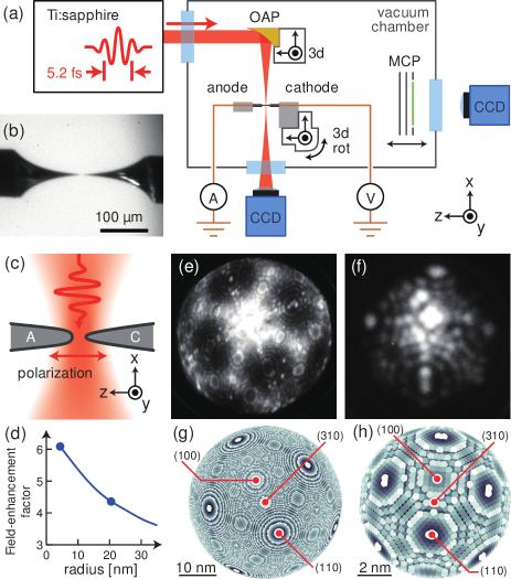
Figure 1(a) shows the schematics of the experimental setup. The cathode and the anode are two tungsten tips that are produced by electro-chemical etching from a single-crystalline tungsten wire in [310] orientation. The tips are placed in an ultrahigh vacuum chamber with a base pressure of Pa. The cathode tip is mounted on a 3d piezo-electric translational stage and faces the fixed anode tip, as shown in the optical microscopic image in Fig. 1(b). After the tips have been approached (described later), they are illuminated by the laser as schematically depicted in Fig. 1(c). We use two-optical-cycle laser pulses from a Ti:Sapphire laser oscillator with a repetition rate of 80 MHz and a center wavelength of 780 nm. The Fourier-transform-limited pulse duration is 5.2 fs (full width at half maximum of the intensity envelope). The dispersion is compensated so that the shortest pulse duration is achieved at the position of the tips, as determined from an interferometric autocorrelation trace. The laser beam is focused on the tips by an off-axis parabolic mirror (OAP), which is mounted on another piezo-electric stage. The laser spot position can be moved by shifting the position of the OAP. The laser spot size has a radius of m. These laser parameters result in a peak intensity of and a peak electric field of at the bare focus in free space for an average power of . The electric field is enhanced around the apex of each tip depending on its radius of curvature, as shown in the simulation results in Fig. 1(d), which are supported by experimental data doi:10.1021/nl402407r . Also, when the two tips are apart further than the tip radii, the near-field enhancement at one tip is not influenced by the presence of the other tip. This condition is always satisfied in this paper.
To measure and control the radii of the two tips, in-situ field ion microscopy (FIM) and evaporation are available PhysRev.102.624 . For this purpose, both tips can be directed to a microchannel-plate electron detector (MCP) independently, which is achieved by placing a rotational stage underneath the 3d translational stage for the cathode tip. FIM with He as an image gas enables us to observe the surface structures of the tips with atomic resolution [Figs. 1(e) and (f). See also the ball-model structures in Figs. 1(g) and (h)]. During the FIM process, a positive voltage (typically 5 kV 15 kV) is applied to obtain an image of the tip apex with the help of field-ionized He ions. By applying a voltage higher ( kV) than the best imaging voltage, the tungsten atoms are field-evaporated. Keeping a tip under this condition, it can be blunted in a controlled manner. An as-grown tip typically has a radius of curvature of nm. In this study, we blunted the anode tip to a radius of curvature of nm, which was determined by counting the number of rings between different crystalline facets Tsong-book . The cathode tip is much sharper, and has a radius of curvature of nm.
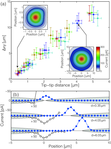
We align the two tips on the same axis and bring them to a distance of nm with the help of the DC-field emission current between the two tips, which depends sensitively on the relative position of the tips. When we scan the position of the cathode tip in a plane perpendicular to the tip axis, the current depends on this position as shown in the insets of Fig. 2(a). We tune the voltage (typically cathode tip at V at a distance of 1 m) so that the maximum current in the 2D map is pA. The data are well fitted assuming that the field strength is inversely proportional to the distance () between them, and that the tunneling current follows the Fowler-Nordheim behavior Fowler:1928 . The tips can be aligned on the tip-tip axis by laterally finding the peak in the current.
After the lateral tip adjustment, a better estimation of the tip-tip distance is made by fitting the width of the lateral () distributions [see Fig.2(a)] as a function of the -position. Although the absolute distance between the tips cannot be directly measured without crashing the two tips, one can approach one tip to the other step-by-step, and the distances between the steps can be determined with an accuracy of nm by the interferometric scale built inside the translational stage. We find a linear scaling between and the tip distance by this step-by-step approach, and extrapolated the position as the position becomes zero. Figure 2(a) shows as a function of the tip distance. Here, the data sets during different approach routines are plotted in the same figure, distinguished by the colors of the data points. For all the data set, the distance between the two tips can be derived with a resolution of nm, without crashing the two tips. Note that the resolution is now limited by the mechanical stability of the experimental system, as we proved experimentally.
Now we focus the laser pulses on the two tips. Figure 2(b) shows the measured current between the laser-triggered cathode and the anode while the laser spot is scanned along their axes. No bias voltage is applied. The two tips are pre-aligned onto a same axis, and for three different tip-tip distances , the laser-position dependence of the current is measured. When the two tips are apart further than the laser spot radii, we measure two peaks with opposite signs in the current as a function of the beam position, corresponding to the emission from the anode and the cathode (bottom in Fig. 2(b)). The emission from the cathode tip is much larger than that of the anode because of the following reasons: Electrons are emitted by absorption of at least three photons of energy eV as the work function of tungsten is 4.35 eV at the W(310) facet Kawano:2008rm . The dominating part of photocurrent is due to three- and four-photon photoemission, without a bias voltage. Hence, the effect of the larger field enhancement factor of the sharper tip is accentuated by the nonlinear nature of the emission process. This explains why the emission current from the sharper cathode tip is times larger than that of the blunter anode tip.
By approaching the two tips ( nm, topmost plot in Fig. 2(b)) within the beam spot (radius 2.3 m), the weaker emission from the anode is submerged by the stronger emission from the cathode. A pair of tips under this condition is expected to work as a diode because electrons should be mainly emitted from the cathode.
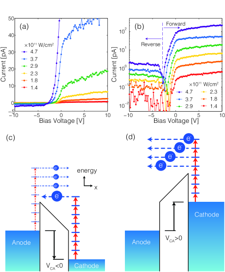
Figure 3 shows the operation of this laser-triggered diode. Figures 3(a) and (b) show the measured current between the laser-triggered cathode and the anode tips as a function of the bias voltage between them. It depends nonlinearly on the bias voltage and shows a rectifying behavior. The forward saturation current is 210 pA for the largest laser intensity ( W/cm2 nominal laser intensity in the bare focus, i.e. without field enhancement). The repetition rate of the laser is 80 MHz, and thus this corresponds to electrons per pulse on average. On the other hand, the reverse saturation current is 2.0 pA, which is two orders of magnitude smaller than the forward one.
The mechanism of diode operation is explained using the energy diagrams depicted in Figs. 3(c) and (d). Electrons are emitted through multi-photon photoemission. When a reverse bias is applied [Fig. 3(c)], the current is reduced because only electrons having higher energies than the potential barrier can reach the anode. The weak current in strong reverse bias conditions results from the weak emission from the anode tip. On the other hand, a forward bias allows all the electrons that overcome the work function to flow [Fig. 3(d)]. The short-circuit current increases as the laser intensity increases.
When a reverse bias is applied, only electrons with higher energy than the bias potential can reach the anode. This determines the lowest initial velocity and thus the longest traveling time of electrons that contribute to the current. Assuming a plate-capacitor potential, a tip-tip distance of nm and V, a conservative estimate yields fs. The photoemission process takes place on the time scale of the laser pulse duration ( fs), thus the whole process including the electron emission and current flow between two electrodes completes on sub-picosecond timescales. In the forward-biased condition, one can reduce the traveling time below by acceleration due to the forward field, which is not limited by the initial kinetic energy unlike the case of reverse-biased condition.
Note that electrons are directionally emitted along the axis of the tip (i.e., the [310] crystalline axis in this work) because the (310) facet of tungsten has the lowest work function PhysRevLett.103.257603 . With a typical opening angle of the (310) electron beam of 10 degrees, the spread in longitudinal velocity caused by this small angular distribution is 1 percent, which is not significant. We also numerically estimated the effect of Coulomb repulsion by using a charged-particle-dynamics simulator (General Particle Tracer) as one electron bunch contains 16 electrons per laser pulse at maximum. For this estimation, the key factor is the initial volume of the bunch. Namely, the emission area is restricted by the radius of cathode tip ( nm), and emission is confined temporally within the laser pulse duration, leading to an initial bunch length of nm. For such a small initial volume, the Coulomb repulsion between electrons occurs significantly only within 10 fs after emission, expanding the electron cloud to 25 nm in radius. After this initial space-charge expansion, the electrons behave almost independently. Therefore, we can neglect corrections by the space-charge effect to the above value of fs as estimated on the basis of the final kinetic energy.
To summarize, we observed rectifying behavior between two metal nanotips, where the electrons are emitted from the cathode tip through multi-photon photoemission by few-cycle laser pulses. The photoemission properties of the two tips were controlled by tuning the tip-radii. This diode device is switched by the laser pulse and operates on sub-picosecond timescales, owing to the short duration of the electron emission process, the comparably high initial kinetic energy of the emitted electrons, and the sub-micron distance between the two electrodes. Reducing the tip-tip distance will allow entering further important regimes for electrons and light fields to interact: when the tip-tip distance is smaller than the near-field decay length, i.e., the radii of curvature of the tips, the optical near fields around the tips are not independent any more and to exhibit stronger field enhancement. Moreover, when the tip-tip distance is within the decay length of the electron’s wave functions, i.e., sub-nanometer length scales, quantum tunneling channels are formed Savage:2012dk . These tunneling channels can be steered by the electric field of light, as expected from the observations that electron emission from nanotips depends on the carrier-envelope phase of few-cycle laser pulses Kruger:2011kx . Together with these advanced methods, our achievement of diode operation with metal nanotips has the potential to operate on attosecond timescales, which could open a way to petahertz electronics operating at optical frequencies.
The authors acknowledge M. Krüger and M. Förster for their technical support, as well as thank S. Thomas for providing the field-enhancement simulation results. This work was supported by the DFG Cluster of Excellence Munich-Centre for Advanced Photonics and the ERC grant “Near Field Atto.” TH acknowledges a JSPS fellowship for research abroad. PD acknowledges a Marie Curie Fellowship (”UPNEX”, project number 302657).
References
- (1) F. Krausz and M. I. Stockman, Nat. Photon. 8, 205 (2014).
- (2) A. Schiffrin, T. Paasch-Colberg, N. Karpowicz, V. Apalkov, D. Gerster, S. Muhlbrandt, M. Korbman, J. Reichert, M. Schultze, S. Holzner, J. V. Barth, R. Kienberger, R. Ernstorfer, V. S. Yakovlev, M. I. Stockman, and F. Krausz, Nature 493, 70 (2013).
- (3) S. Ghimire, A. D. DiChiara, E. Sistrunk, P. Agostini, L. F. DiMauro, and D. A. Reis, Nat. Phys. 7, 138 (2011).
- (4) M. Ivanov and O. Smirnova, Chem. Phys. 414, 3 (2013).
- (5) B. J. Siwick, J. R. Dwyer, R. E. Jordan, and R. J. D. Miller, Science 302, 1382 (2003).
- (6) R. J. D. Miller, Science 343, 1108 (2014).
- (7) P. Baum, D.-S. Yang, and A. H. Zewail, Science 318, 788 (2007).
- (8) D.-S. Yang, O. F. Mohammed, and A. H. Zewail, Proc. Natl. Acad. Sci. 107, 14993 (2010).
- (9) H. J. Reich, Principles of Electron Tubes (McGraw-Hill, New York, 1941).
- (10) L. Novotny and B. Hecht, Principles of Nano-Optics, 2nd ed. (Cambridge Univerisity Press, Cambridge, 2012).
- (11) B. Hecht, B. Sick, U. P. Wild, V. Deckert, R. Zenobi, O. J. F. Martin, and D. W. Pohl, J. Chem. Phys. 112, 7761 (2000).
- (12) R. M. Stöckle, Y. D. Suh, V. Deckert, and R. Zenobi, Chem. Phys. Lett. 318, 131 (2000).
- (13) M. Schenk, M. Krüger, and P. Hommelhoff, Phys. Rev. Lett. 105, 257601 (2010).
- (14) M. Krüger, M. Schenk, and P. Hommelhoff, Nature 475, 78 (2011).
- (15) H. Yanagisawa, C. Hafner, P. Doná, M. Klöckner, D. Leuenberger, T. Greber, M. Hengsberger, and J. Osterwalder, Phys. Rev. Lett. 103, 257603 (2009).
- (16) G. Herink, D. R. Solli, M. Gulde, and C. Ropers, Nature 483, 190 (2012).
- (17) L. Wimmer, G. Herink, D. R. Solli, S. V. Yalunin, K. E. Echternkamp, and C. Ropers, Nat. Phys. 10, 432 (2014).
- (18) J. Hoffrogge, J. Paul Stein, M. Krüger, M. Förster, J. Hammer, D. Ehberger, P. Baum, and P. Hommelhoff, Journal of Applied Physics 115, 094506 (2014).
- (19) S. Thomas, M. Krüger, M. Förster, M. Schenk, and P. Hommelhoff, Nano Letters 13, 4790 (2013).
- (20) E. W. Müller and K. Bahadur, Phys. Rev. 102, 624 (1956).
- (21) T. T. Tsong, Atom-probe field ion microscopy (Cambridge University Press, Cambridge, 1990).
- (22) R. H. Fowler and L. Nordheim, Proc. R. Soc. Lond. A 119, 173 (1928).
- (23) H. Kawano, Prog. Surf. Sci. 83, 1 (2008).
- (24) K. J. Savage, M. M. Hawkeye, R. Esteban, A. G. Borisov, J. Aizpurua, and J. J. Baumberg, Nature 491, 574 (2012).