Magnetic field mixing and splitting of bright and dark excitons in monolayer MoSe2
Abstract
Monolayers of semiconducting transition metal dichalcogenides (TMDCs) with unique spin-valley contrasting properties and remarkably strong excitonic effects continue to be a subject of intense research interests. These model 2D semiconductors feature two fundamental intravalley excitons species - optically accessible ’ bright’ excitons with anti-parallel spins and optically inactive ’dark’ excitons with parallel spins. For applications exploiting radiative recombination of bright excitons or long lifetime dark excitons, it is essential to understand the radiative character of the exciton ground state and establish the energy separation between the lowest energy bright and dark excitons. Here, we report a direct spectroscopic measure of dark excitons in monolayer MoSe2 encapsulated in hexagonal boron nitride. By applying strong in-plane magnetic field, we induce mixing and splitting of bright and dark exciton branches, which enables an accurate spectroscopic determination of their energies. We confirm the bright character of the exciton ground state separated by a 1.5 meV gap from the higher energy dark exciton state, much smaller compared to the previous theoretical expectations. These findings provide critical information for further improvement of the accurate theoretical description of TMDCs electronic structure.
NHMFL] National High Magnetic Field Laboratory, Tallahassee, FL 32310, USA \alsoaffiliation[FSU] Physics Department, Florida State University, Tallahassee, FL 32306, USA Columbia] Department of Mechanical Engineering, Columbia University, New York, NY 10027, USA RPI] Department of Chemical and Biological Engineering, Rensselaer Polytechnic Institute, Troy, NY 12180, USA Rochester1] Department of Electrical and Computer Engineering, University of Rochester, Rochester, New York 14627, USA NHMFL] National High Magnetic Field Laboratory, Tallahassee, FL 32310, USA NHMFL] National High Magnetic Field Laboratory, Tallahassee, FL 32310, USA \alsoaffiliation[FSU] Physics Department, Florida State University, Tallahassee, FL 32306, USA GaTech] School of Physics, Georgia Institute of Technology, Atlanta, GA 30332, USA RPI] Department of Chemical and Biological Engineering, Rensselaer Polytechnic Institute, Troy, NY 12180, USA RPI] Department of Chemical and Biological Engineering, Rensselaer Polytechnic Institute, Troy, NY 12180, USA Columbia] Department of Mechanical Engineering, Columbia University, New York, NY 10027, USA Rochester1] Department of Electrical and Computer Engineering, University of Rochester, Rochester, New York 14627, USA \alsoaffiliation[Rochester2] Department of Physics and Astronomy, University of Rochester, Rochester, New York 14627, USA NHMFL] National High Magnetic Field Laboratory, Tallahassee, FL 32310, USA
![[Uncaptioned image]](/html/1905.10439/assets/Fig00.png)
Transition metal dichalcogenides (TMDCs) with the chemical formula MX2, where M is a group IV-VII transition metal and X is a chalcogen atom (S, Se, Te), have recently emerged as a new class of layered materials that can be exfoliated down to atomically thin layers. Among these materials, the group VI (Mo, W) TMDC monolayers stand out due to their peculiar spin-valley coupled band structure with spin-polarized conduction and valence band states located at the band edges at the corners of the hexagonal Brillouin zone (K+ and K- valleys) with a direct gap in the visible or near-infrared region 3, 1, 2. Because of time reversal symmetry, the sign of the spin splitting is opposite in K+ and K- valley. This allows one to address the spin-valley degree of freedom with either left or right circularly polarized light 4, 5 and, together with the strong excitonic effects 6, create a unique platform to study both light-matter interactions and spin-valley physics in the real two-dimensional (2D) limit.
Since allowed interband optical transitions must conserve the spin and the momentum, the optically active or bright exciton involves an electron and a hole belonging to the same valley but with opposite spins (the spin of the hole is opposite to that of the electron residing in the same valence band). Radiative recombination of intarvalley excitons with the electron and hole constituents with same spins is forbidden and such exciton states are called dark. The understanding of the interplay between low energy bright and dark exciton states is of particular importance since these states ultimately define the radiative properties of 2D TMDCs and their relevance for applications in optoelectronics and valleytronics. In WSe2 and WS2 monolayers, the dark character of the ground state exciton and the energy separation between dark and higher energy bright excitons are firmly established both experimentally and theoretically 7, 8, 9, 10, 11, 12, 13. Meanwhile, the low energy dark excitons in Mo-based compounds have not been probed experimentally so far, and recent theoretical studies have not always been consistent in predicting whether Mo-based TMDCs host dark or bright lowest energy excitons 14, 15, 16, 17, 18.
In this letter, we present the first measurement of the dark exciton in monolayer MoSe2. The main obstacles to detecting dark excitons in MoSe2 are the very close separation between the bright and the higher energy dark states and the low population of the dark exciton states 9. Due to recent progress in the fabrication of high quality BN encapsulated TMDC monolayers, it has become possible to prepare TMDC monolayers with very narrow exciton lines of about 1 meV FWHM 19. With the aid of a strong in-plane magnetic field, we mix bright and dark exciton states, brighten dark excitons, induce further separation of bright and dark exciton states and successfully detect the elusive dark excitons in photoluminescence (PL) and reflectance contrast (RC) spectra. These experimental results provide an unambiguous evidence of the bright nature of exciton ground state in MoSe2 as well as the accurate measure of the energy splitting between the lowest energy bright and dark excitons.
Within a simple single particle picture, the radiative character, dark or bright, of intravalley excitons in monolayer TMDCs depends on the ordering of the spin-up and spin-down conduction sub-bands, CB and CB, separated by a relatively small single-particle gap of the order of tens of meV 20. For the valence states, only the higher energy spin-subband VB needs to be considered because of the large, hundreds of meV, spin splitting in the valence band 21. The relative ordering of lowest energy conduction subbands in MX2 monolayers, which are formed mostly by orbitals of transition metal atoms 22, is different for Mo- and W-based TMDCs. In molybdenum compounds, the lowest conduction band and the the highest valence band share the same spin projection, so the lowest energy exciton state is expected to be optically active. However, the actual energy separation between the lowest energy bright and dark excitons states, , has additional contributions from the short-range electron-hole exchange interaction as well as enhanced binding energy of dark excitons due to their heavier mass compared with bright excitons (see the theory section in the Supporting Information) 16, 17.
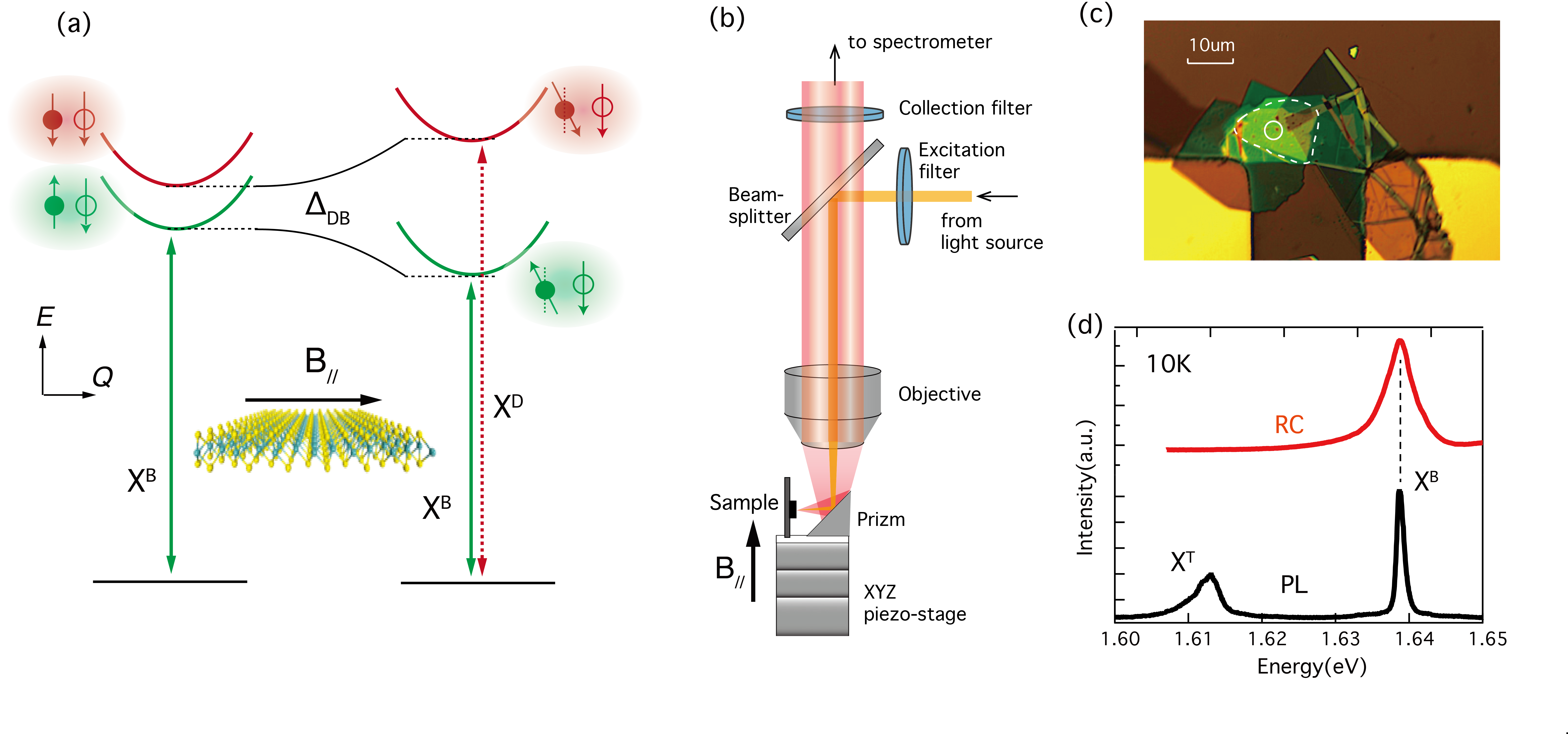
In order to access the dark exciton states, we apply an in-plane magnetic field (,) to separate more dark () and bright () excitons and brighten otherwise unaccessible dark excitons. This is illustrated in Fig.1a where we show a cartoon of the dispersion relation of excitons as a function of the exciton center-of-mass wavevector (). Only excitons located within the photon dispersion cone are allowed to recombine radiatively. The in-plane magnetic field does not couple to the orbital motion of the electrons and can effectively perturb the spin magnetic momenta of band electrons only. The effect of B// on the spin orientation of valence band electrons is negligible because of the large separation of spin-orbit split valence bands. Thus, the system can be approximated by a two-level Hamiltonian for bright and dark exciton states (see the theory section in the Supporting Information):
 \captionsetup
justification=justified, singlelinecheck=false
| (1) |
where and refer to the energies of the bright and dark states at zero magnetic field, the off-diagonal terms introduce their field-induced coupling, gcb is the in-plane conduction band -factor and is the Bohr magneton. shifts the energies of bright and dark excitons in opposite directions:
| (2) |
where the plus /minus sign applies to the bright/dark exciton branches. also provides small but finite optical oscillator strength, proportional to , for dark excitons.
Magnetic brightening of dark excitons has been observed in tungsten-based TMDCs 7, 10, where the gap between bright and dark excitons is relatively large, 50 meV. However, the actual field induced splitting between the bright and dark excitons has not been detected. From Eq. 2 we expect the change of exciton energies at the highest applied magnetic fields (31 T) to only be about (55-75) eV for WS2 or WSe2, almost impossible to detect by standard methods. In contrast, since the field induced splitting is inversely proportional to the zero-field (in the weak-field approximation), it is expected to be much stronger in MoSe2, eventually reaching the meV scale at 20-30 T.
Fabricating high quality MoSe2 monolayers with narrow PL linewidth of about a 1 meV is a crucial factor for detecting the exciton fine structure. Our samples were prepared by mechanical exfoliation of CVT or flux grown bulk MoSe2 single crystals, then transferred and encapsulated in hexagonal boron nitride (hBN). A piece of few-layer graphene was used as the contact electrode of the single layer MoSe2 and another piece was used as the transparent top-gate electrode on the top layer BN. The typical size of the monolayer MoSe2 is about 10 10 (Fig.1c). Our hBN encapsulated samples exhibit very narrow exciton emission PL peaks (with FWHM as low as 1.1 meV at 10 K ) approaching the intrinsic limit 19.
Low temperature magneto-spectroscopy measurements were carried out in the Voigt geometry (light wavevector perpendicular to ) with custom micro-spectroscopy setups equipped with a nonmagnetic objective and a three-axis piezostage for fine in-situ positioning as illustrated in Fig. 1b. The PL measurements were performed with a 31 T resistive magnet using excitation by a continuous-wave laser with a photon energy 2.41 eV (514 nm wavelength). To measure the reflectance contrast (RC), , we employed a similar setup coupled to a 17.5 T superconducting magnet and used a Hg arc lamp with a combination of appropriate bandpath filters to define the spectral region of interest. The excitation light was focused by an objective (NA=0.5) to a spot size of 2 m. The excitation power delivered to the sample was 1 W or less to avoid sample heating and minimize light-induced doping. The PL emission or reflected light was collected by the same objective and detected by a spectrometer equipped with a TE cooled CCD camera. The presented spectra were collected at 10 K and recorded with a spectral resolution of 0.11 meV. Characteristic zero field spectra of the monolayer MoSe2 are shown Fig.1d. In accordance with prior studies, we observe strong and narrow PL emission line for neutral bright exciton (XB) at 1.6388 eV and PL signal from charged excitons or trions (XT) at 1.613 eV. The RC spectrum shows only one pronounced peak associated with XB.
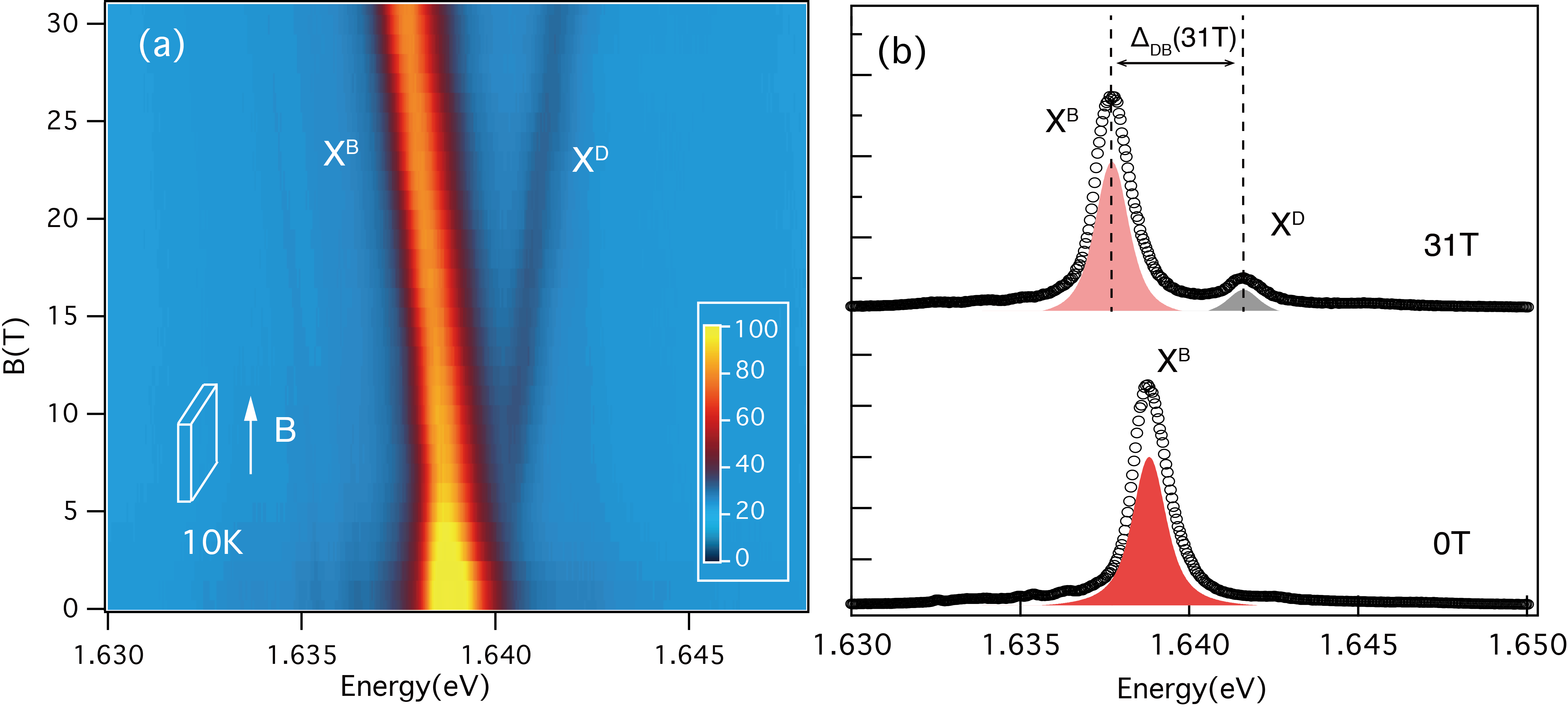
To show the effect of the in-plane magnetic field on exciton emission, we plot in Fig.2a the 2D color map of PL intensity as a function of magnetic field from 0 T to 31 T. As increases, the XB is redshifted and an additional peak, labelled as XD, emerges on the higher energy of XB side exhibiting a blueshift. At the highest magnetic field of 31 T, XB shifts by 1.1 meV and the separation between two peaks, XB and XD, reaches approximately 4 meV. It is instructive to note that these observations provide an explanation for the results from our earlier attempts to detect field induced bright-dark excitons splitting in the PL spectra from MoSe2 monolayers on SiO2/Si substrates. Because the exciton PL line was relatively broad, FWHM=7.3 meV, the spitting could not be resolved spectroscopically even at =31 T. However, as illustrated in Supplementary Fig. S1, the field dependent behavior of the exciton PL peak measured on Si/SiO2 MoSe2 (0.8 meV red shift and 3 meV broadening) agrees well with the the actual splitting of the bright and dark exciton resolved in PL and RC spectra from hBN encapsulated MoSe2.
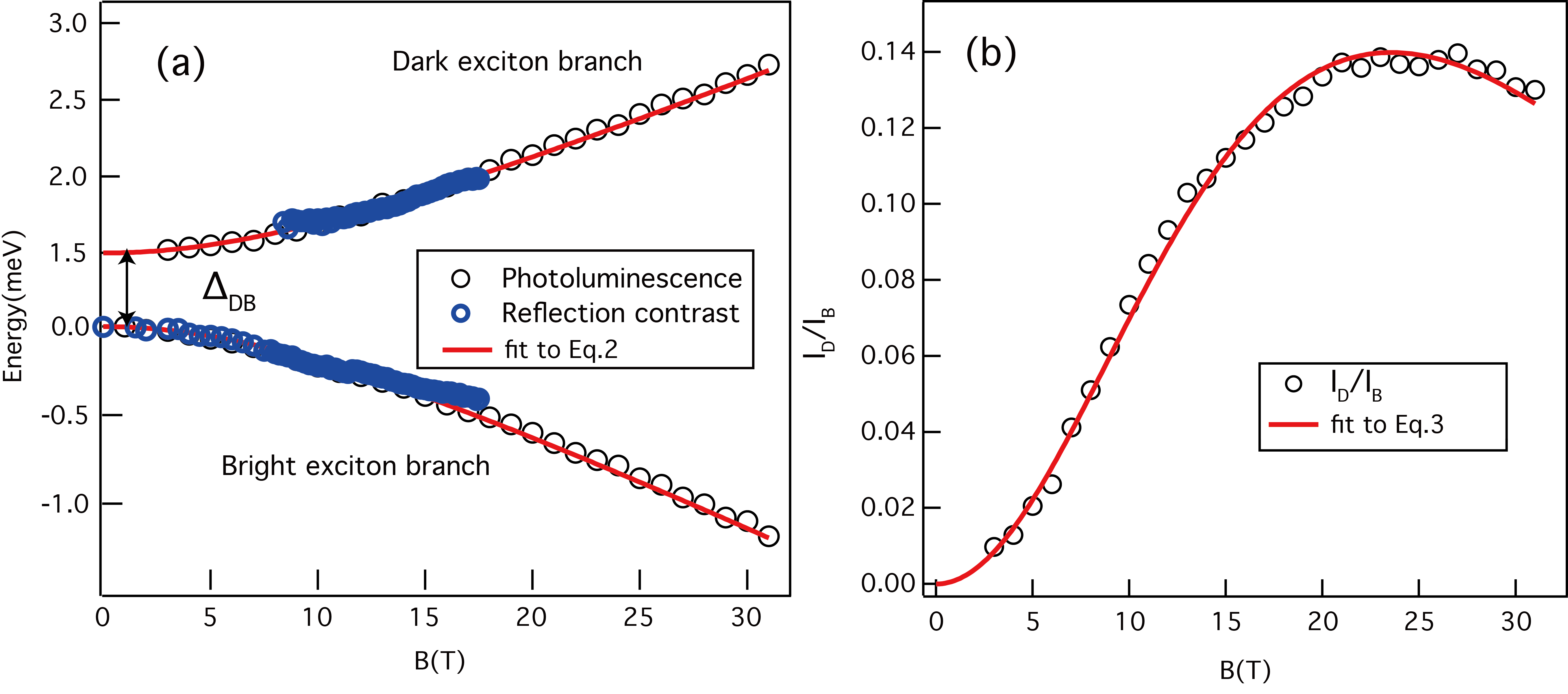
Since the observed behavior reflects very well the anticipated brightening of the dark exciton and field induced energy shift of bright and dark excitons in opposite directions, the emerging high energy peak is attributed to the magnetically brightened dark exciton. For a quantitative analysis of PL evolution with , we use a pseudo-Voigt line shape to fit the spectra. The resulting overall change of XB and XD energies is plotted in Fig.3a. To ensure the reliability and consistency of the experiment and analysis, we also plot the exciton energies extracted from the RC spectra measured in fields up to 17.5 T (detailed comparison of PL and RC spectra is presented in Supplementary Fig.S1). Both data sets consistently overlap, ensuring the validity of the PL results at higher magnetic fields.
 \captionsetup
justification=justified, singlelinecheck=false
As expected from the two band model, the energy of the bright (dark) exciton first exhibits a quadratic increase (decrease) followed by a linear dependence in the high field limit. Despite its simplicity, the model provides a facile means for accurate measure of the dark exciton energy at zero magnetic field and the -factor. By fitting the measured and (see Fig.3a) we extract a g-factor of 2.0 0.1. This confirms the assumption that acts through mixing spins of the conduction band electrons, and the orbital or valence band contributions are negligible. For the zero-field dark exciton, we obtain =1.6403 eV, which places it above the bright state by just =1.5 meV. This result represents the first unequivocal experimental observation of dark excitons in monolayer MoSe2 and provides a clear evidence that the exciton ground state in this system is optically bright.
The energy splitting between the bright and dark excitons at the light cone, , has contributions from spin-orbit coupling energy splitting of the conduction band (), short range electron-hole exchange (), and the fact that dark and bright excitons have different masses and therefore different binding energies (). To compare the experimental value of with theory, one has to accurately calculate the values of , and . To date, such a comparison is ineffective because the variation in reported ab-initio calculations of these parameters is often larger than 10 meV 16, 23, 17, 7, i.e. larger than our measured value of in monolayer MoSe2. Nonetheless, we can still make few consistent observations. Firstly, we note that due to the repulsive nature of the short-range exchange 16, 17, 7, and because dark excitons are heavier than bright ones (dark excitons involve the conduction band with heavier effective mass). Accordingly, to offset the negative value contributions of , the value of should be positive in monolayer MoSe2 in order to yield meV. Similarly, assuming that has similar magnitude in Mo- and W-based compounds, the value of should be negative in WSe2 and WS2 monolayers in order to yield meV and meV, respectively 9. Next, following the procedure described in the Supporting Information, we evaluate the binding energies of bright and dark excitons and obtain meV in MoSe2 and -16 meV in WSe2. Assuming meV 16, 7, we can further infer that is in the ballpark of meV in monolayer MoSe2 and meV in monolayer WSe2. The latter is consistent with the measured value reported in Ref. 7. We note that in addition to the contribution from spin-orbit coupling, the value of is affected from band-gap renormalization in electron-doped samples due to many-body exchange interactions 24, 25. The experimental results and the analysis we have provided in this paper deal with intrinsic (un-doped) monolayers.
 \captionsetup
justification=justified, singlelinecheck=false
We now discuss the relative intensities of the PL emission of dark and bright excitons, that we plot as a function of in Fig.3b. At low magnetic fields, the dark exciton emission grows quadratically with , which is in agreement with the predictions of the two-band model, , and previous observations in W-based monolayer TMDCs 7, 10, 13. However, we find that in MoSe2, the ratio of PL intensities deviates from the simple quadratic dependence at magnetic fields above 7-10 T, saturates at higher fields and starts decreasing above 25 T (Fig.3b). To understand this behavior, we have to consider changes in the thermal population of . Since the bright exciton is the ground excitonic state and the separation between bright and dark states increases with , the population of the high-lying dark state becomes thermally suppressed as magnetic field increases. Assuming thermal equilibrium occupation numbers, we modify the expression for the relative intensity by adding a Boltzmann factor:
| (3) |
which results in excellent fit to the experimental data (Fig.3b).
justification=justified, singlelinecheck=false
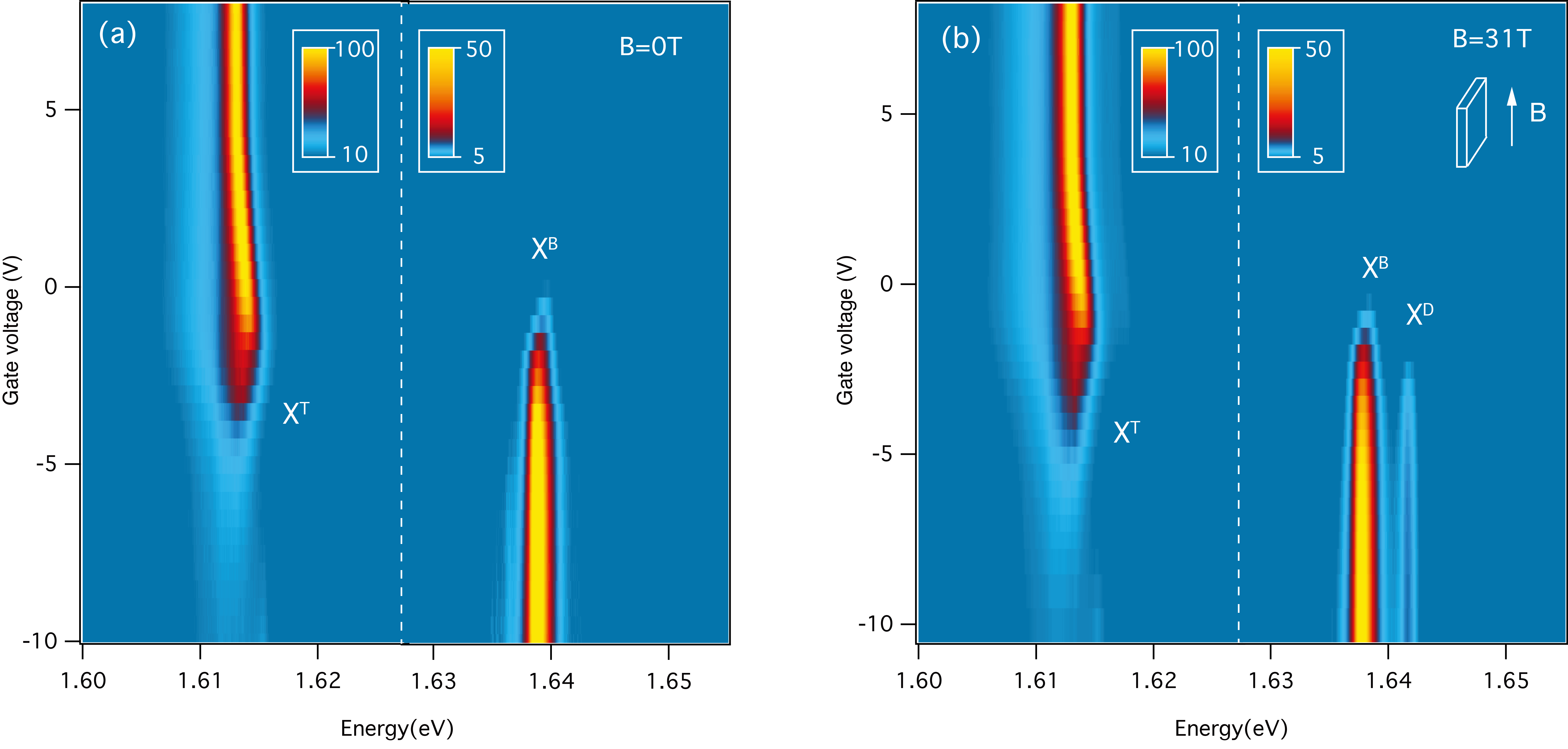
Finally, we briefly discuss another possible mechanism, the Bychkov-Rashba effect 26, that may flip the spin of the conduction band electrons and contribute to brightening of the dark exciton. The Bychkov-Rashba type coupling between dark and bright intraband excitons would require breaking the mirror symmetry in respect to the monolayer plane, which could be induced, for example, by out-of-plane electric field generated by a gate or by unintentional, impurity related charge of the substrate 15, 27. To examine this possibility, we perform gate dependent PL measurements. Figure 4a shows a color map of the PL spectrum of the device at zero magnetic field as a function of the top gate voltage. In the whole wide range of applied gate voltages, only two PL peaks are observed related to neutral bright exciton emission () and charged exciton emission (). No signatures of the PL emission on the higher energy side of can be detected in the spectra acquired at 0 T. The gate dependent PL measured at 31 T (Fig.4b) clearly reveals a signal associated with the emission from dark excitons, , situated at approximately 4 meV above . The energy separation and relative intensities are nearly independent on the gate voltage, and, consistent with theoretical estimations, indicates that the electric field does not contribute to the brightening of dark excitons. Even at relatively high electric field of 1 V/nm, the resulting radiative rate for dark excitons is expected to be four orders of magnitude smaller compared to the effect of of an applied in-plane magnetic field of 30 T 27. The negligible role of the Rashba-induced mixing between dark and bright excitons in our experiment is corroborated by the fact that this interaction is proportional to the exciton wavevector (see the Supporting Information), and therefore its effect vanishes within the light cone wherein .
In conclusion, we have observed magnetic field induced brightening of the dark exciton and splitting of bright and dark neutral excitons in high quality monolayer h-BN encapsulated MoSe2.
The superior sample quality and the use of a strong in-plane magnetic field enable a direct spectroscopic probe of dark excitons.
We have confirmed that the lowest energy exciton state is optically active. The energy separation between the ground state bright exciton and higher energy dark exciton is determined to be 1.5 meV.
This result implies that the energy splitting in the conduction band is a few tens of meV in order to offset the reduced binding energy of bright excitons due to the repulsive short-range electron-hole exchange as well as their lighter mass compared with dark excitons. Importantly, our findings demonstrate that the bright and dark exciton branches are nearly degenerate, and this result may be intimately related to the enhanced valley depolarization in monolayer MoSe2 28, 29, 30.
ACKNOWLEDGEMENTS.
This work was primarily supported by the Department of Energy, Basic Energy Sciences, under Contract No. DE- FG02-07ER46451.
The MoSe2 crystal growth and the sample fabrication at Columbia University were supported by
by the NSF MRSEC program through Columbia in the Center for Precision Assembly of Superstratic and Superatomic Solids (DMR-1420634).
The device fabrication at Rensselaer Polytechnic Institute (RPI) was supported by the NY State Empire State Development’s Division of Science, Technology, and Innovation (NYSTAR) through Focus Center-NY RPI Contract C150117. S.-F. Shi acknowledges support by AFOSR through Grant FA9550-18-1-0312.
The experiments were performed at the National High Magnetic Field Laboratory (NHMFL), which is supported by NSF Cooperative Agreement DMR-1157490, DMR-1644779 and the State of Florida.
The work at the University of Rochester was supported by the Department of Energy, Basic Energy Sciences, under Contract No. DE-SC0014349.
References
- 1 Mak, K. F., Lee, C., Hone, J., Shan, J. & Heinz, T. F. Atomically Thin MoS2: A New Direct-Gap Semiconductor. Phys. Rev. Lett. 105, 136805 (2010)
- 2 Splendiani, A. et al. Emerging Photoluminescence in Monolayer MoS2. Nano Lett. 10, 1271 (2010)
- 3 Xiao, D., Liu, G.-B., Feng, W., Xu, X. & Yao, W. Coupled Spin and Valley Physics in Monolayers of MoS2 and Other Group-VI Dichalcogenides. Phys. Rev. Lett. 108, 196802 (2012)
- 4 Mak, K. F., He, K., Shan, J. & Heinz, T. F. Control of valley polarization in monolayer MoS2 by optical helicity. Nature Nanotechnol. 7, 494 (2012).
- 5 Cao, T. et al. Valley-selective circular dichroism of monolayer molybdenum disulphide. Nature Communications 3, 887 (2012).
- 6 Yu, H., Cui, X., Xu, X. & Yao, W. Valley excitons in two-dimensional semiconductors. National Science Review 2, 57 (2015)
- 7 Zhang, X.-X. et al. Magnetic brightening and control of dark excitons in monolayer WSe2. Nat Nano 12, 883 (2017)
- 8 Zhou, Y. et al. Probing dark excitons in atomically thin semiconductors via near-field coupling to surface plasmon polaritons. Nat Nano 12, 856 (2017).
- 9 Wang, G. et al. In-Plane Propagation of Light in Transition Metal Dichalcogenide Monolayers: Optical Selection Rules. Phys. Rev. Lett. 119, 047401 (2017)
- 10 Molas, M. R. et al. Brightening of dark excitons in monolayers of semiconducting transition metal dichalcogenides. 2D Mater. 4, 021003 (2017)
- 11 Vasconcelos, R., Braganca, H., Qu, F. & Fu, J. Dark exciton brightening and its engaged valley dynamics in monolayer WSe2. Phys. Rev. B 98, 195302 (2018)
- 12 Park, K.-D., Jiang, T., Clark, G., Xu, X. & Raschke, M. B. Radiative control of dark excitons at room temperature by nano-optical antenna-tip Purcell effect. Nat Nano 13, 59 (2018)
- 13 M. R. Molas, A. O. Slobodeniuk, T. Kazimierczuk, K. Nogajewski, M. Bartos, P. Kapuściński,, K. Oreszczuk, K. Watanabe, T. Taniguchi, C. Faugeras, P. Kossacki, D. M. Basko, and M. Potemski, Probing and manipulating valley coherence of dark excitons in monolayer WSe2. arXiv:1901.04431.
- 14 Palummo, M., Bernardi, M. & Grossman, J. C. Exciton Radiative Lifetimes in Two-Dimensional Transition Metal Dichalcogenides. Nano Lett. 15, 2794 2800 (2015)
- 15 Dery, H. & Song, Y. Polarization analysis of excitons in monolayer and bilayer transition-metal dichalcogenides. Phys. Rev. B 92, 125431 (2015).
- 16 Echeverry, J. P., Urbaszek, B., Amand, T., Marie, X. & Gerber, I. C. Splitting between bright and bark excitons in bransition betal dichalcogenide monolayers. Phys. Rev. B 93, 121107(R) (2016)
- 17 Deilmann, T. & Thygesen, K. S. Dark excitations in monolayer transition metal dichalcogenides. Phys. Rev. B 96, 201113(R) (2017)
- 18 Malic, E. et al. Dark excitons in transition metal dichalcogenides. Phys. Rev. Materials 2, 014002 (2018)
- 19 Ajayi, O. A. et al. Approaching the intrinsic photoluminescence linewidth in transition metal dichalcogenide monolayers. 2D Mater. 4, 031011 (2017)
- 20 Kośmider, K., González, J. W. & Fernández-Rossier, J. Large spin splitting in the conduction band of transition metal dichalcogenide monolayers. Phys. Rev. B 88, 245436 (2013)
- 21 Zhu, Z. Y., Cheng, Y. C. & Schwingenschlögl, U. Giant spin-orbit-induced spin splitting in two-dimensional transition-metal dichalcogenide semiconductors. Phys. Rev. B 84, 153402 (2011).
- 22 Liu, G.-B., Shan, W.-Y., Yao, Y., Yao, W. & Xiao, D. Three-band tight-binding model for monolayers of group-VIB transition metal dichalcogenides. Phys. Rev. B 88, 085433 (2013)
- 23 A. Kormányos, G. Burkard, M. Gmitra, J. Fabian, V. Zólyomi, N. D. Drummond, and V. Fal’ko, theory for two-dimensional transition metal dichalcogenide semiconductors, 2D Mater. 2, 022001 (2015).
- 24 B. Scharf, D. Van Tuan, I. Zutic, and H. Dery, Dynamical screening in monolayer transition-metal dichalcogenides and its manifestations in the exciton spectrum, J. Phys.: Condens. Matter 31, 203001 (2019)
- 25 D. Van Tuan, B. Scharf, Z. Wang, J. Shan, K. F. Mak, I. Zutic, and H. Dery, Probing Many-Body Interactions in Monolayer Transition-Metal Dichalcogenides, Phys. Rev. B 99, 085301 (2019).
- 26 Bychkov Yu. A. , Rashba E. I. Properties of a 2D electron gas with lifted spectral degeneracy. Journal of Experimental and Theoretical Physics Letters, 39, 78 (1984). (Pis’ma Zh. Eksp. Teor. Fiz. 39, 66, (1984))
- 27 Slobodeniuk, A. O. & Basko, D. M. Spin flip processes and radiative decay of dark intravalley excitons in transition metal dichalcogenide monolayers. 2D Mater. 3, 035009 (2016)
- 28 G. Wang, E. Palleau, T. Amand, S. Tongay, X. Marie, & B. Urbaszek. Polarization and time-resolved photoluminescence spectroscopy of excitons in MoSe2 monolayers. Appl. Phys. Lett. 106, 112101 (2015)
- 29 G. Kioseoglou, A. T. Hanbicki, M. Currie, A. L. Friedman & B. T. Jonker. Optical polarization and intervalley scattering in single layers of MoS2 and MoSe2. Scientific Reports. 6, 25041 (2016)
- 30 Hans Tornatzky, Anne-Marie Kaulitz, & Janina Maultzsch. Resonance Profiles of Valley Polarization in Single-Layer MoS2 and MoSe2. Phys. Rev. Lett. 121, 167401 (2018)