Independent engineering of individual plasmon modes in plasmonic dimers with conductive and capacitive coupling
Abstract
We revisit plasmonic modes in nanoparticle dimers with conductive or insulating junction resulting in conductive or capacitive coupling. In our study which combines electron energy loss spectroscopy, optical spectroscopy, and numerical simulations, we show coexistence of strongly and weakly hybridized modes. While the properties of the former ones strongly depend on the nature of the junction, the properties of the latter ones are nearly unaffected. This opens up a prospect for independent engineering of different plasmonic modes in a single plasmonic antenna. In addition, we show that Babinet’s principle allows to engineer the near field of plasmonic modes independent of their energy. Finally, we demonstrate that combined electron energy loss imaging of a plasmonic antenna and its Babinet-complementary counterpart allows to reconstruct the distribution of both electric and magnetic near fields of localised plasmonic resonances supported by the antenna as well as charge and current antinodes of related charge oscillations.
keywords:
Plasmonics; localized surface plasmons; electron energy loss spectroscopy; Babinet’s principle; hot spotsIntroduction
Plasmonic antennas are metallic particles widely studied for their ability to control, enhance, and concentrate electromagnetic field [1]. Strikingly, the field in the vicinity of the plasmonic antennas, the so-called near field, can be focused to deeply subwavelength region. At the same time, the field is strongly enhanced (in comparison to the driving field, which can be e.g. a plane wave). Focusing of the field stems from the excitation of localized surface plasmons (LSP) – quantized oscillations of the free electron gas in the metal coupled to the evanescent electromagnetic wave propagating along the boundary of the metal. Plasmonic antennas are promising for applications such as energy harvesting, non-linear optics [2, 3], sensing [4], enhanced emission [5], or as building blocks of metasurfaces [6].
Properties of LSP can be engineered by adjusting the shape, size, and composition of the plasmonic antennas, by changing their dielectric environment, or by composing single antennas into more complex structures – dimers and multimers. LSP modes in the dimers can be described in terms of hybridization [7, 8]: the modes of individual antennas combine into bonding and antibonding hybridized modes. For large enough separation between the components of the dimer antenna, the coupling between the modes can be described as a dipole-dipole coupling [7]. For closely spaced components, more complex hybridization models exist involving multipolar terms [9] or near-field coupling [8]. Instead of this capacitive coupling, the components can be coupled conductively by a metallic junction. The effects of the transformation between the capacitive and conductive coupling have been thoroughly studied [10, 11], indicating pronounced qualitative and quantitative changes in the properties of LSP modes, going far beyond the simple hybridization concept in the case of a conductive coupling.
Babinet’s principle represents another concept for engineering LSP modes. It relates optical response of thin solid and hollow antennas: metallic particles and apertures in the metallic films of the same size and shape. Both types of antennas provide complementary response with identical energies of LSP modes but with interchanged electric and magnetic field [12, 13, 14, 15]. Applicability of Babinet’s principle in plasmonics over a broad spectral range from THz to visible has been experimentally demonstrated [16, 17, 18, 19] with quantitative deviations being observed, in particular at optical frequencies [18, 20]. Babinet’s principle has been used to design plasmonic structures with advanced functionalities including metasurfaces and metamaterials [13, 21] or antennas with electromagnetic hot spots [22]. It is also used as a tool for indirect imaging of magnetic field. Here, the magnetic field distribution formed by a planar object of interest is first related through Babinet’s principle to the electric field distribution for a complementary structure (interchanging conducting and insulating parts), which is considerably easier to detect. The electric field distribution is then retrieved by one of available methods such as the electron energy loss spectroscopy (EELS) [23] or near-field microscopy [16]. Babinet’s reciprocity between electric and magnetic field has been also used to interchange electric and magnetic hot spots [22].
Several interesting phenomena and applications of plasmonic antennas involve more than one LSP mode. For example, photoluminescence enhancement requires enhancement at the energies of the excitation and emission and also suppressed coupling of the emitter to non-radiative LSP modes which quench the emission [24]. Directional scattering is realized through the interference of the fundamental and excited LSP modes [25]. Interference of bright and dark LSP modes results into Fano resonances [26] related to plasmon-induced transparency [27] or sensing [28]. It is thus desirable to have a tool for independent engineering of individual plasmonic modes in single antenna.
Here we present such a tool. We show that by switching between the capacitive and conductive coupling in bow-tie antennas, the properties of some LSP modes are changed pronouncedly while other modes are almost unaffected. We also show that by employing Babinet’s principle it is possible to modify the near field of LSP modes while preserving their energy. This demonstrates feasibility of individual engineering of LSP modes in single plasmonic antennas.
Results and discussion
Plasmonic antennas of four different types – bowtie, diabolo, inverted bowtie, and inverted diabolo – have been fabricated by focused ion beam lithography electron or electron beam lithography (see Methods for details) and characterized by electron energy loss spectroscopy, cathodoluminescence, transmission spectrocopy, and electromagnetic simulations.

Figure 1(a) shows the design of the bowtie and diabolo plasmonic antennas. They consist of wings (metallic for the bowtie and diabolo) and a bridge which is insulating for a bowtie (referred to as the gap in such a case) and metallic for a diabolo. For inverted structures, metallic and insulating parts are interchanged. The dimensions of the bridge are set to 30 nm 30 nm and the wing length is varied. The wing angle is set to which results into rate of metal and insulator in the active zone of the antennas and ensures maximum complementarity of direct and inverted antennas. Bowtie and inverted diabolo antennas concentrate charge and form electric hot spots (areas of high field concentration) while diabolo and inverted bowtie antennas funnel current and form magnetic hot spots [22]. Typical fabricated antennas are shown in Fig. 1(b–e). Their clearly visible polycrystalline character shall not have profound influence on the plasmonic properties, as shown by former studies [11].
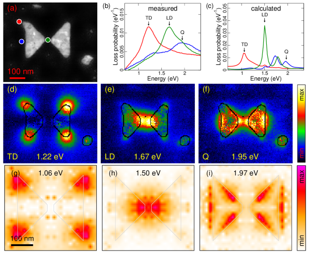
First we will discuss plasmonic properties of bowtie antennas. Typical bowtie with the wing size of nm is shown in Fig. 2(a). EEL spectra recorded at different positions reveal three distinct peaks at the energies of 1.23 eV, 1.67 eV, and 1.95 eV, as observed in Fig. 2(b). Experimental spectra are reasonably well reproduced with calculations [Fig. 2(c)]. The nature of the modes is revealed in the energy filtered maps of the loss intensity. The loss intensity is related to the plasmon electric field parallel with the trajectory of the electron beam [29], which is the largest at the charge antinodes (current nodes) of plasmon oscillations. Due to large wing angle () the lowest mode at 1.23 eV is the transverse dipole mode with the charge oscillating in the direction perpendicular to the antenna’s long axis. The mode is actually a doublet consisting of parallel and antiparallel alingment of the dipoles in both wings (bonding and antibonding transverse mode) [10]. However, due to large separation between the dipoles, the energy separation of both modes is small, considerably smaller than their spectral width. The next peak at 1.67 eV again comprises two modes, longitudinal dipole bonding and antibonding modes. The former features two loss intensity maxima at the bases of the wings, the latter features an additional maximum in the gap of the antenna. The third peak at 1.95 eV corresponds to the quadrupole mode. All these modes have been observed previously [11].
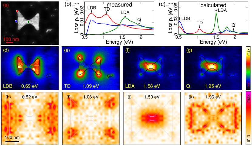
We repeat similar analysis for the diabolo antenna with nearly the same wing length nm (differences arise due to limited accuracy of the fabrication). The antenna and its spectral response are shown in Fig. 3. The presence of the conductive bridge significantly influences the longitudinal bonding mode, which exhibits a huge red shift to 0.69 eV (from 1.67 eV in the bowtie) and becomes the lowest mode. The strong impact of the bridge conductivity is related to the fact the mode exhibits a current antinode in the bridge. On the contrary, the remaining modes resolved in our EELS experiment exhibit a current node within the bridge and are therefore not very sensitive to the presence of the bridge. Their energies read for the transverse dipole mode 1.09 eV (1.23 eV in the bowtie), for the longitudinal antibonding mode 1.58 eV (1.67 eV), and for the quadrupole mode 1.95 eV (1.95 eV). Weak red shifts of diabolo modes with respect to corresponding bowtie modes can be attributed to slightly larger size of the diabolo antenna involved in the comparison.
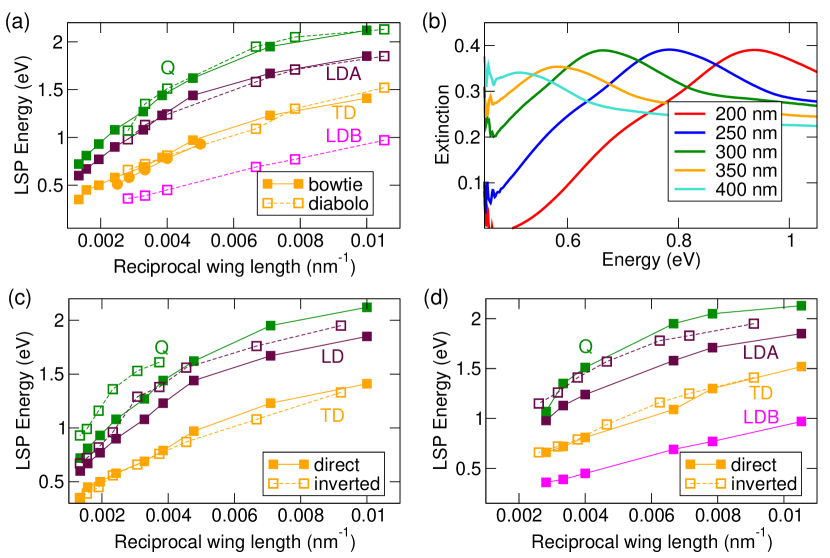
Figure 4(a) compares the energies of the modes in bowtie and diabolo antennas of different sizes. Strikingly, energies of the corresponding modes in both type of antennas are nearly identical, except for the longitudinal dipolar bonding which is pronouncedly redshifted for the diabolo antenna. There is an intuitive explanation of this observation.
The modes in the dimer plasmonic antennas (such as bowtie and diabolo) can be classified as two different types. Strongly coupled modes (such as the longitudinal bonding mode) extend to the area of the junction. Depending on the nature of the junction there is either charge transfer through the conducting bridge or capacitive charge coupling (accumulation of opposite charges at opposite sides of the insulating gap). Properties of the strongly coupled modes pronouncedly depend on the properties of the junction. As an example, the longitudinal bonding mode of the bowtie antenna exhibits an electric field hotspot at the junction while the strongly red-shifted longitudinal bonding mode of the diabolo antenna exhibits a magnetic field hotspot. Weakly coupled modes (longitudinal antibonding, transverse, and quadrupolar) avoid the area of the junction, with no charge transfer or capacitive coupling, although there still might be charge accumulation (e.g. for the longitudinal antibonding mode). The junction affects the properties of the weakly coupled modes only slightly by modifying the dielectric environment and having some impact on the spatial distribution of the near field. However, charge oscillations are not directly influenced.
We note that in addition to EELS we also performed optical transmission spectroscopy for arrays of bowtie antennas [Fig. 4(b)] which exhibit only a single resolvable spectral feature corresponding to the transverse dipolar mode. Excellent agreement between the energies of the transverse dipolar modes obtained by both methods supports our interpretation of the spectral features.
Experimental and calculated energies of plasmonic modes agree very well to each other for both the bowtie and diabolo antennas. The differences up to 0.1 eV for the lowest mode and up to 0.2 eV for the higher modes are within the experimental error.
Next, we compare direct and indirect antennas related by Babinet’s principle of complementarity. Inspection of the EEL spectra shows that complementary antennas exhibit resonances at similar energies but with different spatial distribution of the loss function (see Fig. 5). To compensate for the size differences we plot the peak energies of the EEL spectra as functions of the reciprocal wing length in Fig. 4(c,d) for bowtie and diabolo antennas, respectively. The interpolation between the experimentally retrieved points allows us to compare the energies of LSPR at identical sizes of complementary antennas. We clearly observe the validity of Babinet’s principle: corresponding LSPR have identical energy (with respect to the experimental error, which is about 0.1 eV for the lowest modes and increases for the higher modes due to their overlapping in the spectra).
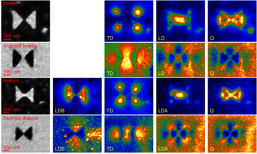
In Figure 5 we compare spatial maps of the loss function for specific LSP modes of all four antenna types. The size of the antennas is identical with respect to the fabrication uncertainty and varies between 140 nm and 150 nm (wing length). We clearly observe bowtie-diabolo duality. The modes that do not involve charge transfer through the neck of the antenna (TD, LDA, Q) have identical spatial distribution of the loss function (and therefore of the near field). They also have similar mode energies. On the other hand, the mode LDB that includes charge transfer through the bridge of diabolo antennas has significantly different energy in bowtie antennas. Due to its spectral overlap with LDA it was not possible to record its spatial map experimentally. The same duality holds for the direct as well and inverted bowtie-diabolo pairs.
Babinet complementarity is also clearly visible in Fig. 5. The corresponding modes in direct and inverted antennas, despite having identical energy, strongly differ in the spatial distribution of the near field.
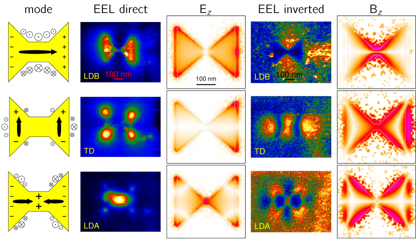
Finally, we address the question how to interpret the maps of the loss intensity and what to learn about the modes. We will first consider the case of LDB mode in the diabolo antenna. Figure 6(a) shows schematically how current oscillates and where the charge accumulates. Loss intensity recorded by EELS is proportional to the electric field projected to the trajectory of the electron [29], i.e., out of plane of the antenna. From the Gauss’s law it follows that the strongest out-of-plane field occurs just near the areas of accumulated charge. Figure 6(b,c) indeed shows maxima of experimental loss intensity and calculated out-of-plane electric field at those areas. The interpretation of the loss intensity recorded for the inverted diabolo antenna (aperture) [Fig. 6(d)] is less straightforward as there is no simple current distribution of the related plasmonic mode. Instead, we will relate the loss intensity distribution of inverted antenna to the current distribution of the direct antenna. Loss intensity in the inverted antenna is proportional to the out-of-plane electric field, which is according to Babinet’s principle proportional to the out-of-plane component of the magnetic field in the direct antenna. Indeed, magnetic field in the direct antenna according to the Ampère’s law circulates around the electric current with the maxima around the antinodes of the current [Fig. 6(a)]. Both the experimental loss intensity in the inverted antenna [Fig. 6(d)] and the calculated out-of-plane magnetic field in the direct antenna [Fig. 6(e)] exhibit maxima in the aread around the current’s antinodes.
Similar considerations can be repeated for TD mode and LDA mode or for bowtie antenna. Schemes of the charge oscillations together with the calculated electric and magnetic field distribution are shown in the second and third line of Fig. 6 for the TD and LDA mode, respectively. As in the case of LDB mode, bright spots in the loss intensity of direct antennas correspond to the strong out-of-plane component of the electric field related to the accumulated charge, and bright spots in the loss intensity of the Babinet-complementary antennas (apertures) correspond to the strong out-of-plane component of the magnetic field that circulates around antinodes of the current density.
Conclusion
We have demonstrated a unique approach of independent engineering of individual LSP modes in composite plasmonic antennas based on varying the coupling between the components from capacitive to conductive. Taking bowtie and diabolo antennas as an example, we have shown that the longitudinal dipolar mode can be significantly modified (including switching between electric and magnetic hot spot) without affecting the higher-order modes. In combination with Babinet’s principle allowing to engineer independently spectral and spatial properties of LSP modes, this represents a powerful tool for tailoring the properties of LSP modes for the phenomena and applications including Fano resonances, directional scattering, or enhanced luminescence.
Methods
Fabrication of antennas
Plasmonic antennas for EELS measurement were fabricated by focused ion beam (FIB) lithography. First, we deposited 30 nm-thick gold layer on 30 nm-thick standard TEM silicon nitride membrane with the window size of m2 (Agar Scientific). Gold layer was deposited without any adhesion layer by ion beam assisted deposition. Second, we performed FIB lithography in dual beam FIB/SEM microscope FEI Helios using gallium ions with the energy of 30 keV and ion beam current of 2.6 pA. We note that the energy (the highest available) and the current (the lowest available) are optimized for the best spatial resolution of the milling. Direct antennas were situated in the middle of a metal-free square (between m2 and m2), which is perfectly sufficient to prevent their interaction with the surrounding metallic frame [30]. Inverted antennas were fabricated as isolated antennas with the distance between two nearby structures at least of 5 m to prevent their collective interaction.
Plasmonic antennas for optical measurement were fabricated by electron beam lithography (EBL).
Electron energy loss spectroscopy
EELS measurements were performed with TEM FEI Titan equipped with GIF Quantum spectrometer operated in monochromated scanning regime at 300 kV. Beam current was set to 0.4 nA and the FWHM of the zero-loss peak was around 0.1 eV. We set convergence angle to 10 mrad, collection angle to 10.4 mrad, and dispersion of the spectrometer to 0.01 eV/pixel. We recorded EEL spectrum images with the pixel size of 5 nm, while the number of pixels depended on the antenna size. Every pixel consists of 30 cross-correlated EEL spectra with the acquisition time around 25 s for each spectrum. EEL spectra were integrated over several pixels around the positions of interest, background and zero-loss peak subtracted, and divided by the integral intensity of the whole spectrum to transform measured counts to a quantity proportional to the loss probability. EEL maps were obtained as energy-integrated intensity at the plasmon peak energy with the energy window of 0.1 eV divided pixel-by-pixel by the integral intensity of the zero-loss peak (integration window from eV to 0.5 eV).
The relation of the measured loss probability to the near field of LSP modes is as follows. The probing electron transfers a part of its energy to a LSP mode in the specimen with the probability density (so-called loss probability) reading [29]
where is the field induced by the electron moving with the velocity at the position of the electron . For the electron with the trajectory perpendicular to the sample (along the axis ) it is out-of-plane component of the field () that is relevant for the interaction. Correspondence between the loss probability and the electromagnetic local density of states projected along the electron beam trajectory has been thoroughly discussed [31, 32, 33].
Optical measurements
The far-field extinction () spectra were acquired using an infrared microscope (Bruker Hyperion 3000, 36 objective, ) coupled to a Fourier-transform infrared spectrometer (Bruker Vertex 80V). Each spectrum was referenced to a bare substrate in the vicinity of the respective antenna array.
Simulations
In all simulations, the bow-tie and diabolo antennas have been represented by two gold triangles or triangular apertures (as shown in Fig. 1) of the height of 30 nm on top of 30-nm-thick silicon nitride membrane. The adhesion layer has been neglected. The dielectric function of gold was taken from Ref. [34] and the dielectric constant of the silicon nitride membrane was set equal to 4, which is a standard approximation in the considered spectral region [35].
Electron energy loss spectra has been calculated with finite element method (FEM) using a commercial software COMSOL Multiphysics.
Data availability
The datasets analysed during the current study are available from the corresponding author on reasonable request.
References
- [1] Novotny, L. & van Hulst, N. Antennas for light. \JournalTitleNature Photonics 5, 83, DOI: 10.1038/nphoton.2010.237 (2011).
- [2] Klein, M. W., Enkrich, C., Wegener, M. & Linden, S. Second-harmonic generation from magnetic metamaterials. \JournalTitleScience 313, 502–504, DOI: 10.1126/science.1129198 (2006).
- [3] Feth, N. et al. Second-harmonic generation from complementary split-ring resonators. \JournalTitleOpt. Lett. 33, 1975–1977, DOI: 10.1364/OL.33.001975 (2008).
- [4] Atie, E. M. et al. Remote optical sensing on the nanometer scale with a bowtie aperture nano-antenna on a fiber tip of scanning near-field optical microscopy. \JournalTitleApplied Physics Letters 106, 151104, DOI: 10.1063/1.4918531 (2015).
- [5] Kinkhabwala, A. et al. Large single-molecule fluorescence enhancements produced by a bowtie nanoantenna. \JournalTitleNature Photonics 3, 654 (2009).
- [6] Yu, N. & Capasso, F. Flat optics with designer metasurfaces. \JournalTitleNature Materials 13, 139, DOI: 10.1038/nmat3839 (2014).
- [7] Nordlander, P., Oubre, C., Prodan, E., Li, K. & Stockman, M. I. Plasmon hybridization in nanoparticle dimers. \JournalTitleNano Letters 4, 899–903, DOI: 10.1021/nl049681c (2004).
- [8] Davis, T. J., Gómez, D. E. & Vernon, K. C. Simple model for the hybridization of surface plasmon resonances in metallic nanoparticles. \JournalTitleNano Letters 10, 2618–2625, DOI: 10.1021/nl101335z (2010).
- [9] Brandl, D. W., Mirin, N. A. & Nordlander, P. Plasmon modes of nanosphere trimers and quadrumers. \JournalTitleThe Journal of Physical Chemistry B 110, 12302–12310, DOI: 10.1021/jp0613485 (2006).
- [10] Koh, A. L., Fernández-Domínguez, A. I., McComb, D. W., Maier, S. A. & Yang, J. K. W. High-resolution mapping of electron-beam-excited plasmon modes in lithographically defined gold nanostructures. \JournalTitleNano Letters 11, 1323–1330, DOI: 10.1021/nl104410t (2011). PMID: 21344928.
- [11] Duan, H., Fernández-Domínguez, A. I., Bosman, M., Maier, S. A. & Yang, J. K. W. Nanoplasmonics: Classical down to the nanometer scale. \JournalTitleNano Letters 12, 1683–1689, DOI: 10.1021/nl3001309 (2012). PMID: 22313285.
- [12] Born, M., Wolf, E. & Bhatia, A. Principles of Optics: Electromagnetic Theory of Propagation, Interference and Diffraction of Light (Cambridge University Press, 1999).
- [13] Falcone, F. et al. Babinet principle applied to the design of metasurfaces and metamaterials. \JournalTitlePhys. Rev. Lett. 93, 197401, DOI: 10.1103/PhysRevLett.93.197401 (2004).
- [14] Zentgraf, T. et al. Babinet’s principle for optical frequency metamaterials and nanoantennas. \JournalTitlePhys. Rev. B 76, 033407, DOI: 10.1103/PhysRevB.76.033407 (2007).
- [15] Hentschel, M., Weiss, T., Bagheri, S. & Giessen, H. Babinet to the half: Coupling of solid and inverse plasmonic structures. \JournalTitleNano Letters 13, 4428–4433, DOI: 10.1021/nl402269h (2013).
- [16] Bitzer, A., Ortner, A., Merbold, H., Feurer, T. & Walther, M. Terahertz near-field microscopy of complementary planar metamaterials: Babinet’s principle. \JournalTitleOpt. Express 19, 2537–2545, DOI: 10.1364/OE.19.002537 (2011).
- [17] Rossouw, D. & Botton, G. A. Resonant optical excitations in complementary plasmonic nanostructures. \JournalTitleOpt. Express 20, 6968–6973, DOI: 10.1364/OE.20.006968 (2012).
- [18] Mizobata, H., Ueno, K., Misawa, H., Okamoto, H. & Imura, K. Near-field spectroscopic properties of complementary gold nanostructures: applicability of babinet’s principle in the optical region. \JournalTitleOpt. Express 25, 5279–5289, DOI: 10.1364/OE.25.005279 (2017).
- [19] von Cube, F. et al. Spatio-spectral characterization of photonic meta-atoms with electron energy-loss spectroscopy. \JournalTitleOpt. Mater. Express 1, 1009–1018, DOI: 10.1364/OME.1.001009 (2011).
- [20] Horák, M. et al. Limits of babinet’s principle for solid and hollow plasmonic antennas. \JournalTitleSci. Rep. 9, 4004, DOI: 10.1038/s41598-019-40500-1 (2019).
- [21] Chen, H.-T. et al. Complementary planar terahertz metamaterials. \JournalTitleOpt. Express 15, 1084–1095, DOI: 10.1364/OE.15.001084 (2007).
- [22] Hrtoň, M., Konečná, A., Horák, M., Šikola, T. & Křápek, V. Plasmonic antennas with electric, magnetic, and electromagnetic hot spots based on Babinet’s principle. \JournalTitlearXiv e-prints arXiv:1904.01397 (2019). 1904.01397.
- [23] Chen, Y., Chen, Y., Chu, J. & Xu, X. Bridged bowtie aperture antenna for producing an electromagnetic hot spot. \JournalTitleACS Photonics 4, 567–575, DOI: 10.1021/acsphotonics.6b00857 (2017).
- [24] Itoh, T., Yamamoto, Y. S. & Ozaki, Y. Plasmon-enhanced spectroscopy of absorption and spontaneous emissions explained using cavity quantum optics. \JournalTitleChem. Soc. Rev. 46, 3904–3921, DOI: 10.1039/C7CS00155J (2017).
- [25] Vercruysse, D. et al. Directional fluorescence emission by individual v-antennas explained by mode expansion. \JournalTitleACS Nano 8, 8232–8241, DOI: 10.1021/nn502616k (2014).
- [26] Verellen, N. et al. Fano resonances in individual coherent plasmonic nanocavities. \JournalTitleNano Letters 9, 1663–1667, DOI: 10.1021/nl9001876 (2009).
- [27] Zhang, S., Genov, D. A., Wang, Y., Liu, M. & Zhang, X. Plasmon-induced transparency in metamaterials. \JournalTitlePhys. Rev. Lett. 101, 047401, DOI: 10.1103/PhysRevLett.101.047401 (2008).
- [28] Hentschel, M., Dregely, D., Vogelgesang, R., Giessen, H. & Liu, N. Plasmonic oligomers: The role of individual particles in collective behavior. \JournalTitleACS Nano 5, 2042–2050, DOI: 10.1021/nn103172t (2011).
- [29] García de Abajo, F. J. Optical excitations in electron microscopy. \JournalTitleRev. Mod. Phys. 82, 209–275, DOI: 10.1103/RevModPhys.82.209 (2010).
- [30] Křápek, V. et al. Spatially resolved electron energy loss spectroscopy of crescent-shaped plasmonic antennas. \JournalTitleOpt. Express 23, 11855–11867, DOI: 10.1364/OE.23.011855 (2015).
- [31] García de Abajo, F. J. & Kociak, M. Probing the photonic local density of states with electron energy loss spectroscopy. \JournalTitlePhys. Rev. Lett. 100, 106804, DOI: 10.1103/PhysRevLett.100.106804 (2008).
- [32] Kociak, M. & Stéphan, O. Mapping plasmons at the nanometer scale in an electron microscope. \JournalTitleChem. Soc. Rev. 43, 3865–3883, DOI: 10.1039/C3CS60478K (2014).
- [33] Hohenester, U., Ditlbacher, H. & Krenn, J. R. Electron-energy-loss spectra of plasmonic nanoparticles. \JournalTitlePhys. Rev. Lett. 103, 106801, DOI: 10.1103/PhysRevLett.103.106801 (2009).
- [34] Johnson, P. B. & Christy, R. W. Optical constants of the noble metals. \JournalTitlePhys. Rev. B 6, 4370–4379, DOI: 10.1103/PhysRevB.6.4370 (1972).
- [35] Schmidt, F. P., Ditlbacher, H., Hofer, F., Krenn, J. R. & Hohenester, U. Morphing a plasmonic nanodisk into a nanotriangle. \JournalTitleNano Letters 14, 4810–4815, DOI: 10.1021/nl502027r (2014).
Acknowledgement
We acknowledge the support by the Czech Science Foundation (grant No. 17-25799S), Ministry of Education, Youth and Sports of the Czech Republic (projects CEITEC 2020, No. LQ1601, and CEITEC Nano RI, No. LM2015041), and Brno University of Technology (grant No. FSI/STI-J-18-5225).
Author information
Contributions
V.K. conceived and coordinated research with help of T.S. Mi.H. and J.B fabricated the antennas, Mi.H. performed their electron spectrocopy with the assistence of M.S., F.L. performed optical spectroscopy, Ma.H. and A.K. performed numerical simulations. All authors were involved in the data processing and interpretation. V.K. and Mi.H. wrote the manuscript.
Competing interests
The authors declare no competing interests.